 | –≠–ª–µ–∫—Ç—Ä–æ–Ω–Ω—ã–π –∫–æ–º–ø–æ–Ω–µ–Ω—Ç: MC141556 | –°–∫–∞—á–∞—Ç—å:  PDF PDF  ZIP ZIP |
MOTOROLA
SEMICONDUCTOR TECHICAL DATA
REV 3.0
03/98
© Motorola, Inc. 1998
Order this document
by MC141556
Product Preview
USB Hub Controller
CMOS
This device is a self-contained USB Hub which complies with USB Hub spec
Rev 1.0. This device is used to expand the USB ports of your PC system while
needed. Because of its self-contained and bus-powered/self-powered capabil-
ity, it can hide the complexity from the user and be flexibly placed anywhere,
such as monitor, keyboard, motherboard, hub-box, etc. The MC141556 con-
sists of Serial Interface Engine(SIE), Hub Repeater, and Hub Controller, sup-
porting one upstream port and up to five downstream ports. It also provides
optional IIC(M_BUS) programmable Vendor ID and Product ID.
Both Low speed mode (1.5 Mbps) and Full speed mode (12 Mbps) are sup-
ported by automatically detecting which data line (D+ or D-) is pulled high
whenever downstream devices are connected to the bus or at power-up.
MC141556 can be self-powered or bus-powered. When self-powered,
MC141556 is powered by external 5 volt supply and capable of delivering
500mA current to each downstream port. Power management for all down-
stream ports supports power-switching and overcurrent detection with Individ-
ual or Ganged control; a self-powered MC141556 supports Individual control
only, but bus-powered MC141556 supports either Individual or Ganged control.
When Ganged control, PWRSW1 and OVR1 are dedicated for power manage-
ment.
IIC(M_BUS) interface is provided to set up customized Vendor ID, Product
ID, Power Mode, Power Management Mode, Number of Downstream Ports
and Overcurrent Debounce Setting.
Features Highlight
Hub
∑ Self-contained Hub Includes Serial Interface Engine (SIE), Hub Repeater
and Hub Controller
∑ Universal Serial Bus (USB) Hub Version 1.0 Compliant
∑ One Upstream Port and Up To Five Downstream Ports
∑ Self-powered or Bus-powered
∑ Individual/Ganged Downstream Port Power Switching
∑ Individual/Ganged Downstream Port Overcurrent Detection
∑ All Downstream Ports Support Full Speed and Low Speed Operation
∑ Suspend and Resume Operations
∑ Host Reset Operation
∑ IIC (M_BUS) interface
General Characteristics
∑ 28 DIP Package
∑ Crystal Input 24MHz
∑ Internal 3.3Volt Regulator
∑ Single 5Volt Power Supply
∑ Low-power CMOS Technology
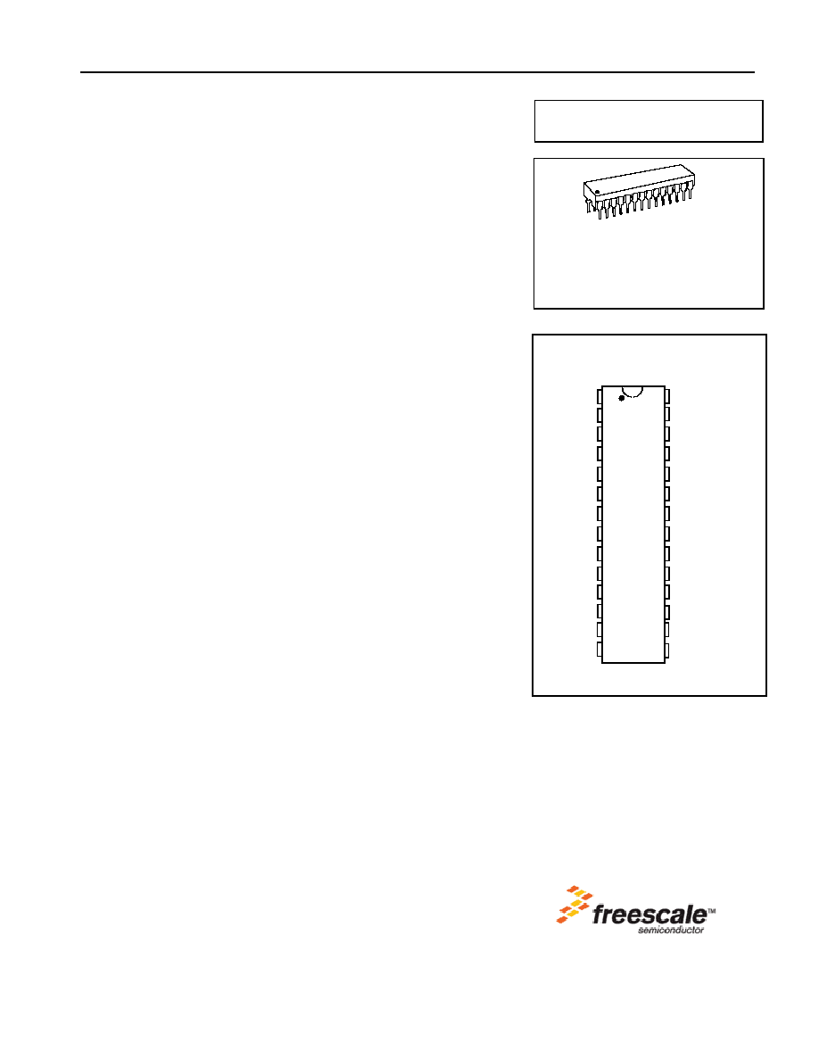
MC141556
P SUFFIX
PLASTIC PACKAGE
CASE 655
ORDERING INFORMATION
MC141556P
Plastic Dip
28 1
VDD
OSC1
OSC2
IICEN
OVR1
VDD3CAP
PWRSW4
DM4
PWRSW3
DM3
PWRSW1
DM2
VSS
OVR2
OVR3
OVR4
PWRSW2
DP2
DM1
DP3
DP4
DM0
DP0
DP1
2
3
4
5
6
7
8
9
10
11
25
26
17
18
19
20
21
22
23
24
1
12
27
28
13
15
16
14
PWRSW5/SDA
DP5/SEL1
DM5/SEL0
OVR5/GANG/SCL
PIN ASSIGNMENT
This document contains information on a new product. Specifications and information herein are subject to change without notice.
F
r
e
e
s
c
a
l
e
S
e
m
i
c
o
n
d
u
c
t
o
r
,
I
Freescale Semiconductor, Inc.
For More Information On This Product,
Go to: www.freescale.com
n
c
.
.
.
RoHS-compliant and/or Pb- free versions of Freescale products have the functionality
and electrical characteristics of their non-RoHS-compliant and/or non-Pb- free
counterparts. For further information, see http://www.freescale.com or contact your
Freescale sales representative.
For information on Freescale.s Environmental Products program, go to
http://www.freescale.com/epp.
MC141556
2
MOTOROLA
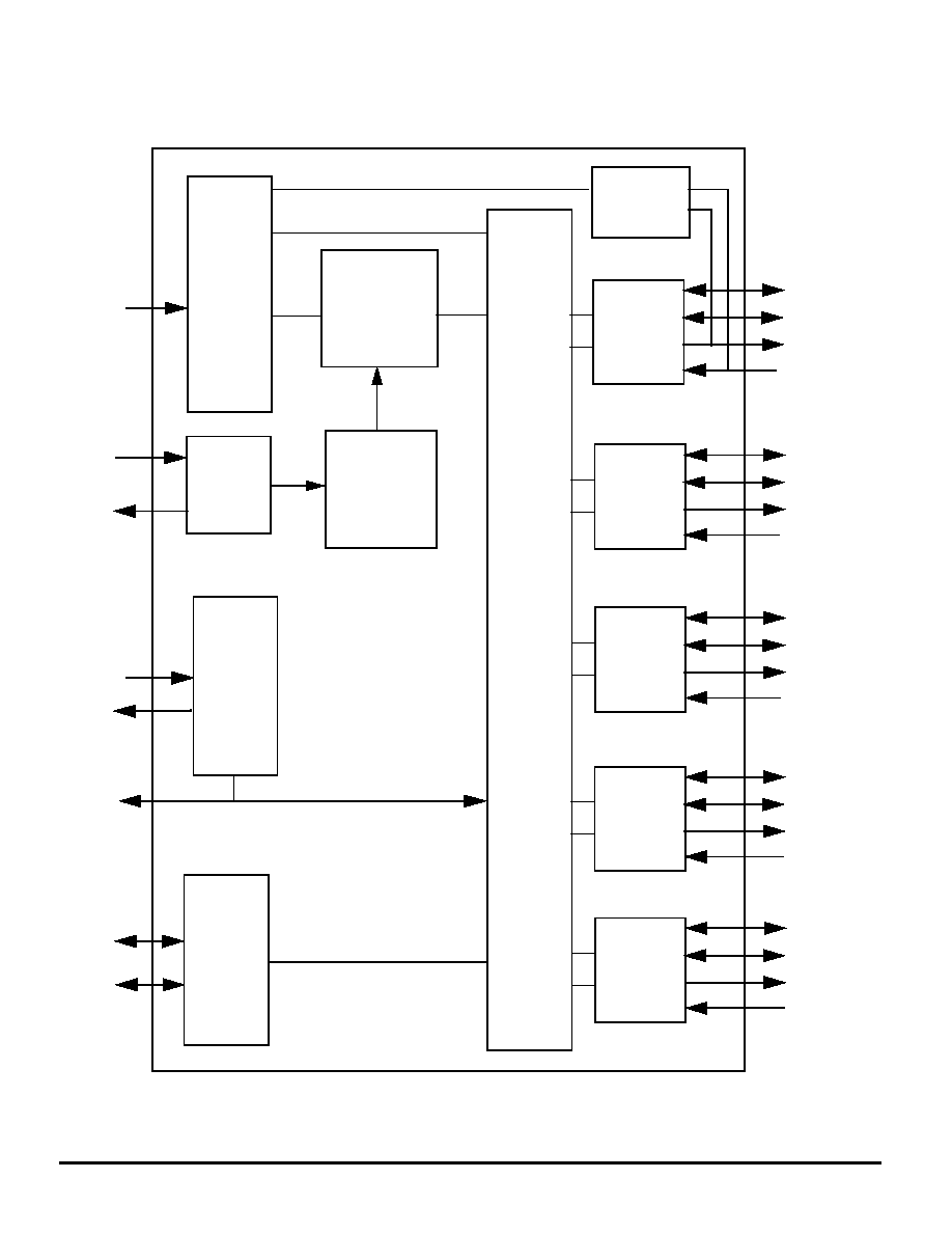
Figure1. BLOCK DIAGRAM
Root
VSS
DP0
DM0
OSC2
OSC1
VDD
2
4
6
7
1
VDD3CAP
Hub
(SIE)
IICEN
5
8
3
Controller
Port
Clock
Doubler
Power
Supply
&
3.3V
Regulator
3.3 Volts
Serial Interface
Engine
Frame Counter
(1ms)
48MHz
DM5/SEL0
DP5/SEL1
25
27
28
OVR5/GANG/SCL
PWRSW5/SDA
26
Repeater
PORT 5
Downstream
IIC Module
DM4
DP4
21
23
24
OVR4
PWRSW4
22
PORT 4
Downstream
DM3
DP3
17
19
20
OVR3
PWRSW3
18
PORT 3
Downstream
DM2
DP2
13
15
16
OVR2
PWRSW2
14
PORT 2
Downstream
DM1
DP1
9
11
12
OVR1
PWRSW1
10
PORT 1
Downstream
F
r
e
e
s
c
a
l
e
S
e
m
i
c
o
n
d
u
c
t
o
r
,
I
Freescale Semiconductor, Inc.
For More Information On This Product,
Go to: www.freescale.com
n
c
.
.
.

MC141556
3
MOTOROLA
ABSOLUTE MAXIMUM RATINGS
Voltage Referenced to VSS
NOTE: Maximum Ratings are those values beyond which damage to the device may occur.
Functional operation should be restricted to the limits in the Electrical Characteristics
tables or Pin Description section.
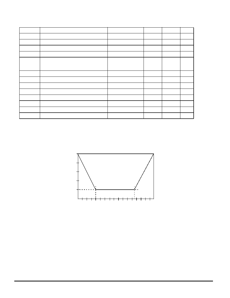
AC ELECTRICAL CHARACTERISTICS
(VDD/VDD(A) = 5.0 V, VSS/VSS(A) = 0 V, TA = 25C,
Voltage Referenced to VSS)
FULL SPEED MODE CHARACTERISTICS
LOW SPEED MODE CHARACTERISTICS
Symbol
Characteristic
Value
Unit
VDD
Supply Voltage
- 0.3 to + 7.0
V
Vin
Input Voltage
VSS ≠ 0.3 to
VDD + 0.3
V
Id
Current Drain per Pin Excluding VDD and VSS
25
mA
Ta
Operating Temperature Range
0 to 85
∞
C
Tstg
Storage Temperature Range
≠ 65 to + 150
∞
C
Symbol
Parameter
Conditions
Min
Max
Unit
tr
tf
Rise Time for DP/DM
Fall Time for DP/DM
Cload = 50 pF
Cload = 50 pF
4
4
20
20
ns
ns
tRFM
Rise/Fall Time Matching
(tr/tf) x 100
90
110
%
VCRS
Output Signal Crossover Voltage
--
1.3
2.0
V
Symbol
Parameter
Conditions
Min
Max
Unit
tr
tf
Rise Time for DP/DM
Fall Time for DP/DM
Cload = 50 pF to 350 pF
Cload = 50 pF to 350 pF
75
75
300
300
ns
ns
tRFM
Rise/Fall Time Matching
(tr/tf) x 100
80
120
%
VCRS
Output Signal Crossover Voltage
--
1.3
2.0
V
This device contains protection circuitry to guard
against damage due to high static voltages or
electric fields. However, precautions must be
taken to avoid applications of any voltage higher
than maximum rated voltages to this high-imped-
ance circuit. For proper operation, Vin and Vout
should be constrained to the range VSS
(Vin
or Vout)
VDD.
Unused inputs must always be tied to an appro-
priate logic voltage level (e.g., either VSS or
VDD). Unused outputs must be left open.
90%
10%
tr
DP
DM
V
OL
V
OH
VCRS
90%
10%
tf
DM
Cload
Cload
R1
R1
R2
R2
R3
Data
R1 = 22
R2 = 15
R3 = 1.5
Figure 2. Differential Driver Switching Load
Figure 3. Differential Driver Switching Characteristics
k
k
F
r
e
e
s
c
a
l
e
S
e
m
i
c
o
n
d
u
c
t
o
r
,
I
Freescale Semiconductor, Inc.
For More Information On This Product,
Go to: www.freescale.com
n
c
.
.
.
MC141556
4
MOTOROLA
DC CHARACTERISTICS
VDD/VDD(A) = 5.0 V
±
10%, VSS/VSS(A) = 0 V, TA = 25
∞
C, Voltage Referenced to VSS
Symbol
Parameter
Conditions
Min
Max
Unit
VBUS
Powered (Host or Hub) Port
--
4.65
5.25
V
VBUS
Bus-powered Hub Port
--
4.40
5.25
V
VOH
High Level Output Voltage
--
2.8
3.6
V
VOL
Low Level Output Voltage
--
--
0.3
V
VIL
VIH
Digital Input Voltage
Logic Low
Logic High
--
--
0.7 VDD
0.3 VDD
--
V
V
III
High-Z Leakage Current (output pins)
--
≠ 10
+ 10
µ
A
III
Input Current
--
≠ 10
+ 10
µ
A
IDD
Supply Current (No Load on Any Output)
--
--
+ 25
mA
ICCINIT
Unconfig. Function/Hub (in)
--
--
100
mA
VDI
Differential Input Sensitivity
|(D+)-(D-)| Refer to Figure 4
0.2
--
V
VCM
Differential Common Mode Range
Includes VDI range
0.8
2.5
V
VSE
Single Ended Receiver Threshold
--
0.8
2.0
V
CHPB
Downstream Hub Port Bypass Capacitance
Vbus to GND
120
--
µ
F
0.0
0.2 0.4 0.6 0.8 1.0 1.2 1.4 1.6 1.8 2.0 2.2 2.4 2.6 2.8 3.0 3.2
0.2
0.4
0.6
0.8
1.0
Common Mode Input Voltage (volts)
M
i
n
i
m
u
m
D
i
f
f
e
r
e
n
t
i
a
l
S
e
n
s
i
t
i
v
i
t
y
(
v
o
l
t
s
)
Figure 4. Differential Input Sensitivity Over Entire Common Mode Range
F
r
e
e
s
c
a
l
e
S
e
m
i
c
o
n
d
u
c
t
o
r
,
I
Freescale Semiconductor, Inc.
For More Information On This Product,
Go to: www.freescale.com
n
c
.
.
.
MC141556
5
MOTOROLA
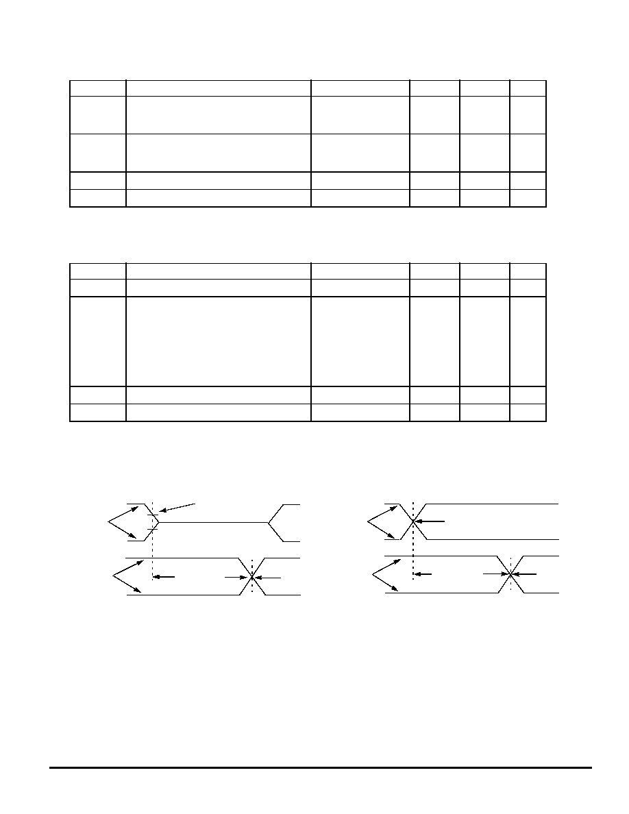
LOW SPEED OPERATING HUB ELECTRICAL CHARACTERISTICS
Symbol
Parameter
Conditions
Min
Max
Unit
tLHDD
Hub Differential Data Delay
Figure 5, Figure 6
--
300
ns
tLDHJ1
tLDHJ2
tLDHJ2
tLDHJ2
Hub Differential Driver Jitter (including cable)
Downstream:
To Next Transition
For Paired Transitions
Upstream:
To Next Transition
For Paired Transitions
--
-45
-15
-45
-45
45
15
45
45
ns
ns
ns
ns
tSOP
Data Bit Width Distortion After SOP
--
-60
45
ns
tLHESK
Hub EOP Output Width Skew
--
-300
300
ns
FULL SPEED OPERATING HUB ELECTRICAL CHARACTERISTICS
Symbol
Parameter
Conditions
Min
Max
Unit
tHDD1
tHDD2
Hub Differential Data Delay
(with cable)
(without cable)
Figure 5, Figure 6
--
--
70
40
ns
ns
tHDJ1
tHDJ2
Hub Differential Driver Jitter (including cable)
To Next Transition
For Paired Transitions
--
-3
-1
3
1
ns
ns
tSOP
Data Bit Width Distortion After SOP
--
-5
3
ns
tHESK
Hub EOP Output Width Skew
--
-15
15
ns
50% Point of
Initial Swing
Upstream
End of
Cable
Vss
Vss
Downstream
Port
Hub Delay
Downstream
t
HDD1
Crossover
Point
Vss
Hub Delay
Downstream
t
HDD1
, t
HDD2
Crossover
Point
Upstream
End of
Cable
Vss
Downstream
Port
Crossover
Point
Figure 5. Downstream Hub Delay
Figure 6. Upstream Hub Delay
F
r
e
e
s
c
a
l
e
S
e
m
i
c
o
n
d
u
c
t
o
r
,
I
Freescale Semiconductor, Inc.
For More Information On This Product,
Go to: www.freescale.com
n
c
.
.
.