 | –≠–ª–µ–∫—Ç—Ä–æ–Ω–Ω—ã–π –∫–æ–º–ø–æ–Ω–µ–Ω—Ç: MC14467P | –°–∫–∞—á–∞—Ç—å:  PDF PDF  ZIP ZIP |
MC14467-1
Rev 4, 05/2005
Freescale Semiconductor
Technical Data
© Freescale Semiconductor, Inc., 2005. All rights reserved.
Low-Power CMOS
Ionization Smoke Detector IC
The MC14467-1, when used with an ionization chamber and a small number
of external components, will detect smoke. When smoke is sensed, an alarm is
sounded via an external piezoelectric transducer and internal drivers. This circuit
is designed to operate in smoke detector systems that comply with UL217 and
UL268 specifications.
Features
∑
Ionization Type with On-Chip FET Input Comparator
∑
Piezoelectric Horn Driver
∑
Guard Outputs on Both Sides of Detect Input
∑
Input-Production Diodes on the Detect Input
∑
Low-Battery Trip Point, Internally Set, can be Altered Via External Resistor
∑
Detect Threshold, Internally Set, can be Altered Via External Resistor
∑
Pulse Testing for Low Battery Uses LED for Battery Loading
∑
Comparator Outputs for Detect and Low Battery
∑
Internal Reverse Battery Protection
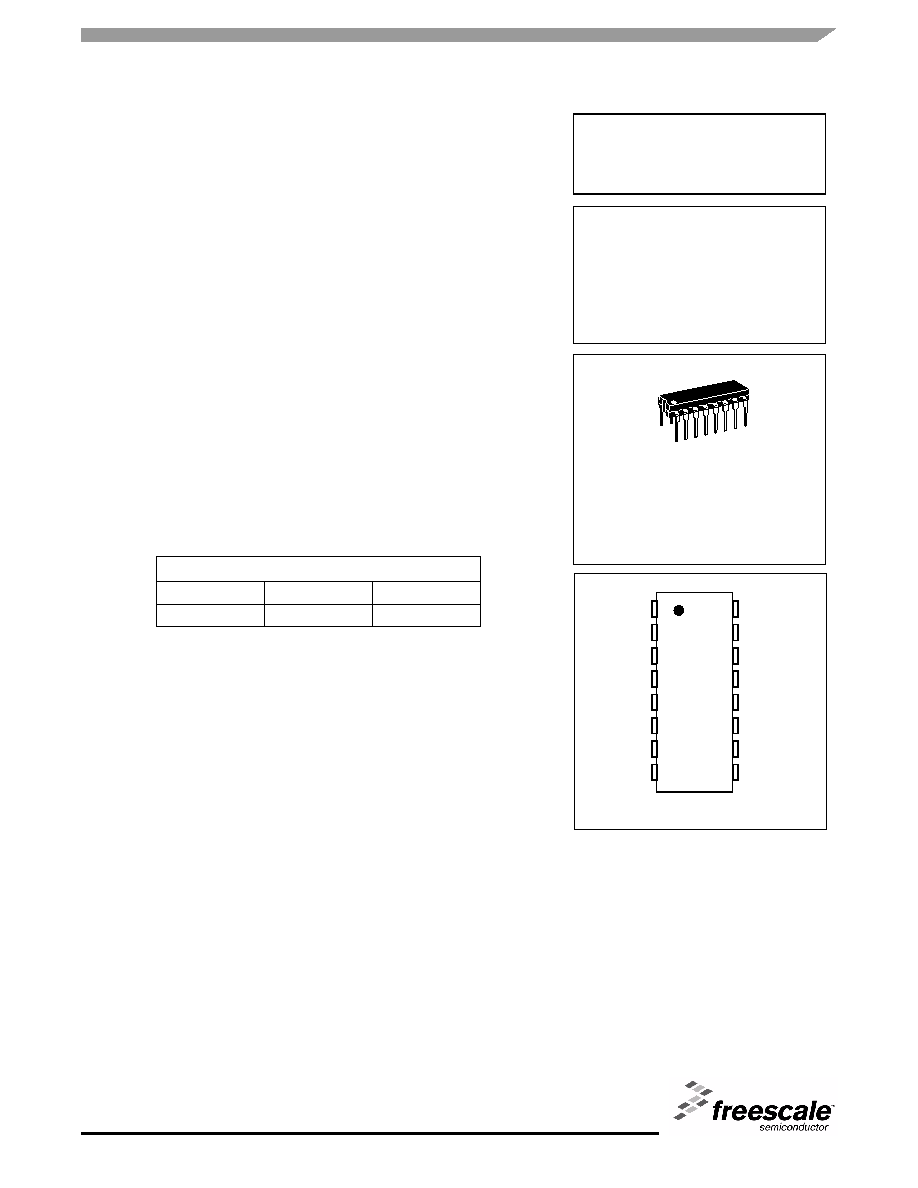
ORDERING INFORMATION
Device
Case No.
Package
MC14467P1
648-08
Plastic Dip
MC14467-1
LOW-POWER CMOS
IONIZATION
SMOKE DETECTOR IC
P SUFFIX
16-LEAD PLASTIC DIP
CASE 648-08
16
15
14
13
12
11
10
9
1
2
3
4
5
6
7
8
N/C
LED
V
DD
Guard Lo-z
Silver
Brass
V
SS
Detect
Comp. OUT
Low V Set
Low V
Comp. OUT
Timing
Resistor
Feedback
Osc Capacitor
Sensitivity Set
Detect Input
Guard Hi-z
Figure 1. Pin Connections

Sensors
2
Freescale Semiconductor
MC14467-1
Figure 2. Block Diagram
Table 1. Maximum Ratings
(1)
(Voltages referenced to V
SS
)
1. Maximum Ratings are those values beyond which damage to the device may occur. This device contains circuitry to protect the inputs
against damage due to high static voltages or electric fields; however, it is advised that normal precautions be taken to avoid application of
any voltage higher than maximum rated voltages to this high impedance circuit. For proper operation it is recommended that except for pin 8,
V
in
and V
out
be constrained to the range V
SS
(V
in
or V
out
) V
DD
. For pin 8, refer to the Electrical Characteristics.
Rating
Symbol
Value
Unit
DC Supply Voltage
V
DD
-0.5 to + 15
V
Input Voltage, All Inputs Except Pin 8
V
in
-0.25 to V
DD
+ 0.25
V
DC Current Drain per Input Pin, Except Pin 15 = 1 mA
I
10
mA
DC Current Drain per Output Pin
I
30
mA
Operating Temperature Range
T
A
-10 to +60
∞C
Storage Temperature Range
T
stg
-55 to + 125
∞C
Reverse Battery Time
t
RB
5.0
s
+
≠
+
≠
+
≠
V
DD
Led Driver
5
6
9
10
11
8
Priezoelectric
Horn Driver
4
V
DD
V
DD
V
DD
Low Battery Comp.
Latch
80 K
V
DD
3
7
12
Oscillator
Timer
1045 K
13
1125 K
15
Detect Input
14
Lo-Z
Active
Guard
1
Latch

Sensors
Freescale Semiconductor
3
MC14467-1
Table 2. Recommended Operating Conditions
(Voltages referenced to V
SS
)
Parameter
Symbol
Value
Unit
Supply Voltage
V
DD
9.0
V
Timing Capacitor
--
0.1
µF
Timing Resistor
--
8.2
M
Battery Load (Resistor or LED)
--
10
mA
Table 3. Electrical Characteristics
(Voltages referenced to V
SS
, T
A
= 25
∞
C)
Characteristic
Symbol
V
DD
V
DC
Min
Typ
(1)
1. Data labelled "Typ'' is not to be used for design purposes but is intended as an indication of the IC's potential performance.
Max
Unit
Operating Voltage
V
DD
--
6.0
--
12
V
Output Voltage
Piezoelectric Horn Drivers (I
OH
= -16 mA)
Comparators (I
OH
= -30
µA)
Piezoelectric Horn Drivers (I
OL
= +16 mA)
Comparators (I
OL
= +30
µA)
V
OH
V
OL
7.2
9.0
7.2
9.0
6.3
8.5
--
--
--
8.8
--
0.1
--
--
0.9
0.5
V
V
Output Voltage - LED Driver, I
OL
= 10 mA
V
OL
7.2
--
--
3.0
V
Output Impedance, Active Guard
Pin 14
Pin 16
Lo-Z
Hi-Z
9.0
9.0
--
--
--
--
10
1000
k
Operating Current (R
bias
= 8.2 M
)
I
DD
9.0
12.0
--
--
5.0
--
9.0
12.0
µA
Input Current - Detect (40% R.H.)
I
in
9.0
--
--
±1.0
pA
Internal Set Voltage
Low Battery
Sensitivity
V
low
V
set
9.0
--
7.2
47
--
50
7.8
53
V
%V
DD
Hysteresis
v
hys
9.0
75
100
150
mV
Offset Voltage (measured at Vin = VDD/2
Active Guard
Detect Comparator
V
OS
9.0
9.0
--
--
--
--
±100
±50
mV
Input Voltage Range, Pin 8
V
in
--
VSS - 10
--
VDD + 10
V
Input Capacitance
C
in
--
--
5.0
--
pF
Common Mode Voltage Range, Pin 15
V
cm
--
0.6
--
VDD - 2
V

Sensors
4
Freescale Semiconductor
MC14467-1
Figure 3. Typical LED Output I-V Characteristic
Figure 4. Typical Comparator Output I-V Characteristic
Figure 5. Typical P Horn Driver Output I-V Characteristic
Table 4. Timing Parameters
(C = 0.1
µ
F, R
bias
= 8.2 M
, V
DD
= 9.0 V, T
A
= 25
∞
C, See
Figure 7
)
Characteristics
Symbol
Min
Typ
(1)
Max
Units
Oscillator Period
No Smoke
Smoke
t
CI
1.34
32
1.67
40
2.0
48
s
ms
Oscillator Rise Time
t
r
8.0
10
12
ms
Horn Output
On Time
(During Smoke)
Off Time
PW
on
PW
off
120
60
160
80
208
104
ms
ms
LED Output
Between Pulses
On Time
t
LED
PW
on
32
8.0
40
10
48
12
s
ms
Horn Output
On Time
(During Low Battery)
Between Pulses
t
on
t
off
8.0
32
10
40
12
48
ms
s
1. Data labelled "Typ" is not to be used for design purposes but is intended as an indication of the IC's potential performance.
V
DS
, Drain To Source Voltage (V
DC
)
0
1
2
3
4
5
6
7
8
9
10
0.1
1.0
10.0
100.0
V
DD
= 9.0 V
DC
I
D
, D
r
ain C
u
rre
nt (m
A)
V
DD
= 7.2 V
DC
T
A
= 25∞C
V
DS
, Drain To Source Voltage (V
DC)
0
1
2
3
4
5
6
7
8
9
10
0.01
0.1
1.0
10.0
V
DD
= 9.0 V
DC
or 7.2 V
DC
T
A
= 25∞C
P-CH Source
And N-CH
Sink Current
I
D
,
Dr
ai
n Cu
rr
en
t
(m
A)
0
1
2
3
4
5
6
7
8
9
1.0
10.0
100.0
1000.0
I
D
, Drain
Curr
ent
(mA)
0
1
2
3
4
5
6
7
8
9
10
1.0
10.0
100.0
1000.0
V
DS
, Drain To Source Voltage (V
DC
)
10
V
DS
, Drain To Source Voltage (V
DC
)
I
D
,
Drain
Curr
ent
(mA)
V
DD
= 9.0 V
DC
V
DD
= 7.2 V
DC
TA = 25∞C
P-CH Source Current
V
DD
= 9.0 V
DC
T
A
= 25∞C
N-CH Sink Current
V
DD
= 7.2 V
DC
Sensors
Freescale Semiconductor
5
MC14467-1
DEVICE OPERATION
Timing
The internal oscillator of the MC14467-1 operates with a
period of 1.67 seconds during no-smoke conditions. Each
1.67 seconds, internal power is applied to the entire IC and a
check is made for smoke, except during LED pulse, Low
Battery Alarm Chirp, or Horn Modulation (in smoke). Every 24
clock cycles a check is made for low battery by comparing
V
DD
to an internal zener voltage. Since very small currents
are used in the oscillator, the oscillator capacitor should be of
a low leakage type.
Detect Circuitry
If smoke is detected, the oscillator period becomes 40 ms
and the piezoelectric horn oscillator circuit is enabled. The
horn output is modulated 160 ms on, 80 ms off. During the off
time, smoke is again checked and will inhibit further horn
output if no smoke is sensed. During smoke conditions the
low battery alarm is inhibited, but the LED pulses at a 1.0 Hz
rate.
An active guard is provided on both pins adjacent to the
detect input. The voltage at these pins will be within 100 mV
of the input signal. This will keep surface leakage currents to
a minimum and provide a method of measuring the input
voltage without loading the ionization chamber. The active
guard op amp is not power strobed and thus gives constant
protection from surface leakage currents. Pin 15 (the Detect
input) has internal diode protection against static damage.
Sensitivity/Low Battery Thresholds
Both the sensitivity threshold and the low battery voltage
levels are set internally by a common voltage divider (please
see
Figure 2
) connected between V
DD
and V
SS
. These
voltages can be altered by external resistors connected from
pins 3 or 13 to either V
DD
or V
SS
. There will be a slight
interaction here due to the common voltage divider network.
The sensitivity threshold can also be set by adjusting the
smoke chamber ionization source.
Test Mode
Since the internal op amps and comparators are power
strobed, adjustments for sensitivity or low battery level could
be difficult and/or time-consuming. By forcing Pin 12 to V
SS
,
the power strobing is bypassed and the outputs, Pins 1 and
4, constantly show smoke/no smoke and good battery/low
battery, respectively. Pin 1 = V
DD
for smoke and Pin 4 = V
DD
for low battery. In this mode and during the 10 ms power
strobe, chip current rises to approximately 50
µA.
LED Pulse
The 9-volt battery level is checked every 40 seconds
during the LED pulse. The battery is loaded via a 10 mA
pulse for 10 ms. If the LED is not used, it should be replaced
with an equivalent resistor such that the battery loading
remains at 10 mA.
Hysteresis
When smoke is detected, the resistor/divider network that
sets sensitivity is altered to increase sensitivity. This yields
approximately 100 mV of hysteresis and reduces false
triggering.
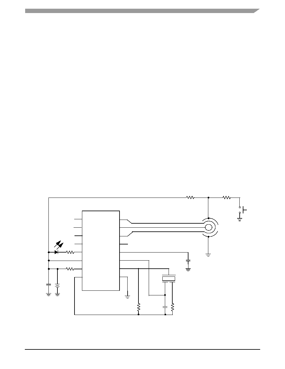
Figure 6. Typical Application as Ionization Smoke Detector
MC14467-1
1
16
2
3
4
5
6
7
8
15
14
13
12
11
10
9
Test
+
9.0 V
8.2 M
330
1.5 M
*
220 k
*
0.1 µF
1M
1M
0.1 µF
0.001* µF
*NOTE: Component values may change depending on type of piezoelectric horn used.