 | –≠–ª–µ–∫—Ç—Ä–æ–Ω–Ω—ã–π –∫–æ–º–ø–æ–Ω–µ–Ω—Ç: MC33397DW | –°–∫–∞—á–∞—Ç—å:  PDF PDF  ZIP ZIP |

MOTOROLA
SEMICONDUCTOR TECHNICAL DATA
This document contains certain information on a new product.
Specifications and information herein are subject to change without notice.
© Motorola, Inc. 2003
33397 Simplified Application Diagram
Document order number: MC33397/D
Rev 2.0, 03/2003
33397
Advance Information
DUAL/HEX LOW-SIDE SWITCH
Dual/Hex Low-Side Switch with
Both SPI and Parallel Input Control
The 33397 is a low-side switch that is user configurable to be either two
333 m
outputs (dual mode) or six 900 m outputs (hex mode). Each output
is internally current limited and short-circuit protected. Output fault detection
capability includes "off state" open loads and "on state" short-to-battery
conditions. Faults for each output are latched into the fault register and serially
shifted out during serial communication.
Features
∑ User Configurable to be Either Two 333 m
Outputs (Dual Mode) or Six
900 m
Outputs (Hex Mode)
∑ Output Inductive Energy Clamps
∑ Parallel Input (3.3 V and 5.0 V Compatible) or Serial Peripheral Interface
(SPI) Control
∑ 8-Bit SPI Control and Fault Diagnostics
∑ Short-to-Battery Detection and Shutdown with Automatic Retry
∑ OFF-State Open-Circuit Detection
∑ Programmable Overvoltage Shutdown (V
PWR
Pin)
∑ Undervoltage Shutdown (V
DD
Pin)
∑ Sleep Mode--I
DD
25 µA (1.0 µA Typical)
DW SUFFIX
PLASTIC PACKAGE
CASE 751E
24-LEAD SOICW
ORDERING INFORMATION
Device
Temperature
Range (T
A
)
Package
MC33397DW/R2
-40 to 125∞C
24 SOICW
Micro-
controller
with Bus
CMOS
Input
Logic
CMOS
Serial
Shift
Registers
and
Latches
Output
Switches
and
Sense
Circuits
+V
BAT
5-8, 17-20
GND
1
2
11
12
14
23
A5
A4
A3
A2
A1
A0
V
PWR
24
V
DD
13
EN
EN
CS
SCLK
SI
SO
15
10
3
4
9
33397
F
r
e
e
s
c
a
l
e
S
e
m
i
c
o
n
d
u
c
t
o
r
,
I
Freescale Semiconductor, Inc.
For More Information On This Product,
Go to: www.freescale.com
n
c
.
.
.
33397
MOTOROLA ANALOG INTEGRATED CIRCUIT DEVICE DATA
2
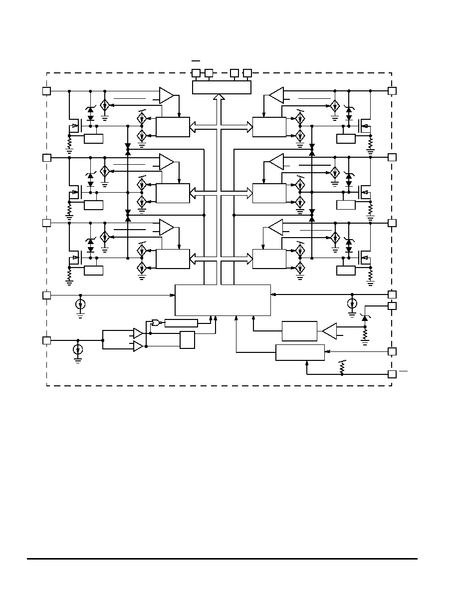
Figure 1. 33397 Simplified Block Diagram
+
-
+
-
+
-
-
+
-
+
-
+
-
+
-
+
+
-
8-Bit SPI Interface
Logic
Logic
Logic
Logic
Logic
Logic
Parallel Gate Control
and
Mode Control Logic
I
LIMIT
I
LIMIT
I
LIMIT
I
LIMIT
10
µ
s Filter
Overvoltage
Shutdown
Low V
DD
Detect
and POR Timer
S
R
Q
0.75 V
DD
0.25 V
DD
V
PWR
1.2
1.2
50 V
50 V
50 V
50 V
50 V
50 V
40
µ
A
40
µ
A
40
µ
A
40
µ
A
40
µ
A
40
µ
A
3.0 V
3.0 V
3.0 V
3.0 V
3.0 V
3.0 V
Sleep Mode
Sleep Mode
Sleep Mode
Sleep Mode
Sleep Mode
Sleep Mode
Dual Mode
Dual Mode
Dual Mode
Dual Mode
CS
SI
SO SCLK
10
µ
A
10
µ
A
10
µ
A
30 V
3.0 V
V
DD
1.2
1.2
1.2
1.2
V
DD
P1
EN
A3
A2
A1
I
LIMIT
I
LIMIT
P2
P0
A5
A4
A0
F
r
e
e
s
c
a
l
e
S
e
m
i
c
o
n
d
u
c
t
o
r
,
I
Freescale Semiconductor, Inc.
For More Information On This Product,
Go to: www.freescale.com
n
c
.
.
.

MOTOROLA ANALOG INTEGRATED CIRCUIT DEVICE DATA
33397
3
PIN FUNCTION DESCRIPTION
Pin
Pin Name
Description
1, 2, 11, 12,
14, 23
A0≠A5
Power outputs
3
SCLK
SPI clock input
4
SI
SPI serial input
5≠8, 17≠20
GND
Power and signal ground
9
SO
SPI serial output
10
CS
SPI chip select
13
V
DD
Supply input pin
15
EN
Enable
16
P0
In hex mode, P0 controls output A0. In dual mode, P0 controls outputs A0, A4, and A5 simultaneously
21
P1
In hex mode, P1 controls output A1. In dual mode, P2 controls outputs A1, A2, and A3 simultaneously
22
P2
In hex mode, P2 controls output A2. P2 is also the mode control pin. If 0.25*V
DD
<P2<0.75*V
DD
for more than
10 µs, the 33397 will change to dual mode
24
V
PWR
Overvoltage threshold shutdown monitoring pin (not a power supply pin for the IC)
V
PWR
GND
GND
GND
GND
P0
EN
A1
V
DD
A0
P2
P1
A5
GND
GND
GND
GND
SO
CS
A2
A4
SCLK
SI
A3
5
6
7
8
9
10
11
12
2
3
4
24
20
19
18
17
16
15
13
23
22
21
14
1
F
r
e
e
s
c
a
l
e
S
e
m
i
c
o
n
d
u
c
t
o
r
,
I
Freescale Semiconductor, Inc.
For More Information On This Product,
Go to: www.freescale.com
n
c
.
.
.

33397
MOTOROLA ANALOG INTEGRATED CIRCUIT DEVICE DATA
4
MAXIMUM RATINGS
All voltages are with respect to ground unless otherwise noted.
Rating
Symbol
Value
Unit
Power Supply Voltage
V
PWR
50
V
Logic Supply Voltage
V
DD
-0.3 to 7.0
V
Input Pin Voltage
V
IN
-0.3 to V
DD
+0.3
V
ESD Voltage
Human Body Model (Note 1)
Machine Model (Note 2)
V
ESD1
V
ESD2
±2000
±200
V
Single Pulse Output Clamp Energy
I
O
=500 mA, T
J
=150
∞C (Hex Mode)
I
O
=1.5 A, T
J
=150
∞C (Dual Mode)
J
CLAMP1
J
CLAMP1
50
100
mJ
Recommended SPI Operating Frequency
f
OP
3.5
MHz
Storage Temperature
T
STG
-55 to 150
∞C
Operating Junction Temperature
T
J
-40 to 150
∞C
Soldering Temperature (for 10 Seconds)
T
SOLDER
260
∞C
Thermal Resistance, Junction-to-Lead (Note 3)
R
J-L
15
∞C/W
Notes
1.
ESD1 performed in accordance with the Human Body Model (C
ZA
P
=100 pF, R
ZAP
=1500
).
2.
ESD2 performed in accordance with the Machine Model (C
ZAP
=200 pF, R
ZAP
=0
).
3.
Leads 5, 6, 7, 8, 17, 18, 19, and 20 are soldered to a heat-sinking ground plane. See Figure 14.
F
r
e
e
s
c
a
l
e
S
e
m
i
c
o
n
d
u
c
t
o
r
,
I
Freescale Semiconductor, Inc.
For More Information On This Product,
Go to: www.freescale.com
n
c
.
.
.

MOTOROLA ANALOG INTEGRATED CIRCUIT DEVICE DATA
33397
5
STATIC ELECTRICAL CHARACTERISTICS
Characteristics noted under conditions 4.75 V
V
DD
5.25 V, -40∞C T
A
125∞C, unless otherwise noted.
Characteristic
Symbol
Min
Typ
Max
Unit
POWER INPUT
V
PWR
Supply Current (All Outputs ON)
I
PWR(ON
)
≠
1.0
50
µA
V
PWR
Sleep State Supply Current
V
PWR
=17 V, SPI Bit 7=1,
EN
=5.0 V
I
PWR(SS)
≠
1.0
10
µA
Overvoltage Shutdown
V
P(OV)
30
33
38
V
Overvoltage Shutdown Hysteresis
V
P(OV)Hys
0.3
0.5
1.5
V
Logic Supply Current (All Outputs ON)
I
DD
≠
1.20
5.0
mA
Logic Supply Current (Sleep State:
EN
=5.0 V, SPI Bit 7=1)
I
DDSS
≠
1.0
25
µA
Logic Supply Undervoltage Inhibit Threshold
V
DD(LVI)
2.5
3.0
3.5
V
INPUT
Input Voltage (P0, P1, P2,
EN
, SI, SCLK, CS)
High
Low
V
IH
V
IL
0.8
≠
≠
≠
≠
0.2
V
DD
Dual Mode Threshold (P2)
Upper Threshold
Lower Threshold
V
DMH
V
DML
0.7
0.2
0.75
0.25
0.8
0.3
V
DD
Input Current
Pull-Down (P0, P1)-V
IN
=V
DD
Pull-Down (P2)-V
IN
=V
DD
Pull-Up (CS)-V
IN
=0 V
Pull-Up (
EN
)-V
IN
=0 V
Pull-Up (SCLK, SI)-V
IN
=2.5 V
I
INPD
I
INPD
I
INPU
I
INPU
I
INPU
10
5.0
-20
-100
-10
20
10
-10
≠
0
30
30
-5.0
-10
10
µA
OUTPUT
Output Drain to Source ON Resistance (Hex Mode) (Note 4)
I
O
=0.35 A, T
J
=-40
∞C
I
O
=0.35 A, T
J
=25
∞C
I
O
=0.35 A, T
J
=150
∞C
R
DS(ON)
0.39
0.51
0.51
0.5
0.7
1.0
1.2
1.2
1.2
Output Voltage Clamp
I
DS
=20 mA, Output Off
I
DS
=200 mA, Output Off
BV
DSS
50
50
55
56
60
60
V
Output Leakage Current (Hex Mode)
EN
=H, bit 7=1, V
DRAIN
=24 V
I
O(SS)
0
≠
10
µA
Output Logic Voltage (SO), I
LOAD
=1.0 mA
High
Low
V
OH
V
OL
0.8
≠
≠
≠
≠
0.2
V
DD
Output Tristate Leakage (SO), V
SO
=2.5 V
I
SOT
-10
≠
10
µA
Notes
4.
This parameter is specified for hex mode. In dual mode, the parameter will be three times smaller.
F
r
e
e
s
c
a
l
e
S
e
m
i
c
o
n
d
u
c
t
o
r
,
I
Freescale Semiconductor, Inc.
For More Information On This Product,
Go to: www.freescale.com
n
c
.
.
.

33397
MOTOROLA ANALOG INTEGRATED CIRCUIT DEVICE DATA
6
FAULT DETECTION
Output Self-Limiting Current (Hex Mode) (Note 5)
Outputs Programmed ON
I
O(LIM)
1.0
1.5
2.0
A
Output Fault Detect Threshold Voltage
Outputs Programmed OFF,
EN
=0
V
OF(TH)
0.5
0.6
0.7
V
DD
Output OFF Open Load Detect Current
Output Programmed OFF,
EN
=0
I
O(OFF)
20
40
80
µA
Notes
5.
This parameter is specified for hex mode. In dual mode, the parameter will be three times smaller.
STATIC ELECTRICAL CHARACTERISTICS (continued)
Characteristics noted under conditions 4.75 V
V
DD
5.25 V, -40∞C T
A
125∞C, unless otherwise noted.
Characteristic
Symbol
Min
Typ
Max
Unit
F
r
e
e
s
c
a
l
e
S
e
m
i
c
o
n
d
u
c
t
o
r
,
I
Freescale Semiconductor, Inc.
For More Information On This Product,
Go to: www.freescale.com
n
c
.
.
.

MOTOROLA ANALOG INTEGRATED CIRCUIT DEVICE DATA
33397
7
DYNAMIC ELECTRICAL CHARACTERISTICS
Characteristics noted under conditions 4.75 V
V
DD
5.25 V, -40∞C T
A
125∞C, unless otherwise noted.
Characteristic
Symbol
Min
Typ
Max
Unit
OUTPUT TIMING
Output Rise Time
V
PWR
=14 V, R
LOAD
=25
, 20≠80%
t
R
1.0
1.2
10
µs
Output Fall Time
V
PWR
=14 V, R
LOAD
=25
, 80≠20%
t
F
1.0
2.0
10
µs
Output Turn-On Propagation Delay
t
PON
1.0
4.0
10
µs
Output Turn-Off Propagation Delay
t
POFF
1.0
4.0
10
µs
FAULT TIMING
Output Short-to-Battery Fault Filter Time
t
SS
30
50
90
µs
Output Refresh Timer
t
REF
3.0
4.1
6.0
ms
Output Refresh Timer Duty Cycle
D
0.2
1.56
3.0
%
Output Off-State Open Circuit Fault Filter Time
t
OOF
30
50
90
µs
SPI/MISCELLANEOUS TIMING
SO Disable Time (10 K Pull-Up Resistor on SO)
CS=0.8 V to SO > 0.8*V
DD
t
SODIS
≠
80
110
ns
SO Enable Time (10 K Pull-Up Resistor on SO)
CS=0.8 V to SO Low Impedance
t
SOEN
≠
80
110
ns
SO Rise Time
CL < 200 pF
t
SORISE
≠
30
50
ns
SO Fall Time
CL < 200 pF
t
SOFALL
≠
30
50
ns
SO Valid Time
Falling Edge of SCLK to SO Valid
t
VALID
≠
65
80
ns
Required Time Between Falling Edge of CS to Rising Edge of
SCLK
t
LEAD
≠
100
140
ns
Required TIme Between Rising Edge of CS to Falling Edge of
SCLK
t
LAG
≠
0
50
ns
Required Time Between SI to Rising Edge of SCLK
t
SU
≠
25
45
ns
POR/
EN
Wake-Up Timer
t
POR
20
40
60
µs
Mode Change Timer (P2)
t
MODE
5.0
10
25
µs
F
r
e
e
s
c
a
l
e
S
e
m
i
c
o
n
d
u
c
t
o
r
,
I
Freescale Semiconductor, Inc.
For More Information On This Product,
Go to: www.freescale.com
n
c
.
.
.

33397
MOTOROLA ANALOG INTEGRATED CIRCUIT DEVICE DATA
8
Timing Diagrams
Figure 2. SPI Timing Diagram
Figure 3. Operation Waveforms for Hex Control
CS
t
SOEN
t
VALID
t
SODIS
t
SU
t
LAG
t
LEAD
SCLK
SI
SO
A3-A5
t
FALL
CS
t
RISE
t
PON
t
POFF
SI
SCLK
SO
PO
P1
P2
EN
A0
A1
A2
HIZ
Note: In hex mode, the outputs are controlled by the SPI or by the parallel inputs. However, P0, P1, and P2 only control A0,
A1, and A2, respectively. When EN goes high, the part is disabled.
F
r
e
e
s
c
a
l
e
S
e
m
i
c
o
n
d
u
c
t
o
r
,
I
Freescale Semiconductor, Inc.
For More Information On This Product,
Go to: www.freescale.com
n
c
.
.
.

MOTOROLA ANALOG INTEGRATED CIRCUIT DEVICE DATA
33397
9
Figure 4. Response Times
Figure 5. Short-to-Battery Fault
V
DD
0.2 V
DD
0.8 V
DD
V
DS
80%
20%
P0, P1
0 V
0 V
t
F
t
R
t
POFF
t
PON
V
IN
(P0, P1)
V
DD
Short-to-Battery
Period
V
DS
I
LIMIT
I
LOAD
I
LOAD
t
REF
t
REF
t
SS
F
r
e
e
s
c
a
l
e
S
e
m
i
c
o
n
d
u
c
t
o
r
,
I
Freescale Semiconductor, Inc.
For More Information On This Product,
Go to: www.freescale.com
n
c
.
.
.

33397
MOTOROLA ANALOG INTEGRATED CIRCUIT DEVICE DATA
10
Figure 6. Power On Reset and Mode Select
V
DD
t
POR
V
DDLV1
P2
A2
Power On Reset
(Internal Signal)
2.5 V
t
MODE
t
MODE
Dual
Mode
Hex
Mode
F
r
e
e
s
c
a
l
e
S
e
m
i
c
o
n
d
u
c
t
o
r
,
I
Freescale Semiconductor, Inc.
For More Information On This Product,
Go to: www.freescale.com
n
c
.
.
.

MOTOROLA ANALOG INTEGRATED CIRCUIT DEVICE DATA
33397
11
Figure 7. Output on Resistance versus Temperature
Figure 8. Drain to Source Clamp versus Temperature
Figure 9. Current Limit versus Temperature
Figure 10. I
VPWR
versus Temperature
Figure 11. I
DD
versus Temperature
Figure 12. I
DD
Sleep State versus Temperature
-50
125
100
75
50
25
0
-25
0
1
0.8
0.6
0.4
0.2
1.2
T
A
, AMBIENT TEMPERATURE (DEG C)
R
DS(ON)
(
)
150
-50
125
100
75
50
25
0
-25
56.2
57.8
57.6
57.4
57.2
57
56.8
56.6
56.4
58
150
DRAIN T
O
C
L
AMP (V)
T
A
, AMBIENT TEMPERATURE (DEG C)
150
-50
125
100
75
50
25
0
-25
1.58
1.74
1.72
1.7
1.68
1.66
1.64
1.62
1.6
CU
RRENT
(A)
T
A
, AMBIENT TEMPERATURE (DEG C)
0.2
0.16
0.12
0.1
0.08
0.06
0.04
0.02
0.14
0.18
CU
RRENT
(µA)
T
A
, AMBIENT TEMPERATURE (DEG C)
150
-50
125
100
75
50
25
0
-25
T
A
, AMBIENT TEMPERATURE (DEG C)
150
-50
125
100
75
50
25
0
-25
1.4
1.3
1.2
1.1
1
0.9
5V SUPPLY CURR
E
N
T (µ
A
)
0.8
0
3
2.5
2
1.5
1
0.5
C
URRENT
(µA)
150
-50
125
100
75
50
25
0
-25
T
A
, AMBIENT TEMPERATURE (DEG C)
TYPICAL CHARACTERISTICS
F
r
e
e
s
c
a
l
e
S
e
m
i
c
o
n
d
u
c
t
o
r
,
I
Freescale Semiconductor, Inc.
For More Information On This Product,
Go to: www.freescale.com
n
c
.
.
.

33397
MOTOROLA ANALOG INTEGRATED CIRCUIT DEVICE DATA
12
Figure 13. SPI Input/Output Word Definition
Table 1. Truth Table
Inputs
EN
SPI
Bit7
Outputs
Comments
P0
P1
P2
A0
A1
A2
A3
A4
A5
0
0
0
0
X
OFF
OFF
OFF
*
*
*
HEX MODE
* = Outputs A3, A4, and A5 are SPI controlled only.
X = Don't care.
Outputs A0, A1, and A2 are controlled either via SPI or inputs
P0, P1, and P2.
0
0
1
0
X
OFF
OFF
ON
*
*
*
0
1
0
0
X
OFF
ON
OFF
*
*
*
0
1
1
0
X
OFF
ON
ON
*
*
*
1
0
0
0
X
ON
OFF
OFF
*
*
*
1
0
1
0
X
ON
OFF
ON
*
*
*
1
1
0
0
X
ON
ON
OFF
*
*
*
1
1
1
0
X
ON
ON
ON
*
*
*
0
0
0
1
0
OFF
OFF
OFF
OFF
OFF
OFF
HEX MODE
Outputs A3, A4, and A5 are always OFF.
Outputs are not controlled via SPI.
Outputs A0, A1, and A2 are only controlled via inputs P0, P1,
and P2.
Sleep mode disabled.
0
0
1
1
0
OFF
OFF
ON
OFF
OFF
OFF
0
1
0
1
0
OFF
ON
OFF
OFF
OFF
OFF
0
1
1
1
0
OFF
ON
ON
OFF
OFF
OFF
1
0
0
1
0
ON
OFF
OFF
OFF
OFF
OFF
1
0
1
1
0
ON
OFF
ON
OFF
OFF
OFF
1
1
0
1
0
ON
ON
OFF
OFF
OFF
OFF
1
1
1
1
0
ON
ON
ON
OFF
OFF
OFF
0
0
2.5 V
0
X
OFF
OFF
OFF
OFF
OFF
OFF
DUAL MODE
Outputs are also controlled via SPI. SPI fully functional.
0
1
2.5 V
0
X
OFF
ON
ON
ON
OFF
OFF
1
0
2.5 V
0
X
ON
OFF
OFF
OFF
ON
ON
1
1
2.5 V
0
X
ON
ON
ON
ON
ON
ON
0
0
2.5 V
1
0
OFF
OFF
OFF
OFF
OFF
OFF
DUAL MODE
Outputs are not controlled via SPI. Outputs are controlled via
inputs P0 and P1. Sleep mode disabled.
0
1
2.5 V
1
0
OFF
ON
ON
ON
OFF
OFF
1
0
2.5 V
1
0
ON
OFF
OFF
OFF
ON
ON
1
1
2.5 V
1
0
ON
ON
ON
ON
ON
ON
X
X
X
1
1
OFF
OFF
OFF
OFF
OFF
OFF
All outputs disabled. SPI is reset and ignored. No fault
detection.
MSB
7
6
5
4
3
2
1
0
7
6
5
4
3
2
1
0
Enable Sleep Mode
The device will power up with sleep mode enabled.
SPI Input Word Definition
<-DIN
<DOUT
<-DIN
MSB
SPI Output Word Definition
Sleep Mode Feedback (1=Sleep Mode Enabled)
In dual mode, input bits 0, 4, and 5 must all be high to turn on combinational output A0, A4, and A5 via the SPI.
In dual mode, input bits 1, 2, and 3 must all be high to turn on combinational output A1, A2, and A3 via the SPI.
A0 Fault
A1 Fault
A2 Fault
A3 Fault
A4 Fault
A5 Fault
Zero
Not Used (Don't Care)
A5 Enable
A4 Enable
A3 Enable
A2 Enable
A1 Enable
A0 Enable
F
r
e
e
s
c
a
l
e
S
e
m
i
c
o
n
d
u
c
t
o
r
,
I
Freescale Semiconductor, Inc.
For More Information On This Product,
Go to: www.freescale.com
n
c
.
.
.

MOTOROLA ANALOG INTEGRATED CIRCUIT DEVICE DATA
33397
13
Figure 14. Approximate Thermal Resistance Using PCB Heat Sinking
0
1
2
3
4
5
65
60
55
50
45
Total Square Inches of Heat Sink Flag Area (Flag 1 + Flag 2)
∞C/W
6
7
8
9
10
PCB
Heat Sink
Flag 1
PCB
Heat Sink
Flag 2
F
r
e
e
s
c
a
l
e
S
e
m
i
c
o
n
d
u
c
t
o
r
,
I
Freescale Semiconductor, Inc.
For More Information On This Product,
Go to: www.freescale.com
n
c
.
.
.

33397
MOTOROLA ANALOG INTEGRATED CIRCUIT DEVICE DATA
14
SYSTEM/APPLICATION INFORMATION
INTRODUCTION
The 33397 is a versatile dual-mode low-side switch that can
be output-configured as two 333 m
open drain outputs in the
dual mode or as six 900 m
open drain outputs in the hex mode
(R
DS(ON)
@ 25∞C).
Each open drain output has internal current limit and short-
circuit protection. Current limit is typically 1.5 A, with 2.0 A
maximum. The outputs can be input controlled via parallel
inputs or the SPI. Three inputs provide parallel control, while a
serial 8-bit word provides SPI control of the outputs. Output fault
detection capability includes OFF-state open loads and ON-
state short-to-battery conditions. Individual output faults are
latched into the fault register and serially shifted out during
serial communication to the 33397. The 33397 has both
overvoltage and undervoltage shutdown.
A low quiescent current sleep slate feature can be enabled
or disabled on command via the SPI port.
FUNCTIONAL PIN DESCRIPTION
V
DD
Logic power supply pin.
A0≠A5
A0≠A5 are the drains of the 1.2
(max.) MOSFETs. They
each have an internal voltage clamp of 50 V (min.) to clamp
inductive loads during turn-off. When enabled, they are each
internally current limited to a maximum of 2.0 A. If any output is
in current limit (output voltage >3.0 V) for a time greater than
t
SS
, the output will be disabled for a time t
REF
and then try to
turn on again. When disabled, open circuits are detected if the
output is less than 3.0 V for a time of t
SS
. Either type of fault is
reported as a fault on the SPI output word. If
EN
input is high
and SPI bit 7=1, the pull-down current sources on the outputs
are disabled to minimize V
DD
supply current.
In hex mode, all six outputs are independent. Outputs A0,
A1, and A2 are controlled by either the SPI input word bits 0, 1,
and 2, respectively, or parallel inputs P0, P1, and P2. Outputs
A3, A4, and A5 are controlled only by SPI input word bits 3, 4,
and 5, respectively.
In dual mode, outputs A0, A4, and A5 are all controlled
simultaneously by input P0 or by SPI bits 0, 4, and 5. All three
bits must be high to enable this output via the SPI. Outputs A1,
A2, and A3 are all controlled simultaneously by input P1 or by
SPI bits 1, 2, and 3. All three bits must be high to enable this
output via the SPI.
P0≠P2
In hex mode, P0 is the parallel input to control output A0. It is
OR'd with SPI bit 0 to enable output A0. Either one will enable
output A0. In dual mode, P0 controls outputs A0, A4, and A5
simultaneously. P0 has a pull down current of 10 µA. It is
ignored when
EN
is high and bit 7=1.
In hex mode, P1 is the parallel input to control output A1. It is
OR'd with SPI bit 1 to enable output A1. Either one will enable
output A1. In dual mode, P1 controls outputs A1, A2, and A3
simultaneously. P1 has a pull-down current of 10 µA. It is
ignored when
EN
is high and bit 7=1.
In hex mode, P2 is the parallel input to control output A2. It is
OR'd with SPI bit 2 to enable output A2. Either one will enable
output A2.
P2 also is used to program the 33397 to either a dual or hex
output device. The 33397 will be the hex mode if P2 is biased
above 0.75*V
DD
(typical) or below 0.25*V
DD
(typical). Normal
5.0 V control logic on this parallel input will maintain the 33397
in hex mode and allow control of output A2. If 0.25*V
DD
<P2<0.75*V
DD
for more than 10 µs, the 33397 will switch to
dual mode. P2 has a pull-down current of 10 µA. It is ignored
when EN is high and bit 7=1.
V
PWR
V
PWR
is used to sense an overvoltage condition on the
supply pin. When the voltage on V
PWR
exceeds V
OV
, all outputs
are disabled for the duration of the overvoltage condition. If
V
PWR
is grounded, overvoltage shutdown is disabled. V
PWR
threshold can be modified with an external resistor divider if
higher thresholds are desired.
SCLK
SCLK is the clock for the serial interface.
SI
SI is the serial input for the SPI port. When
CS
is low, SI is
read on the positive edge of SCLK and SO is updated on the
falling edge. When
CS
is high, SI is ignored. SI has a pull-down
current source to pull it low in the event of an open circuit.
SO
SO is the serial output of the SPI port. When
CS
goes low,
SO outputs bit 7 of the output word. On each falling edge of
SCLK, SO will shift the next SPI output bit until on the eighth
SCLK falling edge the bit present on SI during the first rising
edge will appear. In this way devices can be daisy-chained to
operate on a common
CS
. When
CS
is high, SO is high
impedance.
F
r
e
e
s
c
a
l
e
S
e
m
i
c
o
n
d
u
c
t
o
r
,
I
Freescale Semiconductor, Inc.
For More Information On This Product,
Go to: www.freescale.com
n
c
.
.
.

MOTOROLA ANALOG INTEGRATED CIRCUIT DEVICE DATA
33397
15
CS
CS
is the chip select to enable the SPI interface. When
CS
is
high, no SPI communication is possible. When
CS
goes low, SI
will be read on each rising SCLK edge and SO will shift on each
SCLK falling edge. When
CS
goes high, the bits present in the
SPI input register will be interpreted as the SPI input command.
Also when
CS
goes high, all faults that were latched into the SPI
output register are cleared. If faults are still present on outputs,
they will be re-latched after t
SS
.
EN
EN
must be low for complete IC functionality in either the dual
or hex mode. When
EN
transitions low while in the sleep mode
or when the IC is powered up from V
DD
, a power-up timer of
40 µs is started to allow the 33397 to determine which mode it
is in (hex or dual). During this time all parallel inputs and serial
control SPI bits will be ignored and all outputs will remain off. If
EN
transitions low when not in the sleep mode, this "dead" time
will not occur.
If a one was written to bit 7, the 33397 will be in the sleep
mode when
EN
goes high. In this mode all SPI registers are
reset to zero and all faults are cleared. No fault detection is
possible. The standby supply current on V
DD
and V
PWR
is
minimized.
APPLICATIONS
A voltage on the P2 input pin determines the mode. All six
outputs can operate either independently (hex mode)
(Figure 15) or in paralleled groups of three (dual mode)
(Figure 16). In the dual mode, outputs A0, A1, and A2 are
controlled by parallel inputs P0, P1, and P2, respectively, and
they are also controlled by the SPI port with which they are
OR'd. On the other hand, outputs A3, A4, and A5 are controlled
only through the SPI port. When the voltage on P2 is between
0.25 V
DD
and 0.75 V
DD
(i.e., when P2 is held at an intermediate
voltage, neither high nor low), the 33397 operates in the dual
mode. However, the P2 pin must stay at that level for a
minimum specified time. In this mode, outputs A0, A4, and A5
are all controlled in parallel by input P0. Outputs A1, A2, and A3
are all controlled in parallel by input P1. Both outputs can also
be controlled via the SPI port as well, but only if the three
outputs are commanded ON at the same time.
Figure 15. Hex Mode Application Circuit
Figure 16. Dual Mode Application Circuit
33397
A5
A4
SCLK
SI
GND
GND
GND
GND
SO
CS
A3
A2
V
PWR
A0
P2
P1
GND
GND
GND
GND
P0
EN
A1
V
DD
V
BAT
V
BAT
V
DD
V
DD
(Optional)
Parallel Inputs
From Microprocessor
To Micro-
processor
V
BAT
A5
A4
SCLK
SI
GND
GND
GND
GND
SO
CS
A3
A2
V
PWR
A0
P2
P1
GND
GND
GND
GND
P0
EN
A1
V
DD
(Optional)
Parallel Inputs
V
BAT
33397
V
DD
From Microprocessor
To Micro-
processor
V
BAT
V
BAT
V
BAT
V
BAT
V
BAT
V
BAT
F
r
e
e
s
c
a
l
e
S
e
m
i
c
o
n
d
u
c
t
o
r
,
I
Freescale Semiconductor, Inc.
For More Information On This Product,
Go to: www.freescale.com
n
c
.
.
.
33397
MOTOROLA ANALOG INTEGRATED CIRCUIT DEVICE DATA
16
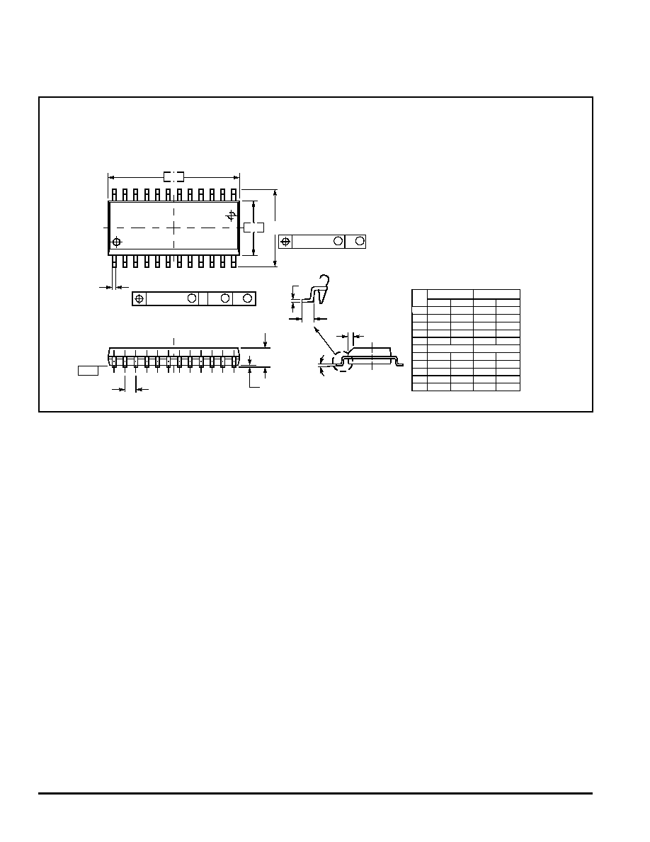
PACKAGE DIMENSIONS
DW SUFFIX
(24-LEAD SOIC WIDE BODY)
PLASTIC PACKAGE
CASE 751E-04
ISSUE E
NOTES:
1.
DIMENSIONING AND TOLERANCING PER ANSI
Y14.5M, 1982.
2.
CONTROLLING DIMENSION: MILLIMETER.
3.
DIMENSIONS A AND B DO NOT INCLUDE MOLD
PROTRUSION.
4.
MAXIMUM MOLD PROTRUSION 0.15 (0.006) PER
SIDE.
5.
DIMENSION D DOES NOT INCLUDE DAMBAR
PROTRUSION. ALLOWABLE DAMBAR
PROTRUSION SHALL BE 0.13 (0.005) TOTAL IN
EXCESS OF D DIMENSION AT MAXIMUM MATERIAL
CONDITION.
-A-
-B-
P
12X
D
24X
12
13
24
1
M
0.010 (0.25)
B
M
S
A
M
0.010 (0.25)
B
S
T
-T-
G
22X
SEATING
PLANE
K
C
R
X 45
∞
M
F
J
DIM
MIN
MAX
MIN
MAX
INCHES
MILLIMETERS
A
15.25
15.54
0.601
0.612
B
7.40
7.60
0.292
0.299
C
2.35
2.65
0.093
0.104
D
0.35
0.49
0.014
0.019
F
0.41
0.90
0.016
0.035
G
1.27 BSC
0.050 BSC
J
0.23
0.32
0.009
0.013
K
0.13
0.29
0.005
0.011
M
0
8
0
8
P
10.05
10.55
0.395
0.415
R
0.25
0.75
0.010
0.029
◊
◊
◊
◊
F
r
e
e
s
c
a
l
e
S
e
m
i
c
o
n
d
u
c
t
o
r
,
I
Freescale Semiconductor, Inc.
For More Information On This Product,
Go to: www.freescale.com
n
c
.
.
.

MOTOROLA ANALOG INTEGRATED CIRCUIT DEVICE DATA
33397
17
NOTES
F
r
e
e
s
c
a
l
e
S
e
m
i
c
o
n
d
u
c
t
o
r
,
I
Freescale Semiconductor, Inc.
For More Information On This Product,
Go to: www.freescale.com
n
c
.
.
.

33397
MOTOROLA ANALOG INTEGRATED CIRCUIT DEVICE DATA
18
NOTES
F
r
e
e
s
c
a
l
e
S
e
m
i
c
o
n
d
u
c
t
o
r
,
I
Freescale Semiconductor, Inc.
For More Information On This Product,
Go to: www.freescale.com
n
c
.
.
.

MOTOROLA ANALOG INTEGRATED CIRCUIT DEVICE DATA
33397
19
NOTES
F
r
e
e
s
c
a
l
e
S
e
m
i
c
o
n
d
u
c
t
o
r
,
I
Freescale Semiconductor, Inc.
For More Information On This Product,
Go to: www.freescale.com
n
c
.
.
.

HOW TO REACH US:
USA/EUROPE/LOCATIONS NOT LISTED:
JAPAN: Motorola Japan Ltd.; SPS, Technical Information Center
Motorola Literature Distribution
3-20-1 Minami-Azabu. Minato-ku, Tokyo 106-8573, Japan
P.O. Box 5405, Denver, Colorado 80217
81-3-3440-3569
1-800-521-6274 or 480-768-2130
ASIA/PACIFIC: Motorola Semiconductors H.K. Ltd.; Silicon Harbour Centre
2 Dai King Street, Tai Po Industrial Estate, Tai Po, N.T., Hong Kong
852-26668334
HOME PAGE: http://motorola.com/semiconductors
MC33397/D
Information in this document is provided solely to enable system and software implementers to use Motorola products. There are no express or implied
copyright licenses granted hereunder to design or fabricate any integrated circuits or integrated circuits based on the information in this document.
Motorola reserves the right to make changes without further notice to any products herein. Motorola makes no warranty, representation or guarantee
regarding the suitability of its products for any particular purpose, nor does Motorola assume any liability arising out of the application or use of any product
or circuit, and specifically disclaims any and all liability, including without limitation consequential or incidental damages. "Typical" parameters which may be
provided in Motorola data sheets and/or specifications can and do vary in different applications and actual performance may vary over time. All operating
parameters, including "Typicals" must be validated for each customer application by customer's technical experts. Motorola does not convey any license
under its patent rights nor the rights of others. Motorola products are not designed, intended, or authorized for use as components in systems intended for
surgical implant into the body, or other applications intended to support or sustain life, or for any other application in which the failure of the Motorola product
could create a situation where personal injury or death may occur. Should Buyer purchase or use Motorola products for any such unintended or
unauthorized application, Buyer shall indemnify and hold Motorola and its officers, employees, subsidiaries, affiliates, and distributors harmless against all
claims, costs, damages, and expenses, and reasonable attorney fees arising out of, directly or indirectly, any claim of personal injury or death associated
with such unintended or unauthorized use, even if such claim alleges that Motorola was negligent regarding the design or manufacture of the part.
MOTOROLA and the Stylized M Logo are registered in the US Patent and Trademark Office. All other product or service names are the property of their
respective owners.
© Motorola, Inc. 2003
F
r
e
e
s
c
a
l
e
S
e
m
i
c
o
n
d
u
c
t
o
r
,
I
Freescale Semiconductor, Inc.
For More Information On This Product,
Go to: www.freescale.com
n
c
.
.
.