
M68HC08
Microcontrollers
freescale.com
MC68HC908LB8
Data Sheet
MC68HC908LB8
Rev. 0
2/2005

MC68HC908LB8 Data Sheet, Rev. 0
Freescale Semiconductor
3
MC68HC908LB8
Data Sheet
To provide the most up-to-date information, the revision of our documents on the World Wide Web will be
the most current. Your printed copy may be an earlier revision. To verify you have the latest information
available, refer to:
http://www.freescale.com
The following revision history table summarizes changes contained in this document. For your
convenience, the page number designators have been linked to the appropriate location.
Revision History
Date
Revision
Level
Description
Page
Number(s)
2
2
/2005
0
First release
N/A

MC68HC908LB8 Data Sheet, Rev. 0
4
Freescale Semiconductor

MC68HC908LB8 Data Sheet, Rev. 0
Freescale Semiconductor
5
List of Sections
Chapter 1
General Description . . . . . . . . . . . . . . . . . . . . . . . . . . . . . . . . . . . . . . . . . . . . . 17
Chapter 2
Memory . . . . . . . . . . . . . . . . . . . . . . . . . . . . . . . . . . . . . . . . . . . . . . . . . . . . . . . . 25
Chapter 3
Analog-to-Digital Converter (ADC). . . . . . . . . . . . . . . . . . . . . . . . . . . . . . . . . . 45
Chapter 4
Op Amp/Comparator Module . . . . . . . . . . . . . . . . . . . . . . . . . . . . . . . . . . . . . . 53
Chapter 5
Configuration Register (CONFIG) . . . . . . . . . . . . . . . . . . . . . . . . . . . . . . . . . . 57
Chapter 6
Computer Operating Properly (COP) Module . . . . . . . . . . . . . . . . . . . . . . . . . 61
Chapter 7
Central Processor Unit (CPU). . . . . . . . . . . . . . . . . . . . . . . . . . . . . . . . . . . . . . 65
Chapter 8
External Interrupt (IRQ) . . . . . . . . . . . . . . . . . . . . . . . . . . . . . . . . . . . . . . . . . . . 79
Chapter 9
Keyboard Interrupt Module (KBI) . . . . . . . . . . . . . . . . . . . . . . . . . . . . . . . . . . . 83
Chapter 10 High Resolution PWM (HRP) . . . . . . . . . . . . . . . . . . . . . . . . . . . . . . . . . . . . . . 89
Chapter 11 Low-Power Modes . . . . . . . . . . . . . . . . . . . . . . . . . . . . . . . . . . . . . . . . . . . . . . 111
Chapter 12 Low-Voltage Inhibit (LVI) . . . . . . . . . . . . . . . . . . . . . . . . . . . . . . . . . . . . . . . . 117
Chapter 13 Oscillator Module (OSC) . . . . . . . . . . . . . . . . . . . . . . . . . . . . . . . . . . . . . . . . . 121
Chapter 14 Input/Output (I/O) Ports. . . . . . . . . . . . . . . . . . . . . . . . . . . . . . . . . . . . . . . . . . 131
Chapter 15 Pulse Width Modulator with Fault Input (PWM) . . . . . . . . . . . . . . . . . . . . . . 139
Chapter 16 Resets and Interrupts . . . . . . . . . . . . . . . . . . . . . . . . . . . . . . . . . . . . . . . . . . . 161
Chapter 17 System Integration Module (SIM) . . . . . . . . . . . . . . . . . . . . . . . . . . . . . . . . . . 169
Chapter 18 Timer Interface Module (TIM) . . . . . . . . . . . . . . . . . . . . . . . . . . . . . . . . . . . . . 185
Chapter 19 Development Support . . . . . . . . . . . . . . . . . . . . . . . . . . . . . . . . . . . . . . . . . . . 201
Chapter 20 Electrical Specifications . . . . . . . . . . . . . . . . . . . . . . . . . . . . . . . . . . . . . . . . . 219
Chapter 21 Ordering Information and Mechanical Specifications . . . . . . . . . . . . . . . . . 229

MC68HC908LB8 Data Sheet
6
Freescale Semiconductor

MC68HC908LB8 Data Sheet, Rev. 0
Freescale Semiconductor
7
Table of Contents
Chapter 1
General Description
1.1
Introduction . . . . . . . . . . . . . . . . . . . . . . . . . . . . . . . . . . . . . . . . . . . . . . . . . . . . . . . . . . . . . . . . 17
1.2
Features . . . . . . . . . . . . . . . . . . . . . . . . . . . . . . . . . . . . . . . . . . . . . . . . . . . . . . . . . . . . . . . . . . . 17
1.2.1
Standard Features of the MC68HC908LB8 . . . . . . . . . . . . . . . . . . . . . . . . . . . . . . . . . . . . . 17
1.2.2
Features of the CPU08 . . . . . . . . . . . . . . . . . . . . . . . . . . . . . . . . . . . . . . . . . . . . . . . . . . . . 19
1.3
MCU Block Diagram . . . . . . . . . . . . . . . . . . . . . . . . . . . . . . . . . . . . . . . . . . . . . . . . . . . . . . . . . 19
1.4
Pin Assignments . . . . . . . . . . . . . . . . . . . . . . . . . . . . . . . . . . . . . . . . . . . . . . . . . . . . . . . . . . . . 20
1.5
Pin Functions . . . . . . . . . . . . . . . . . . . . . . . . . . . . . . . . . . . . . . . . . . . . . . . . . . . . . . . . . . . . . . . 21
1.6
Pin Function Priority . . . . . . . . . . . . . . . . . . . . . . . . . . . . . . . . . . . . . . . . . . . . . . . . . . . . . . . . . . 22
1.7
System Clock Distribution . . . . . . . . . . . . . . . . . . . . . . . . . . . . . . . . . . . . . . . . . . . . . . . . . . . . . 24
Chapter 2
Memory
2.1
Introduction . . . . . . . . . . . . . . . . . . . . . . . . . . . . . . . . . . . . . . . . . . . . . . . . . . . . . . . . . . . . . . . . 25
2.2
Unimplemented Memory Locations . . . . . . . . . . . . . . . . . . . . . . . . . . . . . . . . . . . . . . . . . . . . . . 25
2.3
Reserved Memory Locations . . . . . . . . . . . . . . . . . . . . . . . . . . . . . . . . . . . . . . . . . . . . . . . . . . . 25
2.4
Register Section. . . . . . . . . . . . . . . . . . . . . . . . . . . . . . . . . . . . . . . . . . . . . . . . . . . . . . . . . . . . . 25
2.5
Random-Access Memory (RAM) . . . . . . . . . . . . . . . . . . . . . . . . . . . . . . . . . . . . . . . . . . . . . . . . 35
2.6
FLASH Memory (FLASH) . . . . . . . . . . . . . . . . . . . . . . . . . . . . . . . . . . . . . . . . . . . . . . . . . . . . . 36
2.6.1
FLASH Control Register. . . . . . . . . . . . . . . . . . . . . . . . . . . . . . . . . . . . . . . . . . . . . . . . . . . . 37
2.6.2
FLASH Page Erase Operation . . . . . . . . . . . . . . . . . . . . . . . . . . . . . . . . . . . . . . . . . . . . . . . 37
2.6.3
FLASH Mass Erase Operation. . . . . . . . . . . . . . . . . . . . . . . . . . . . . . . . . . . . . . . . . . . . . . . 38
2.6.4
FLASH Program/Read Operation . . . . . . . . . . . . . . . . . . . . . . . . . . . . . . . . . . . . . . . . . . . . 39
2.6.5
FLASH Block Protection. . . . . . . . . . . . . . . . . . . . . . . . . . . . . . . . . . . . . . . . . . . . . . . . . . . . 40
2.6.6
FLASH Block Protect Register . . . . . . . . . . . . . . . . . . . . . . . . . . . . . . . . . . . . . . . . . . . . . . . 42
2.6.7
Wait Mode . . . . . . . . . . . . . . . . . . . . . . . . . . . . . . . . . . . . . . . . . . . . . . . . . . . . . . . . . . . . . . 43
2.6.8
Stop Mode . . . . . . . . . . . . . . . . . . . . . . . . . . . . . . . . . . . . . . . . . . . . . . . . . . . . . . . . . . . . . . 43
Chapter 3
Analog-to-Digital Converter (ADC)
3.1
Introduction . . . . . . . . . . . . . . . . . . . . . . . . . . . . . . . . . . . . . . . . . . . . . . . . . . . . . . . . . . . . . . . . 45
3.2
Features . . . . . . . . . . . . . . . . . . . . . . . . . . . . . . . . . . . . . . . . . . . . . . . . . . . . . . . . . . . . . . . . . . . 46
3.3
Functional Description . . . . . . . . . . . . . . . . . . . . . . . . . . . . . . . . . . . . . . . . . . . . . . . . . . . . . . . . 46
3.3.1
ADC Port I/O Pins . . . . . . . . . . . . . . . . . . . . . . . . . . . . . . . . . . . . . . . . . . . . . . . . . . . . . . . . 46
3.3.2
Voltage Conversion . . . . . . . . . . . . . . . . . . . . . . . . . . . . . . . . . . . . . . . . . . . . . . . . . . . . . . . 47
3.3.3
Conversion Time . . . . . . . . . . . . . . . . . . . . . . . . . . . . . . . . . . . . . . . . . . . . . . . . . . . . . . . . . 47
3.3.4
Conversion . . . . . . . . . . . . . . . . . . . . . . . . . . . . . . . . . . . . . . . . . . . . . . . . . . . . . . . . . . . . . . 47
3.3.5
Accuracy and Precision . . . . . . . . . . . . . . . . . . . . . . . . . . . . . . . . . . . . . . . . . . . . . . . . . . . . 47
3.4
Monotonicity . . . . . . . . . . . . . . . . . . . . . . . . . . . . . . . . . . . . . . . . . . . . . . . . . . . . . . . . . . . . . . . . 47

MC68HC908LB8 Data Sheet
8
Freescale Semiconductor
3.5
Interrupts . . . . . . . . . . . . . . . . . . . . . . . . . . . . . . . . . . . . . . . . . . . . . . . . . . . . . . . . . . . . . . . . . . 47
3.6
Low-Power Modes . . . . . . . . . . . . . . . . . . . . . . . . . . . . . . . . . . . . . . . . . . . . . . . . . . . . . . . . . . . 48
3.6.1
Wait Mode . . . . . . . . . . . . . . . . . . . . . . . . . . . . . . . . . . . . . . . . . . . . . . . . . . . . . . . . . . . . . . 48
3.6.2
Stop Mode . . . . . . . . . . . . . . . . . . . . . . . . . . . . . . . . . . . . . . . . . . . . . . . . . . . . . . . . . . . . . . 48
3.7
I/O Signals . . . . . . . . . . . . . . . . . . . . . . . . . . . . . . . . . . . . . . . . . . . . . . . . . . . . . . . . . . . . . . . . . 48
3.8
I/O Registers . . . . . . . . . . . . . . . . . . . . . . . . . . . . . . . . . . . . . . . . . . . . . . . . . . . . . . . . . . . . . . . 48
3.8.1
ADC Status and Control Register . . . . . . . . . . . . . . . . . . . . . . . . . . . . . . . . . . . . . . . . . . . . 48
3.8.2
ADC Data Register. . . . . . . . . . . . . . . . . . . . . . . . . . . . . . . . . . . . . . . . . . . . . . . . . . . . . . . . 50
3.8.3
ADC Clock Register . . . . . . . . . . . . . . . . . . . . . . . . . . . . . . . . . . . . . . . . . . . . . . . . . . . . . . . 50
Chapter 4
Op Amp/Comparator Module
4.1
Introduction . . . . . . . . . . . . . . . . . . . . . . . . . . . . . . . . . . . . . . . . . . . . . . . . . . . . . . . . . . . . . . . . 53
4.2
Features . . . . . . . . . . . . . . . . . . . . . . . . . . . . . . . . . . . . . . . . . . . . . . . . . . . . . . . . . . . . . . . . . . . 53
4.3
Pin Name Conventions . . . . . . . . . . . . . . . . . . . . . . . . . . . . . . . . . . . . . . . . . . . . . . . . . . . . . . . 53
4.4
Functional Description . . . . . . . . . . . . . . . . . . . . . . . . . . . . . . . . . . . . . . . . . . . . . . . . . . . . . . . . 54
4.5
Low Power Modes . . . . . . . . . . . . . . . . . . . . . . . . . . . . . . . . . . . . . . . . . . . . . . . . . . . . . . . . . . . 55
4.5.1
Wait Mode . . . . . . . . . . . . . . . . . . . . . . . . . . . . . . . . . . . . . . . . . . . . . . . . . . . . . . . . . . . . . . 55
4.5.2
Stop Mode . . . . . . . . . . . . . . . . . . . . . . . . . . . . . . . . . . . . . . . . . . . . . . . . . . . . . . . . . . . . . . 55
4.6
Op Amp/Comparator Control Register . . . . . . . . . . . . . . . . . . . . . . . . . . . . . . . . . . . . . . . . . . . . 55
Chapter 5
Configuration Register (CONFIG)
5.1
Introduction . . . . . . . . . . . . . . . . . . . . . . . . . . . . . . . . . . . . . . . . . . . . . . . . . . . . . . . . . . . . . . . . 57
5.2
Functional Description . . . . . . . . . . . . . . . . . . . . . . . . . . . . . . . . . . . . . . . . . . . . . . . . . . . . . . . . 57
Chapter 6
Computer Operating Properly (COP) Module
6.1
Introduction . . . . . . . . . . . . . . . . . . . . . . . . . . . . . . . . . . . . . . . . . . . . . . . . . . . . . . . . . . . . . . . . 61
6.2
Functional Description . . . . . . . . . . . . . . . . . . . . . . . . . . . . . . . . . . . . . . . . . . . . . . . . . . . . . . . . 61
6.3
I/O Signals . . . . . . . . . . . . . . . . . . . . . . . . . . . . . . . . . . . . . . . . . . . . . . . . . . . . . . . . . . . . . . . . . 62
6.3.1
BUSCLKX4 . . . . . . . . . . . . . . . . . . . . . . . . . . . . . . . . . . . . . . . . . . . . . . . . . . . . . . . . . . . . . 62
6.3.2
COPCTL Write . . . . . . . . . . . . . . . . . . . . . . . . . . . . . . . . . . . . . . . . . . . . . . . . . . . . . . . . . . . 62
6.3.3
Power-On Reset. . . . . . . . . . . . . . . . . . . . . . . . . . . . . . . . . . . . . . . . . . . . . . . . . . . . . . . . . . 62
6.3.4
Internal Reset. . . . . . . . . . . . . . . . . . . . . . . . . . . . . . . . . . . . . . . . . . . . . . . . . . . . . . . . . . . . 62
6.3.5
Reset Vector Fetch . . . . . . . . . . . . . . . . . . . . . . . . . . . . . . . . . . . . . . . . . . . . . . . . . . . . . . . 62
6.3.6
COPD (COP Disable). . . . . . . . . . . . . . . . . . . . . . . . . . . . . . . . . . . . . . . . . . . . . . . . . . . . . . 63
6.3.7
COPRS (COP Rate Select) . . . . . . . . . . . . . . . . . . . . . . . . . . . . . . . . . . . . . . . . . . . . . . . . . 63
6.4
COP Control Register . . . . . . . . . . . . . . . . . . . . . . . . . . . . . . . . . . . . . . . . . . . . . . . . . . . . . . . . 63
6.5
Interrupts . . . . . . . . . . . . . . . . . . . . . . . . . . . . . . . . . . . . . . . . . . . . . . . . . . . . . . . . . . . . . . . . . . 63
6.6
Monitor Mode . . . . . . . . . . . . . . . . . . . . . . . . . . . . . . . . . . . . . . . . . . . . . . . . . . . . . . . . . . . . . . . 63
6.7
Low-Power Modes . . . . . . . . . . . . . . . . . . . . . . . . . . . . . . . . . . . . . . . . . . . . . . . . . . . . . . . . . . . 63
6.7.1
Wait Mode . . . . . . . . . . . . . . . . . . . . . . . . . . . . . . . . . . . . . . . . . . . . . . . . . . . . . . . . . . . . . . 63
6.7.2
Stop Mode . . . . . . . . . . . . . . . . . . . . . . . . . . . . . . . . . . . . . . . . . . . . . . . . . . . . . . . . . . . . . . 63

MC68HC908LB8 Data Sheet
Freescale Semiconductor
9
Chapter 7
Central Processor Unit (CPU)
7.1
Introduction . . . . . . . . . . . . . . . . . . . . . . . . . . . . . . . . . . . . . . . . . . . . . . . . . . . . . . . . . . . . . . . . 65
7.2
Features . . . . . . . . . . . . . . . . . . . . . . . . . . . . . . . . . . . . . . . . . . . . . . . . . . . . . . . . . . . . . . . . . . . 65
7.3
CPU Registers . . . . . . . . . . . . . . . . . . . . . . . . . . . . . . . . . . . . . . . . . . . . . . . . . . . . . . . . . . . . . . 65
7.3.1
Accumulator . . . . . . . . . . . . . . . . . . . . . . . . . . . . . . . . . . . . . . . . . . . . . . . . . . . . . . . . . . . . . 66
7.3.2
Index Register . . . . . . . . . . . . . . . . . . . . . . . . . . . . . . . . . . . . . . . . . . . . . . . . . . . . . . . . . . . 66
7.3.3
Stack Pointer . . . . . . . . . . . . . . . . . . . . . . . . . . . . . . . . . . . . . . . . . . . . . . . . . . . . . . . . . . . . 67
7.3.4
Program Counter . . . . . . . . . . . . . . . . . . . . . . . . . . . . . . . . . . . . . . . . . . . . . . . . . . . . . . . . . 67
7.3.5
Condition Code Register . . . . . . . . . . . . . . . . . . . . . . . . . . . . . . . . . . . . . . . . . . . . . . . . . . . 67
7.4
Arithmetic/Logic Unit (ALU) . . . . . . . . . . . . . . . . . . . . . . . . . . . . . . . . . . . . . . . . . . . . . . . . . . . . 69
7.5
Low-Power Modes . . . . . . . . . . . . . . . . . . . . . . . . . . . . . . . . . . . . . . . . . . . . . . . . . . . . . . . . . . . 69
7.5.1
Wait Mode . . . . . . . . . . . . . . . . . . . . . . . . . . . . . . . . . . . . . . . . . . . . . . . . . . . . . . . . . . . . . . 69
7.5.2
Stop Mode . . . . . . . . . . . . . . . . . . . . . . . . . . . . . . . . . . . . . . . . . . . . . . . . . . . . . . . . . . . . . . 69
7.6
CPU During Break Interrupts . . . . . . . . . . . . . . . . . . . . . . . . . . . . . . . . . . . . . . . . . . . . . . . . . . . 69
7.7
Instruction Set Summary . . . . . . . . . . . . . . . . . . . . . . . . . . . . . . . . . . . . . . . . . . . . . . . . . . . . . . 70
7.8
Opcode Map . . . . . . . . . . . . . . . . . . . . . . . . . . . . . . . . . . . . . . . . . . . . . . . . . . . . . . . . . . . . . . . 76
Chapter 8
External Interrupt (IRQ)
8.1
Introduction . . . . . . . . . . . . . . . . . . . . . . . . . . . . . . . . . . . . . . . . . . . . . . . . . . . . . . . . . . . . . . . . 79
8.2
Features . . . . . . . . . . . . . . . . . . . . . . . . . . . . . . . . . . . . . . . . . . . . . . . . . . . . . . . . . . . . . . . . . . . 79
8.3
Functional Description . . . . . . . . . . . . . . . . . . . . . . . . . . . . . . . . . . . . . . . . . . . . . . . . . . . . . . . . 79
8.4
IRQ Pin . . . . . . . . . . . . . . . . . . . . . . . . . . . . . . . . . . . . . . . . . . . . . . . . . . . . . . . . . . . . . . . . . . . 80
8.5
IRQ Module During Break Interrupts . . . . . . . . . . . . . . . . . . . . . . . . . . . . . . . . . . . . . . . . . . . . . 81
8.6
IRQ Status and Control Register . . . . . . . . . . . . . . . . . . . . . . . . . . . . . . . . . . . . . . . . . . . . . . . . 81
Chapter 9
Keyboard Interrupt Module (KBI)
9.1
Introduction . . . . . . . . . . . . . . . . . . . . . . . . . . . . . . . . . . . . . . . . . . . . . . . . . . . . . . . . . . . . . . . . 83
9.2
Features . . . . . . . . . . . . . . . . . . . . . . . . . . . . . . . . . . . . . . . . . . . . . . . . . . . . . . . . . . . . . . . . . . . 84
9.3
Functional Description . . . . . . . . . . . . . . . . . . . . . . . . . . . . . . . . . . . . . . . . . . . . . . . . . . . . . . . . 85
9.4
Keyboard Initialization . . . . . . . . . . . . . . . . . . . . . . . . . . . . . . . . . . . . . . . . . . . . . . . . . . . . . . . . 86
9.5
Low-Power Modes . . . . . . . . . . . . . . . . . . . . . . . . . . . . . . . . . . . . . . . . . . . . . . . . . . . . . . . . . . . 86
9.5.1
Wait Mode . . . . . . . . . . . . . . . . . . . . . . . . . . . . . . . . . . . . . . . . . . . . . . . . . . . . . . . . . . . . . . 86
9.5.2
Stop Mode . . . . . . . . . . . . . . . . . . . . . . . . . . . . . . . . . . . . . . . . . . . . . . . . . . . . . . . . . . . . . . 86
9.6
Keyboard Module During Break Interrupts. . . . . . . . . . . . . . . . . . . . . . . . . . . . . . . . . . . . . . . . . 86
9.7
I/O Registers . . . . . . . . . . . . . . . . . . . . . . . . . . . . . . . . . . . . . . . . . . . . . . . . . . . . . . . . . . . . . . . 87
9.7.1
Keyboard Status and Control Register. . . . . . . . . . . . . . . . . . . . . . . . . . . . . . . . . . . . . . . . . 87
9.7.2
Keyboard Interrupt Enable Register. . . . . . . . . . . . . . . . . . . . . . . . . . . . . . . . . . . . . . . . . . . 87
Chapter 10
High Resolution PWM (HRP)
10.1
Introduction . . . . . . . . . . . . . . . . . . . . . . . . . . . . . . . . . . . . . . . . . . . . . . . . . . . . . . . . . . . . . . . . 89
10.2
Features . . . . . . . . . . . . . . . . . . . . . . . . . . . . . . . . . . . . . . . . . . . . . . . . . . . . . . . . . . . . . . . . . . . 89

MC68HC908LB8 Data Sheet
10
Freescale Semiconductor
10.3
Pin Name Conventions . . . . . . . . . . . . . . . . . . . . . . . . . . . . . . . . . . . . . . . . . . . . . . . . . . . . . . . 89
10.4
Functional Description . . . . . . . . . . . . . . . . . . . . . . . . . . . . . . . . . . . . . . . . . . . . . . . . . . . . . . . . 91
10.4.1
The Principle of Frequency Dithering. . . . . . . . . . . . . . . . . . . . . . . . . . . . . . . . . . . . . . . . . . 92
10.4.2
Frequency Dithering on the HRP . . . . . . . . . . . . . . . . . . . . . . . . . . . . . . . . . . . . . . . . . . . . . 93
10.4.3
Duty Cycle Dithering . . . . . . . . . . . . . . . . . . . . . . . . . . . . . . . . . . . . . . . . . . . . . . . . . . . . . . 94
10.4.4
Frequency Generation . . . . . . . . . . . . . . . . . . . . . . . . . . . . . . . . . . . . . . . . . . . . . . . . . . . . . 94
10.4.5
Variable Frequency Mode (HRPMODE = 0) . . . . . . . . . . . . . . . . . . . . . . . . . . . . . . . . . . . . 97
10.4.6
Variable Duty Cycle Mode (HRPMODE = 1) . . . . . . . . . . . . . . . . . . . . . . . . . . . . . . . . . . . . 97
10.4.7
Dithering Controller . . . . . . . . . . . . . . . . . . . . . . . . . . . . . . . . . . . . . . . . . . . . . . . . . . . . . . . 98
10.4.8
Dithering Controller Timebase . . . . . . . . . . . . . . . . . . . . . . . . . . . . . . . . . . . . . . . . . . . . . . . 99
10.4.9
Deadtime Insertion . . . . . . . . . . . . . . . . . . . . . . . . . . . . . . . . . . . . . . . . . . . . . . . . . . . . . . . . 99
10.5
Interrupts . . . . . . . . . . . . . . . . . . . . . . . . . . . . . . . . . . . . . . . . . . . . . . . . . . . . . . . . . . . . . . . . . 102
10.6
Low-Power Modes . . . . . . . . . . . . . . . . . . . . . . . . . . . . . . . . . . . . . . . . . . . . . . . . . . . . . . . . . . 102
10.6.1
Wait Mode . . . . . . . . . . . . . . . . . . . . . . . . . . . . . . . . . . . . . . . . . . . . . . . . . . . . . . . . . . . . . 102
10.6.2
Stop Mode . . . . . . . . . . . . . . . . . . . . . . . . . . . . . . . . . . . . . . . . . . . . . . . . . . . . . . . . . . . . . 102
10.7
HRP During Break Interrupts . . . . . . . . . . . . . . . . . . . . . . . . . . . . . . . . . . . . . . . . . . . . . . . . . . 102
10.7.1
Input/Output Signals. . . . . . . . . . . . . . . . . . . . . . . . . . . . . . . . . . . . . . . . . . . . . . . . . . . . . . 102
10.8
HRP Registers . . . . . . . . . . . . . . . . . . . . . . . . . . . . . . . . . . . . . . . . . . . . . . . . . . . . . . . . . . . . . 103
10.8.1
HRP Control Register. . . . . . . . . . . . . . . . . . . . . . . . . . . . . . . . . . . . . . . . . . . . . . . . . . . . . 103
10.8.2
HRP Duty Cycle Registers . . . . . . . . . . . . . . . . . . . . . . . . . . . . . . . . . . . . . . . . . . . . . . . . . 104
10.8.3
HRP Period Registers . . . . . . . . . . . . . . . . . . . . . . . . . . . . . . . . . . . . . . . . . . . . . . . . . . . . 105
10.8.4
HRP Deadtime Register. . . . . . . . . . . . . . . . . . . . . . . . . . . . . . . . . . . . . . . . . . . . . . . . . . . 106
10.8.5
Frequency Dithering HRP Timebase Registers . . . . . . . . . . . . . . . . . . . . . . . . . . . . . . . . . 106
10.8.6
Frequency Dithering Control Register . . . . . . . . . . . . . . . . . . . . . . . . . . . . . . . . . . . . . . . . 107
10.9
HRP Programming Examples . . . . . . . . . . . . . . . . . . . . . . . . . . . . . . . . . . . . . . . . . . . . . . . . . 108
Chapter 11
Low-Power Modes
11.1
Introduction . . . . . . . . . . . . . . . . . . . . . . . . . . . . . . . . . . . . . . . . . . . . . . . . . . . . . . . . . . . . . . . 111
11.1.1
Wait Mode . . . . . . . . . . . . . . . . . . . . . . . . . . . . . . . . . . . . . . . . . . . . . . . . . . . . . . . . . . . . . 111
11.1.2
Stop Mode . . . . . . . . . . . . . . . . . . . . . . . . . . . . . . . . . . . . . . . . . . . . . . . . . . . . . . . . . . . . . 111
11.2
Analog-to-Digital Converter (ADC). . . . . . . . . . . . . . . . . . . . . . . . . . . . . . . . . . . . . . . . . . . . . . 111
11.2.1
Wait Mode . . . . . . . . . . . . . . . . . . . . . . . . . . . . . . . . . . . . . . . . . . . . . . . . . . . . . . . . . . . . . 111
11.2.2
Stop Mode . . . . . . . . . . . . . . . . . . . . . . . . . . . . . . . . . . . . . . . . . . . . . . . . . . . . . . . . . . . . . 111
11.3
Break Module (BRK) . . . . . . . . . . . . . . . . . . . . . . . . . . . . . . . . . . . . . . . . . . . . . . . . . . . . . . . . 111
11.3.1
Wait Mode . . . . . . . . . . . . . . . . . . . . . . . . . . . . . . . . . . . . . . . . . . . . . . . . . . . . . . . . . . . . . 111
11.3.2
Stop Mode . . . . . . . . . . . . . . . . . . . . . . . . . . . . . . . . . . . . . . . . . . . . . . . . . . . . . . . . . . . . . 112
11.4
Central Processor Unit (CPU) . . . . . . . . . . . . . . . . . . . . . . . . . . . . . . . . . . . . . . . . . . . . . . . . . 112
11.4.1
Wait Mode . . . . . . . . . . . . . . . . . . . . . . . . . . . . . . . . . . . . . . . . . . . . . . . . . . . . . . . . . . . . . 112
11.4.2
Stop Mode . . . . . . . . . . . . . . . . . . . . . . . . . . . . . . . . . . . . . . . . . . . . . . . . . . . . . . . . . . . . . 112
11.5
Computer Operating Properly Module (COP) . . . . . . . . . . . . . . . . . . . . . . . . . . . . . . . . . . . . . 112
11.5.1
Wait Mode . . . . . . . . . . . . . . . . . . . . . . . . . . . . . . . . . . . . . . . . . . . . . . . . . . . . . . . . . . . . . 112
11.5.2
Stop Mode . . . . . . . . . . . . . . . . . . . . . . . . . . . . . . . . . . . . . . . . . . . . . . . . . . . . . . . . . . . . . 112
11.6
External Interrupt Module (IRQ) . . . . . . . . . . . . . . . . . . . . . . . . . . . . . . . . . . . . . . . . . . . . . . . . 112
11.6.1
Wait Mode . . . . . . . . . . . . . . . . . . . . . . . . . . . . . . . . . . . . . . . . . . . . . . . . . . . . . . . . . . . . . 112
11.6.2
Stop Mode . . . . . . . . . . . . . . . . . . . . . . . . . . . . . . . . . . . . . . . . . . . . . . . . . . . . . . . . . . . . . 112
11.7
Keyboard Interrupt Module (KBI) . . . . . . . . . . . . . . . . . . . . . . . . . . . . . . . . . . . . . . . . . . . . . . . 113

MC68HC908LB8 Data Sheet
Freescale Semiconductor
11
11.7.1
Wait Mode . . . . . . . . . . . . . . . . . . . . . . . . . . . . . . . . . . . . . . . . . . . . . . . . . . . . . . . . . . . . . 113
11.7.2
Stop Mode . . . . . . . . . . . . . . . . . . . . . . . . . . . . . . . . . . . . . . . . . . . . . . . . . . . . . . . . . . . . . 113
11.8
High Resolution PWM (HRP) . . . . . . . . . . . . . . . . . . . . . . . . . . . . . . . . . . . . . . . . . . . . . . . . . . 113
11.8.1
Wait Mode . . . . . . . . . . . . . . . . . . . . . . . . . . . . . . . . . . . . . . . . . . . . . . . . . . . . . . . . . . . . . 113
11.8.2
Stop Mode . . . . . . . . . . . . . . . . . . . . . . . . . . . . . . . . . . . . . . . . . . . . . . . . . . . . . . . . . . . . . 113
11.9
Low-Voltage Inhibit Module (LVI) . . . . . . . . . . . . . . . . . . . . . . . . . . . . . . . . . . . . . . . . . . . . . . . 113
11.9.1
Wait Mode . . . . . . . . . . . . . . . . . . . . . . . . . . . . . . . . . . . . . . . . . . . . . . . . . . . . . . . . . . . . . 113
11.9.2
Stop Mode . . . . . . . . . . . . . . . . . . . . . . . . . . . . . . . . . . . . . . . . . . . . . . . . . . . . . . . . . . . . . 113
11.10 Op Amp/Comparator . . . . . . . . . . . . . . . . . . . . . . . . . . . . . . . . . . . . . . . . . . . . . . . . . . . . . . . . 114
11.10.1
Wait Mode . . . . . . . . . . . . . . . . . . . . . . . . . . . . . . . . . . . . . . . . . . . . . . . . . . . . . . . . . . . . . 114
11.10.2
Stop Mode . . . . . . . . . . . . . . . . . . . . . . . . . . . . . . . . . . . . . . . . . . . . . . . . . . . . . . . . . . . . . 114
11.11 Oscillator Module (OSC) . . . . . . . . . . . . . . . . . . . . . . . . . . . . . . . . . . . . . . . . . . . . . . . . . . . . . 114
11.11.1
Wait Mode . . . . . . . . . . . . . . . . . . . . . . . . . . . . . . . . . . . . . . . . . . . . . . . . . . . . . . . . . . . . . 114
11.11.2
Stop Mode . . . . . . . . . . . . . . . . . . . . . . . . . . . . . . . . . . . . . . . . . . . . . . . . . . . . . . . . . . . . . 114
11.12 Pulse-Width Modulator Module (PWM) . . . . . . . . . . . . . . . . . . . . . . . . . . . . . . . . . . . . . . . . . . 114
11.12.1
Wait Mode . . . . . . . . . . . . . . . . . . . . . . . . . . . . . . . . . . . . . . . . . . . . . . . . . . . . . . . . . . . . . 114
11.12.2
Stop Mode . . . . . . . . . . . . . . . . . . . . . . . . . . . . . . . . . . . . . . . . . . . . . . . . . . . . . . . . . . . . . 114
11.13 Timer Interface Module (TIM) . . . . . . . . . . . . . . . . . . . . . . . . . . . . . . . . . . . . . . . . . . . . . . . . . 115
11.13.1
Wait Mode . . . . . . . . . . . . . . . . . . . . . . . . . . . . . . . . . . . . . . . . . . . . . . . . . . . . . . . . . . . . . 115
11.13.2
Stop Mode . . . . . . . . . . . . . . . . . . . . . . . . . . . . . . . . . . . . . . . . . . . . . . . . . . . . . . . . . . . . . 115
11.14 Exiting Wait Mode . . . . . . . . . . . . . . . . . . . . . . . . . . . . . . . . . . . . . . . . . . . . . . . . . . . . . . . . . . 115
11.15 Exiting Stop Mode . . . . . . . . . . . . . . . . . . . . . . . . . . . . . . . . . . . . . . . . . . . . . . . . . . . . . . . . . . 116
Chapter 12
Low-Voltage Inhibit (LVI)
12.1
Introduction . . . . . . . . . . . . . . . . . . . . . . . . . . . . . . . . . . . . . . . . . . . . . . . . . . . . . . . . . . . . . . . 117
12.2
Features . . . . . . . . . . . . . . . . . . . . . . . . . . . . . . . . . . . . . . . . . . . . . . . . . . . . . . . . . . . . . . . . . . 117
12.3
Functional Description . . . . . . . . . . . . . . . . . . . . . . . . . . . . . . . . . . . . . . . . . . . . . . . . . . . . . . . 117
12.3.1
Polled LVI Operation . . . . . . . . . . . . . . . . . . . . . . . . . . . . . . . . . . . . . . . . . . . . . . . . . . . . . 118
12.3.2
Forced Reset Operation. . . . . . . . . . . . . . . . . . . . . . . . . . . . . . . . . . . . . . . . . . . . . . . . . . . 118
12.3.3
Voltage Hysteresis Protection . . . . . . . . . . . . . . . . . . . . . . . . . . . . . . . . . . . . . . . . . . . . . . 118
12.4
LVI Status Register . . . . . . . . . . . . . . . . . . . . . . . . . . . . . . . . . . . . . . . . . . . . . . . . . . . . . . . . . 119
12.5
LVI Interrupts . . . . . . . . . . . . . . . . . . . . . . . . . . . . . . . . . . . . . . . . . . . . . . . . . . . . . . . . . . . . . . 119
12.6
Low-Power Modes . . . . . . . . . . . . . . . . . . . . . . . . . . . . . . . . . . . . . . . . . . . . . . . . . . . . . . . . . . 119
12.6.1
Wait Mode . . . . . . . . . . . . . . . . . . . . . . . . . . . . . . . . . . . . . . . . . . . . . . . . . . . . . . . . . . . . . 119
12.6.2
Stop Mode . . . . . . . . . . . . . . . . . . . . . . . . . . . . . . . . . . . . . . . . . . . . . . . . . . . . . . . . . . . . . 119
Chapter 13
Oscillator Module (OSC)
13.1
Introduction . . . . . . . . . . . . . . . . . . . . . . . . . . . . . . . . . . . . . . . . . . . . . . . . . . . . . . . . . . . . . . . 121
13.2
Features . . . . . . . . . . . . . . . . . . . . . . . . . . . . . . . . . . . . . . . . . . . . . . . . . . . . . . . . . . . . . . . . . . 121
13.3
Functional Description . . . . . . . . . . . . . . . . . . . . . . . . . . . . . . . . . . . . . . . . . . . . . . . . . . . . . . . 121
13.3.1
Internal Oscillator . . . . . . . . . . . . . . . . . . . . . . . . . . . . . . . . . . . . . . . . . . . . . . . . . . . . . . . . 122
13.3.1.1
Internal Oscillator Trimming . . . . . . . . . . . . . . . . . . . . . . . . . . . . . . . . . . . . . . . . . . . . . . 123
13.3.1.2
Internal to External Clock Switching . . . . . . . . . . . . . . . . . . . . . . . . . . . . . . . . . . . . . . . . 123
13.3.2
External Oscillator . . . . . . . . . . . . . . . . . . . . . . . . . . . . . . . . . . . . . . . . . . . . . . . . . . . . . . . 123

MC68HC908LB8 Data Sheet
12
Freescale Semiconductor
13.3.3
XTAL Oscillator . . . . . . . . . . . . . . . . . . . . . . . . . . . . . . . . . . . . . . . . . . . . . . . . . . . . . . . . . 124
13.3.4
RC Oscillator . . . . . . . . . . . . . . . . . . . . . . . . . . . . . . . . . . . . . . . . . . . . . . . . . . . . . . . . . . . 124
13.4
Oscillator Module Signals . . . . . . . . . . . . . . . . . . . . . . . . . . . . . . . . . . . . . . . . . . . . . . . . . . . . 126
13.4.1
Crystal Amplifier Input Pin (OSC1). . . . . . . . . . . . . . . . . . . . . . . . . . . . . . . . . . . . . . . . . . . 126
13.4.2
Crystal Amplifier Output Pin (OSC2/PTC1/BUSCLKX4) . . . . . . . . . . . . . . . . . . . . . . . . . . 126
13.4.3
Oscillator Enable Signal (SIMOSCEN) . . . . . . . . . . . . . . . . . . . . . . . . . . . . . . . . . . . . . . . 126
13.4.4
XTAL Oscillator Clock (XTALCLK). . . . . . . . . . . . . . . . . . . . . . . . . . . . . . . . . . . . . . . . . . . 126
13.4.5
RC Oscillator Clock (RCCLK) . . . . . . . . . . . . . . . . . . . . . . . . . . . . . . . . . . . . . . . . . . . . . . 126
13.4.6
Internal Oscillator Clock (INTCLK) . . . . . . . . . . . . . . . . . . . . . . . . . . . . . . . . . . . . . . . . . . . 127
13.4.7
Oscillator Out 2 (BUSCLKX4) . . . . . . . . . . . . . . . . . . . . . . . . . . . . . . . . . . . . . . . . . . . . . . 127
13.4.8
Oscillator Out (BUSCLKX2) . . . . . . . . . . . . . . . . . . . . . . . . . . . . . . . . . . . . . . . . . . . . . . . . 127
13.5
Low Power Modes . . . . . . . . . . . . . . . . . . . . . . . . . . . . . . . . . . . . . . . . . . . . . . . . . . . . . . . . . . 127
13.5.1
Wait Mode . . . . . . . . . . . . . . . . . . . . . . . . . . . . . . . . . . . . . . . . . . . . . . . . . . . . . . . . . . . . . 127
13.5.2
Stop Mode . . . . . . . . . . . . . . . . . . . . . . . . . . . . . . . . . . . . . . . . . . . . . . . . . . . . . . . . . . . . . 127
13.6
Oscillator During Break Mode . . . . . . . . . . . . . . . . . . . . . . . . . . . . . . . . . . . . . . . . . . . . . . . . . 127
13.7
CONFIG2 Options . . . . . . . . . . . . . . . . . . . . . . . . . . . . . . . . . . . . . . . . . . . . . . . . . . . . . . . . . . 127
13.8
Input/Output (I/O) Registers . . . . . . . . . . . . . . . . . . . . . . . . . . . . . . . . . . . . . . . . . . . . . . . . . . . 128
13.8.1
Oscillator Status Register. . . . . . . . . . . . . . . . . . . . . . . . . . . . . . . . . . . . . . . . . . . . . . . . . . 128
13.8.2
Oscillator Trim Register (OSCTRIM) . . . . . . . . . . . . . . . . . . . . . . . . . . . . . . . . . . . . . . . . . 129
Chapter 14
Input/Output (I/O) Ports
14.1
Introduction . . . . . . . . . . . . . . . . . . . . . . . . . . . . . . . . . . . . . . . . . . . . . . . . . . . . . . . . . . . . . . . 131
14.2
Port A . . . . . . . . . . . . . . . . . . . . . . . . . . . . . . . . . . . . . . . . . . . . . . . . . . . . . . . . . . . . . . . . . . . . 132
14.2.1
Port A Data Register . . . . . . . . . . . . . . . . . . . . . . . . . . . . . . . . . . . . . . . . . . . . . . . . . . . . . 132
14.2.2
Data Direction Register A . . . . . . . . . . . . . . . . . . . . . . . . . . . . . . . . . . . . . . . . . . . . . . . . . 132
14.2.3
Port A Input Pullup Enable Register. . . . . . . . . . . . . . . . . . . . . . . . . . . . . . . . . . . . . . . . . . 134
14.3
Port B . . . . . . . . . . . . . . . . . . . . . . . . . . . . . . . . . . . . . . . . . . . . . . . . . . . . . . . . . . . . . . . . . . . . 134
14.3.1
Port B Data Register . . . . . . . . . . . . . . . . . . . . . . . . . . . . . . . . . . . . . . . . . . . . . . . . . . . . . 134
14.3.2
Data Direction Register B . . . . . . . . . . . . . . . . . . . . . . . . . . . . . . . . . . . . . . . . . . . . . . . . . 135
14.4
Port C. . . . . . . . . . . . . . . . . . . . . . . . . . . . . . . . . . . . . . . . . . . . . . . . . . . . . . . . . . . . . . . . . . . . 136
14.4.1
Port C Data Register . . . . . . . . . . . . . . . . . . . . . . . . . . . . . . . . . . . . . . . . . . . . . . . . . . . . . 136
14.4.2
Data Direction Register C . . . . . . . . . . . . . . . . . . . . . . . . . . . . . . . . . . . . . . . . . . . . . . . . . 136
14.4.3
Port C Input Pullup Enable Register . . . . . . . . . . . . . . . . . . . . . . . . . . . . . . . . . . . . . . . . . 138
Chapter 15
Pulse Width Modulator with Fault Input (PWM)
15.1
Introduction . . . . . . . . . . . . . . . . . . . . . . . . . . . . . . . . . . . . . . . . . . . . . . . . . . . . . . . . . . . . . . . 139
15.2
Features . . . . . . . . . . . . . . . . . . . . . . . . . . . . . . . . . . . . . . . . . . . . . . . . . . . . . . . . . . . . . . . . . . 139
15.3
Timebase . . . . . . . . . . . . . . . . . . . . . . . . . . . . . . . . . . . . . . . . . . . . . . . . . . . . . . . . . . . . . . . . . 142
15.3.1
Resolution . . . . . . . . . . . . . . . . . . . . . . . . . . . . . . . . . . . . . . . . . . . . . . . . . . . . . . . . . . . . . 142
15.3.2
Prescaler . . . . . . . . . . . . . . . . . . . . . . . . . . . . . . . . . . . . . . . . . . . . . . . . . . . . . . . . . . . . . . 143
15.4
PWM Generators . . . . . . . . . . . . . . . . . . . . . . . . . . . . . . . . . . . . . . . . . . . . . . . . . . . . . . . . . . . 144
15.4.1
Load Operation . . . . . . . . . . . . . . . . . . . . . . . . . . . . . . . . . . . . . . . . . . . . . . . . . . . . . . . . . 144
15.4.2
PWM Data Overflow and Underflow Conditions . . . . . . . . . . . . . . . . . . . . . . . . . . . . . . . . 146
15.4.3
Output Polarity . . . . . . . . . . . . . . . . . . . . . . . . . . . . . . . . . . . . . . . . . . . . . . . . . . . . . . . . . . 147
15.5
Fault Protection . . . . . . . . . . . . . . . . . . . . . . . . . . . . . . . . . . . . . . . . . . . . . . . . . . . . . . . . . . . . 147

MC68HC908LB8 Data Sheet
Freescale Semiconductor
13
15.5.1
Fault Condition Input Pin . . . . . . . . . . . . . . . . . . . . . . . . . . . . . . . . . . . . . . . . . . . . . . . . . . 147
15.5.1.1
Automatic Mode . . . . . . . . . . . . . . . . . . . . . . . . . . . . . . . . . . . . . . . . . . . . . . . . . . . . . . . 148
15.5.1.2
Manual Mode . . . . . . . . . . . . . . . . . . . . . . . . . . . . . . . . . . . . . . . . . . . . . . . . . . . . . . . . . 149
15.5.2
Software Output Disable . . . . . . . . . . . . . . . . . . . . . . . . . . . . . . . . . . . . . . . . . . . . . . . . . . 149
15.6
Initialization and the PWMEN Bit . . . . . . . . . . . . . . . . . . . . . . . . . . . . . . . . . . . . . . . . . . . . . . . 150
15.7
PWM Operation in Low-Power Modes . . . . . . . . . . . . . . . . . . . . . . . . . . . . . . . . . . . . . . . . . . . 150
15.7.1
Wait Mode . . . . . . . . . . . . . . . . . . . . . . . . . . . . . . . . . . . . . . . . . . . . . . . . . . . . . . . . . . . . . 150
15.7.2
Stop Mode . . . . . . . . . . . . . . . . . . . . . . . . . . . . . . . . . . . . . . . . . . . . . . . . . . . . . . . . . . . . . 151
15.8
Control Logic Block . . . . . . . . . . . . . . . . . . . . . . . . . . . . . . . . . . . . . . . . . . . . . . . . . . . . . . . . . 151
15.8.1
PWM Counter Registers . . . . . . . . . . . . . . . . . . . . . . . . . . . . . . . . . . . . . . . . . . . . . . . . . . 151
15.8.2
PWM Counter Modulo Registers . . . . . . . . . . . . . . . . . . . . . . . . . . . . . . . . . . . . . . . . . . . . 151
15.8.3
PWMx Value Registers . . . . . . . . . . . . . . . . . . . . . . . . . . . . . . . . . . . . . . . . . . . . . . . . . . . 152
15.8.4
PWM Control Register 1 . . . . . . . . . . . . . . . . . . . . . . . . . . . . . . . . . . . . . . . . . . . . . . . . . . 153
15.8.5
PWM Control Register 2 . . . . . . . . . . . . . . . . . . . . . . . . . . . . . . . . . . . . . . . . . . . . . . . . . . 154
15.8.6
PWM Disable Mapping Write-Once Register . . . . . . . . . . . . . . . . . . . . . . . . . . . . . . . . . . . 156
15.8.7
Fault Control Register . . . . . . . . . . . . . . . . . . . . . . . . . . . . . . . . . . . . . . . . . . . . . . . . . . . . 157
15.8.8
Fault Status Register . . . . . . . . . . . . . . . . . . . . . . . . . . . . . . . . . . . . . . . . . . . . . . . . . . . . . 157
15.8.9
Fault Control Register 2 . . . . . . . . . . . . . . . . . . . . . . . . . . . . . . . . . . . . . . . . . . . . . . . . . . . 158
15.9
PWM Glossary . . . . . . . . . . . . . . . . . . . . . . . . . . . . . . . . . . . . . . . . . . . . . . . . . . . . . . . . . . . . . 158
Chapter 16
Resets and Interrupts
16.1
Introduction . . . . . . . . . . . . . . . . . . . . . . . . . . . . . . . . . . . . . . . . . . . . . . . . . . . . . . . . . . . . . . . 161
16.2
Resets . . . . . . . . . . . . . . . . . . . . . . . . . . . . . . . . . . . . . . . . . . . . . . . . . . . . . . . . . . . . . . . . . . . 161
16.2.1
Effects . . . . . . . . . . . . . . . . . . . . . . . . . . . . . . . . . . . . . . . . . . . . . . . . . . . . . . . . . . . . . . . . 161
16.2.2
External Reset . . . . . . . . . . . . . . . . . . . . . . . . . . . . . . . . . . . . . . . . . . . . . . . . . . . . . . . . . . 161
16.2.3
Internal Reset. . . . . . . . . . . . . . . . . . . . . . . . . . . . . . . . . . . . . . . . . . . . . . . . . . . . . . . . . . . 161
16.2.3.1
Power-On Reset (POR) . . . . . . . . . . . . . . . . . . . . . . . . . . . . . . . . . . . . . . . . . . . . . . . . . 161
16.2.3.2
Computer Operating Properly (COP) Reset . . . . . . . . . . . . . . . . . . . . . . . . . . . . . . . . . . 162
16.2.3.3
Low-Voltage Inhibit (LVI) Reset . . . . . . . . . . . . . . . . . . . . . . . . . . . . . . . . . . . . . . . . . . . 162
16.2.3.4
Illegal Opcode Reset . . . . . . . . . . . . . . . . . . . . . . . . . . . . . . . . . . . . . . . . . . . . . . . . . . . 162
16.2.3.5
Illegal Address Reset . . . . . . . . . . . . . . . . . . . . . . . . . . . . . . . . . . . . . . . . . . . . . . . . . . . 162
16.2.4
System Integration Module (SIM) Reset Status Register. . . . . . . . . . . . . . . . . . . . . . . . . . 163
16.3
Interrupts . . . . . . . . . . . . . . . . . . . . . . . . . . . . . . . . . . . . . . . . . . . . . . . . . . . . . . . . . . . . . . . . . 164
16.3.1
Effects . . . . . . . . . . . . . . . . . . . . . . . . . . . . . . . . . . . . . . . . . . . . . . . . . . . . . . . . . . . . . . . . 164
16.3.2
Sources . . . . . . . . . . . . . . . . . . . . . . . . . . . . . . . . . . . . . . . . . . . . . . . . . . . . . . . . . . . . . . . 165
16.3.2.1
Software Interrupt (SWI) Instruction . . . . . . . . . . . . . . . . . . . . . . . . . . . . . . . . . . . . . . . . 167
16.3.2.2
Break Interrupt . . . . . . . . . . . . . . . . . . . . . . . . . . . . . . . . . . . . . . . . . . . . . . . . . . . . . . . . 168
16.3.2.3
IRQ Pin . . . . . . . . . . . . . . . . . . . . . . . . . . . . . . . . . . . . . . . . . . . . . . . . . . . . . . . . . . . . . . 168
16.3.2.4
Timer Interface Module (TIM) . . . . . . . . . . . . . . . . . . . . . . . . . . . . . . . . . . . . . . . . . . . . . 168
16.3.2.5
KBD0≠KBD6 Pins. . . . . . . . . . . . . . . . . . . . . . . . . . . . . . . . . . . . . . . . . . . . . . . . . . . . . . 168
16.3.2.6
Analog-to-Digital Converter (ADC) . . . . . . . . . . . . . . . . . . . . . . . . . . . . . . . . . . . . . . . . . 168
16.3.2.7
Pulse-Width Modulator with Fault Input (PWM) . . . . . . . . . . . . . . . . . . . . . . . . . . . . . . . 168
16.3.2.8
High Resolution PWM (HRP) . . . . . . . . . . . . . . . . . . . . . . . . . . . . . . . . . . . . . . . . . . . . . 168

MC68HC908LB8 Data Sheet
14
Freescale Semiconductor
Chapter 17
System Integration Module (SIM)
17.1
Introduction . . . . . . . . . . . . . . . . . . . . . . . . . . . . . . . . . . . . . . . . . . . . . . . . . . . . . . . . . . . . . . . 169
17.2
SIM Bus Clock Control and Generation . . . . . . . . . . . . . . . . . . . . . . . . . . . . . . . . . . . . . . . . . . 171
17.2.1
Bus Timing . . . . . . . . . . . . . . . . . . . . . . . . . . . . . . . . . . . . . . . . . . . . . . . . . . . . . . . . . . . . . 171
17.2.2
Clock Start-Up from POR. . . . . . . . . . . . . . . . . . . . . . . . . . . . . . . . . . . . . . . . . . . . . . . . . . 171
17.2.3
Clocks in Stop Mode and Wait Mode . . . . . . . . . . . . . . . . . . . . . . . . . . . . . . . . . . . . . . . . . 171
17.3
Reset and System Initialization . . . . . . . . . . . . . . . . . . . . . . . . . . . . . . . . . . . . . . . . . . . . . . . . 172
17.3.1
External Pin Reset . . . . . . . . . . . . . . . . . . . . . . . . . . . . . . . . . . . . . . . . . . . . . . . . . . . . . . . 172
17.3.2
Active Resets from Internal Sources . . . . . . . . . . . . . . . . . . . . . . . . . . . . . . . . . . . . . . . . . 172
17.3.2.1
Power-On Reset . . . . . . . . . . . . . . . . . . . . . . . . . . . . . . . . . . . . . . . . . . . . . . . . . . . . . . . 173
17.3.2.2
Computer Operating Properly (COP) Reset . . . . . . . . . . . . . . . . . . . . . . . . . . . . . . . . . . 174
17.3.2.3
Illegal Opcode Reset . . . . . . . . . . . . . . . . . . . . . . . . . . . . . . . . . . . . . . . . . . . . . . . . . . . 174
17.3.2.4
Illegal Address Reset . . . . . . . . . . . . . . . . . . . . . . . . . . . . . . . . . . . . . . . . . . . . . . . . . . . 174
17.3.2.5
Low-Voltage Inhibit (LVI) Reset . . . . . . . . . . . . . . . . . . . . . . . . . . . . . . . . . . . . . . . . . . . 174
17.3.2.6
Monitor Mode Entry Module Reset (MODRST) . . . . . . . . . . . . . . . . . . . . . . . . . . . . . . . 175
17.4
SIM Counter . . . . . . . . . . . . . . . . . . . . . . . . . . . . . . . . . . . . . . . . . . . . . . . . . . . . . . . . . . . . . . . 175
17.4.1
SIM Counter During Power-On Reset . . . . . . . . . . . . . . . . . . . . . . . . . . . . . . . . . . . . . . . . 175
17.4.2
SIM Counter During Stop Mode Recovery. . . . . . . . . . . . . . . . . . . . . . . . . . . . . . . . . . . . . 175
17.4.3
SIM Counter and Reset States . . . . . . . . . . . . . . . . . . . . . . . . . . . . . . . . . . . . . . . . . . . . . 175
17.5
Exception Control. . . . . . . . . . . . . . . . . . . . . . . . . . . . . . . . . . . . . . . . . . . . . . . . . . . . . . . . . . . 175
17.5.1
Interrupts . . . . . . . . . . . . . . . . . . . . . . . . . . . . . . . . . . . . . . . . . . . . . . . . . . . . . . . . . . . . . . 175
17.5.1.1
Hardware Interrupts . . . . . . . . . . . . . . . . . . . . . . . . . . . . . . . . . . . . . . . . . . . . . . . . . . . . 176
17.5.1.2
SWI Instruction . . . . . . . . . . . . . . . . . . . . . . . . . . . . . . . . . . . . . . . . . . . . . . . . . . . . . . . . 178
17.5.2
Reset . . . . . . . . . . . . . . . . . . . . . . . . . . . . . . . . . . . . . . . . . . . . . . . . . . . . . . . . . . . . . . . . . 178
17.5.3
Break Interrupts . . . . . . . . . . . . . . . . . . . . . . . . . . . . . . . . . . . . . . . . . . . . . . . . . . . . . . . . . 178
17.5.4
Status Flag Protection in Break Mode . . . . . . . . . . . . . . . . . . . . . . . . . . . . . . . . . . . . . . . . 179
17.6
Low-Power Modes . . . . . . . . . . . . . . . . . . . . . . . . . . . . . . . . . . . . . . . . . . . . . . . . . . . . . . . . . . 179
17.6.1
Wait Mode . . . . . . . . . . . . . . . . . . . . . . . . . . . . . . . . . . . . . . . . . . . . . . . . . . . . . . . . . . . . . 179
17.6.2
Stop Mode . . . . . . . . . . . . . . . . . . . . . . . . . . . . . . . . . . . . . . . . . . . . . . . . . . . . . . . . . . . . . 180
17.7
SIM Registers . . . . . . . . . . . . . . . . . . . . . . . . . . . . . . . . . . . . . . . . . . . . . . . . . . . . . . . . . . . . . 181
17.7.1
Break Status Register . . . . . . . . . . . . . . . . . . . . . . . . . . . . . . . . . . . . . . . . . . . . . . . . . . . . 181
17.7.2
SIM Reset Status Register . . . . . . . . . . . . . . . . . . . . . . . . . . . . . . . . . . . . . . . . . . . . . . . . 182
17.7.3
Break Flag Control Register . . . . . . . . . . . . . . . . . . . . . . . . . . . . . . . . . . . . . . . . . . . . . . . 183
Chapter 18
Timer Interface Module (TIM)
18.1
Introduction . . . . . . . . . . . . . . . . . . . . . . . . . . . . . . . . . . . . . . . . . . . . . . . . . . . . . . . . . . . . . . . 185
18.2
Features . . . . . . . . . . . . . . . . . . . . . . . . . . . . . . . . . . . . . . . . . . . . . . . . . . . . . . . . . . . . . . . . . . 186
18.3
Functional Description . . . . . . . . . . . . . . . . . . . . . . . . . . . . . . . . . . . . . . . . . . . . . . . . . . . . . . . 186
18.3.1
TIM Counter Prescaler . . . . . . . . . . . . . . . . . . . . . . . . . . . . . . . . . . . . . . . . . . . . . . . . . . . . 188
18.3.2
Input Capture . . . . . . . . . . . . . . . . . . . . . . . . . . . . . . . . . . . . . . . . . . . . . . . . . . . . . . . . . . . 188
18.3.3
Output Compare. . . . . . . . . . . . . . . . . . . . . . . . . . . . . . . . . . . . . . . . . . . . . . . . . . . . . . . . . 188
18.3.3.1
Unbuffered Output Compare . . . . . . . . . . . . . . . . . . . . . . . . . . . . . . . . . . . . . . . . . . . . . 188
18.3.3.2
Buffered Output Compare . . . . . . . . . . . . . . . . . . . . . . . . . . . . . . . . . . . . . . . . . . . . . . . 189
18.3.4
Pulse Width Modulation (PWM) . . . . . . . . . . . . . . . . . . . . . . . . . . . . . . . . . . . . . . . . . . . . . 189
18.3.4.1
Unbuffered PWM Signal Generation . . . . . . . . . . . . . . . . . . . . . . . . . . . . . . . . . . . . . . . 190

MC68HC908LB8 Data Sheet
Freescale Semiconductor
15
18.3.4.2
Buffered PWM Signal Generation . . . . . . . . . . . . . . . . . . . . . . . . . . . . . . . . . . . . . . . . . 190
18.3.4.3
PWM Initialization . . . . . . . . . . . . . . . . . . . . . . . . . . . . . . . . . . . . . . . . . . . . . . . . . . . . . . 191
18.4
Interrupts . . . . . . . . . . . . . . . . . . . . . . . . . . . . . . . . . . . . . . . . . . . . . . . . . . . . . . . . . . . . . . . . . 191
18.5
Low-Power Modes . . . . . . . . . . . . . . . . . . . . . . . . . . . . . . . . . . . . . . . . . . . . . . . . . . . . . . . . . . 192
18.5.1
Wait Mode . . . . . . . . . . . . . . . . . . . . . . . . . . . . . . . . . . . . . . . . . . . . . . . . . . . . . . . . . . . . . 192
18.5.2
Stop Mode . . . . . . . . . . . . . . . . . . . . . . . . . . . . . . . . . . . . . . . . . . . . . . . . . . . . . . . . . . . . . 192
18.6
TIM During Break Interrupts. . . . . . . . . . . . . . . . . . . . . . . . . . . . . . . . . . . . . . . . . . . . . . . . . . . 192
18.7
I/O Signals . . . . . . . . . . . . . . . . . . . . . . . . . . . . . . . . . . . . . . . . . . . . . . . . . . . . . . . . . . . . . . . . 192
18.8
I/O Registers . . . . . . . . . . . . . . . . . . . . . . . . . . . . . . . . . . . . . . . . . . . . . . . . . . . . . . . . . . . . . . 193
18.8.1
TIM Status and Control Register . . . . . . . . . . . . . . . . . . . . . . . . . . . . . . . . . . . . . . . . . . . . 193
18.8.2
TIM Counter Registers . . . . . . . . . . . . . . . . . . . . . . . . . . . . . . . . . . . . . . . . . . . . . . . . . . . . 194
18.8.3
TIM Counter Modulo Registers . . . . . . . . . . . . . . . . . . . . . . . . . . . . . . . . . . . . . . . . . . . . . 195
18.8.4
TIM Channel Status and Control Registers . . . . . . . . . . . . . . . . . . . . . . . . . . . . . . . . . . . . 195
18.8.5
TIM Channel Registers . . . . . . . . . . . . . . . . . . . . . . . . . . . . . . . . . . . . . . . . . . . . . . . . . . . 199
Chapter 19
Development Support
19.1
Introduction . . . . . . . . . . . . . . . . . . . . . . . . . . . . . . . . . . . . . . . . . . . . . . . . . . . . . . . . . . . . . . . 201
19.2
Break Module (BRK) . . . . . . . . . . . . . . . . . . . . . . . . . . . . . . . . . . . . . . . . . . . . . . . . . . . . . . . . 201
19.2.1
Functional Description . . . . . . . . . . . . . . . . . . . . . . . . . . . . . . . . . . . . . . . . . . . . . . . . . . . . 201
19.2.1.1
Flag Protection During Break Interrupts . . . . . . . . . . . . . . . . . . . . . . . . . . . . . . . . . . . . . 202
19.2.1.2
CPU During Break Interrupts . . . . . . . . . . . . . . . . . . . . . . . . . . . . . . . . . . . . . . . . . . . . . 203
19.2.1.3
TIM During Break Interrupts . . . . . . . . . . . . . . . . . . . . . . . . . . . . . . . . . . . . . . . . . . . . . . 203
19.2.1.4
COP During Break Interrupts . . . . . . . . . . . . . . . . . . . . . . . . . . . . . . . . . . . . . . . . . . . . . 203
19.2.2
Break Module Registers. . . . . . . . . . . . . . . . . . . . . . . . . . . . . . . . . . . . . . . . . . . . . . . . . . . 203
19.2.2.1
Break Status and Control Register . . . . . . . . . . . . . . . . . . . . . . . . . . . . . . . . . . . . . . . . . 203
19.2.2.2
Break Address Registers . . . . . . . . . . . . . . . . . . . . . . . . . . . . . . . . . . . . . . . . . . . . . . . . 204
19.2.2.3
Break Auxiliary Register . . . . . . . . . . . . . . . . . . . . . . . . . . . . . . . . . . . . . . . . . . . . . . . . . 204
19.2.2.4
Break Status Register. . . . . . . . . . . . . . . . . . . . . . . . . . . . . . . . . . . . . . . . . . . . . . . . . . . 204
19.2.2.5
Break Flag Control Register . . . . . . . . . . . . . . . . . . . . . . . . . . . . . . . . . . . . . . . . . . . . . 205
19.2.3
Low-Power Modes . . . . . . . . . . . . . . . . . . . . . . . . . . . . . . . . . . . . . . . . . . . . . . . . . . . . . . . 205
19.3
Monitor Module (MON) . . . . . . . . . . . . . . . . . . . . . . . . . . . . . . . . . . . . . . . . . . . . . . . . . . . . . . 206
19.3.1
Functional Description . . . . . . . . . . . . . . . . . . . . . . . . . . . . . . . . . . . . . . . . . . . . . . . . . . . . 206
19.3.1.1
Normal Monitor Mode . . . . . . . . . . . . . . . . . . . . . . . . . . . . . . . . . . . . . . . . . . . . . . . . . . . 212
19.3.1.2
Forced Monitor Mode . . . . . . . . . . . . . . . . . . . . . . . . . . . . . . . . . . . . . . . . . . . . . . . . . . . 212
19.3.1.3
Monitor Vectors . . . . . . . . . . . . . . . . . . . . . . . . . . . . . . . . . . . . . . . . . . . . . . . . . . . . . . . 212
19.3.1.4
Data Format . . . . . . . . . . . . . . . . . . . . . . . . . . . . . . . . . . . . . . . . . . . . . . . . . . . . . . . . . . 213
19.3.1.5
Break Signal . . . . . . . . . . . . . . . . . . . . . . . . . . . . . . . . . . . . . . . . . . . . . . . . . . . . . . . . . . 213
19.3.1.6
Baud Rate. . . . . . . . . . . . . . . . . . . . . . . . . . . . . . . . . . . . . . . . . . . . . . . . . . . . . . . . . . . . 213
19.3.1.7
Commands . . . . . . . . . . . . . . . . . . . . . . . . . . . . . . . . . . . . . . . . . . . . . . . . . . . . . . . . . . . 213
19.3.2
Security . . . . . . . . . . . . . . . . . . . . . . . . . . . . . . . . . . . . . . . . . . . . . . . . . . . . . . . . . . . . . . . 217
Chapter 20
Electrical Specifications
20.1
Introduction . . . . . . . . . . . . . . . . . . . . . . . . . . . . . . . . . . . . . . . . . . . . . . . . . . . . . . . . . . . . . . . 219
20.2
Absolute Maximum Ratings . . . . . . . . . . . . . . . . . . . . . . . . . . . . . . . . . . . . . . . . . . . . . . . . . . . 219
20.3
Functional Operating Range . . . . . . . . . . . . . . . . . . . . . . . . . . . . . . . . . . . . . . . . . . . . . . . . . . 220

MC68HC908LB8 Data Sheet
16
Freescale Semiconductor
20.4
Thermal Characteristics . . . . . . . . . . . . . . . . . . . . . . . . . . . . . . . . . . . . . . . . . . . . . . . . . . . . . . 220
20.5
5.0-Volt Electrical Characteristics . . . . . . . . . . . . . . . . . . . . . . . . . . . . . . . . . . . . . . . . . . . . . . 220
20.6
5.0-Volt Control Timing . . . . . . . . . . . . . . . . . . . . . . . . . . . . . . . . . . . . . . . . . . . . . . . . . . . . . . 221
20.7
Oscillator Characteristics . . . . . . . . . . . . . . . . . . . . . . . . . . . . . . . . . . . . . . . . . . . . . . . . . . . . . 222
20.8
5.0-Volt ADC Characteristics . . . . . . . . . . . . . . . . . . . . . . . . . . . . . . . . . . . . . . . . . . . . . . . . . . 223
20.9
Op Amp Parameters . . . . . . . . . . . . . . . . . . . . . . . . . . . . . . . . . . . . . . . . . . . . . . . . . . . . . . . . 224
20.10 Comparator Parameters . . . . . . . . . . . . . . . . . . . . . . . . . . . . . . . . . . . . . . . . . . . . . . . . . . . . . 224
20.11 Timer Interface Module Characteristics . . . . . . . . . . . . . . . . . . . . . . . . . . . . . . . . . . . . . . . . . . 225
20.12 Memory Characteristics . . . . . . . . . . . . . . . . . . . . . . . . . . . . . . . . . . . . . . . . . . . . . . . . . . . . . . 226
Chapter 21
Ordering Information and Mechanical Specifications
21.1
Introduction . . . . . . . . . . . . . . . . . . . . . . . . . . . . . . . . . . . . . . . . . . . . . . . . . . . . . . . . . . . . . . . 229
21.2
MC Order Numbers . . . . . . . . . . . . . . . . . . . . . . . . . . . . . . . . . . . . . . . . . . . . . . . . . . . . . . . . . 229
21.3
20-Pin Small Outline Integrated Circuit (SOIC) Package -- Case #751D . . . . . . . . . . . . . . . . 230
21.4
20-Pin Plastic Dual In-Line Package (PDIP) -- Case #738 . . . . . . . . . . . . . . . . . . . . . . . . . . . 230

MC68HC908LB8 Data Sheet, Rev. 0
Freescale Semiconductor
17
Chapter 1
General Description
1.1 Introduction
The MC68HC908LB8 is a member of the low-cost, high-performance M68HC08 Family of 8-bit
microcontroller units (MCUs). All MCUs in the family use the enhanced M68HC08 central processor unit
(CPU08) and are available with a variety of modules, memory sizes, memory types, and package types.
The MC68HC908LB8 has peripherals dedicated to high resolution PWM and power factor correction
(PFC).
1.2 Features
For convenience, features have been organized to reflect:
∑
Standard features of the MC68HC908LB8
∑
Features of the CPU08
1.2.1 Standard Features of the MC68HC908LB8
Features of the MC68HC908LB8 include:
∑
8-MHz internal bus frequency
∑
Trimmable internal oscillator:
≠
4.0 MHz internal bus operation
≠
8-bit trim capability
≠
25% untrimmed
≠
5% trimmed
∑
8 Kbytes of 10 K write/erase cycle typical on-chip in application programmable FLASH memory
with security option
(1)
∑
128 bytes of on-chip random-access memory (RAM)
∑
Dual channel high resolution PWM with dead time insertion and shutdown input. The outputs use
frequency dithering to achieve a 4 ns output resolution.
∑
Dual channel pulse-width modulator (PWM) module to provide power factor correction capability
∑
Seven channel, 8-bit successive approximation analog-to-digital converter (ADC)
∑
Op amp/comparator for power factor correction capability or general purpose use
∑
7-bit keyboard interrupt
∑
One 16-bit, 2-channel timer interface module with one output available on port pin (PTA6) for input
capture and PWM
∑
17 general-purpose input/output (I/O) pins and one input only pin
≠
Three shared with high resolution PWM (HRP)
≠
Three shared with PWM module
1. No security feature is absolutely secure. However, Freescale Semiconductor's strategy is to make reading or copying the
FLASH difficult for unauthorized users.

General Description
MC68HC908LB8 Data Sheet, Rev. 0
18
Freescale Semiconductor
≠
Three shared with op amp/comparator
≠
Seven shared with ADC module (AD[0:6])
≠
One shared with timer channel 0
≠
Two shared with OSC1 and OSC2
≠
One shared with reset
≠
Seven shared with keyboard interrupt
≠
One input-only pin shared with external interrupt (IRQ)
∑
Available packages:
≠
20-pin small outline integrated chip (SOIC) package
≠
20-pin plastic dual in-line package (PDIP)
∑
On-chip programming firmware for use with host personal computer which does not require high
voltage for entry
∑
System protection features:
≠
Optional computer operating properly (COP) reset
≠
Low-voltage reset
≠
Illegal opcode detection with reset
≠
Illegal address detection with reset
∑
Low-power design; fully static with stop and wait modes
∑
Standard low-power modes of operation:
≠
Wait mode
≠
Stop mode
∑
Master reset pin and power-on reset (POR)
∑
674 bytes of FLASH programming routines read-only memory (ROM)
∑
Break module (BRK) to allow single breakpoint setting during in-circuit debugging
∑
Internal pullup on RST pin to reduce customer system cost

MCU Block Diagram
MC68HC908LB8 Data Sheet, Rev. 0
Freescale Semiconductor
19
∑
Selectable pullups on ports A and C
≠
Selection on an individual port bit basis
≠
During output mode, pullups are disengaged
∑
High current 8-mA sink / 10-mA source capability on all port pins
1.2.2 Features of the CPU08
Features of the CPU08 include:
∑
Enhanced HC05 programming model
∑
Extensive loop control functions
∑
16 addressing modes (eight more than the HC05)
∑
16-bit index register and stack pointer
∑
Memory-to-memory data transfers
∑
Fast 8
◊ 8 multiply instruction
∑
Fast 16/8 divide instruction
∑
Binary coded decimal (BCD) instructions
∑
Optimization for controller applications
∑
Efficient C language support
1.3 MCU Block Diagram
Figure 1-1
shows the structure of the MC68HC908LB8.

General Description
MC68HC908LB8 Data Sheet, Rev. 0
20
Freescale Semiconductor
Figure 1-1. MCU Block Diagram
1.4 Pin Assignments
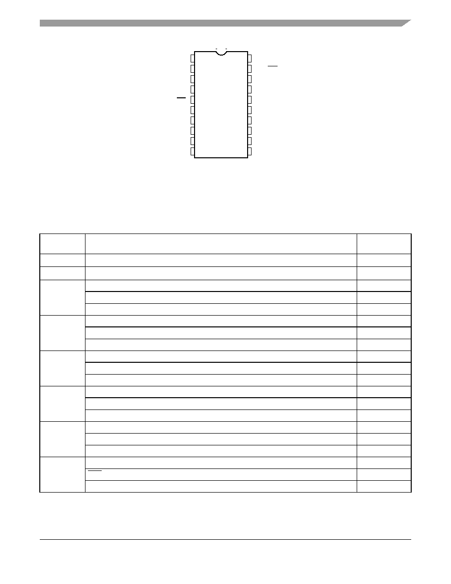
Figure 1-2
illustrates the pin assignments for the 20-pin SOIC package.
M68HC08 CPU
CONTROL AND STATUS
USER FLASH -- 8 KBYTES
USER RAM -- 128 BYTES
MONITOR ROM -- 350 BYTES
USER FLASH VECTOR SPACE -- 34 BYTES
DDRB
PORT
B
DDRC
PORTC
INTERNAL BUS
PTA6
(1)
/AD5/TCH0/KBI6
PTA5
(1)
/RST/KBI5
PTA4
(1)
/AD4/KBI4
PTA3
(1)
/AD3/KBI3
PTA2
(1)
/AD2/KBI2
PTA1
(1)
/AD1/KBI1
PTA0
(1)
/AD0/KBI0
PTB7/V
OUT
/AD6/FAULT
(2)
PTB6/V≠
PTB5/V+
PTB4/PWM1
PTB3/PWM0
PTB2/FAULT
(2)
PTB1/BOT
PTB0/TOP
PTC1
(1)
/OSC2
PTC0
(1)
/OSC1
POWER
V
SS
V
DD
DDRA
PORT
A
PTC2
(1)
/SHTDWN/IRQ
FLASH PROGRAMMING
OSCILLATOR
CPU
REGISTERS
ARITHMETIC/LOGIC
UNIT (ALU)
SYSTEM INTEGRATION
MODULE
DUAL CHANNEL PWM
MODULE
HIGH RESOLUTION PWM
MODULE
LOW-VOLTAGE INHIBIT
MODULE
COMPUTER OPERATING
PROPERLY MODULE
2-CHANNEL TIMER
MODULE
8-BIT ANALOG-TO-DIGITAL
CONVERTER MODULE
OP AMP/COMPARATOR
MODULE
KEYBOARD INTERRUPT
MODULE
MODULE
ROUTINES ROM -- 674 BYTES
REGISTERS -- 64 BYTES
1. Pin contains integrated pullup device.
2. Fault function switchable between pins PTB2 and PTB7.
Notes:
Pin Functions
MC68HC908LB8 Data Sheet, Rev. 0
Freescale Semiconductor
21
Figure 1-2. 20-Pin SOIC and PDIP Pin Assignments
1.5 Pin Functions
Table 1-1
provides a description of the pin functions.
Table 1-1. Pin Functions
Pin
Name
Description
Input/Output
V
DD
Power supply
Power
V
SS
Power supply ground
Power
PTA0
PTA0 -- General purpose I/O port
Input/Output
KBI0 -- Keyboard interrupt input 0
Input
ADC0 -- A/D channel 0 input
Input
PTA1
PTA1 -- General purpose I/O port
Input/Output
KBI1 -- Keyboard interrupt input 1
Input
ADC1 -- A/D channel 1 input
Input
PTA2
PTA2 -- General purpose I/O port
Input/Output
KBI2 -- Keyboard interrupt input 2
Input
ADC2 -- A/D channel 2 input
Input
PTA3
PTA3 -- General purpose I/O port
Input/Output
KBI3 -- Keyboard interrupt input 3
Input
ADC3 -- A/D channel 3 input
Input
PTA4
PTA4 -- General purpose I/O port
Input/Output
KBI4 -- Keyboard interrupt input 4
Input
ADC4 -- A/D channel 4 input
Input
PTA5
PTA5 -- General purpose I/O port
Input/Output
RST -- Reset input, active low with internal pullup and Schmitt trigger
Input
KBI5 -- Keyboard interrupt input 5
Input
1
2
3
4
5
6
7
8
9
10
20
19
18
17
16
15
14
13
12
11
V
DD
V
SS
PTC0/OSC1
PTC1/OSC2
PTC2/SHTDWN/IRQ
PTB0/TOP
PTB1/BOT
PTB2/FAULT
PTB3/PWM0
PTB4/PWM1
PTA6/ADC5/TCH0/KBI6
PTA5/RST/KBI5
PTA4/ADC4/KBI4
PTA3/ADC3/KBI3
PTA2/ADC2/KBI2
PTA1/ADC1/KBI1
PTA0/ADC0/KBI0
PTB7/V
OUT
/ADC6/FAULT
PTB6/V≠
PTB5/V+

General Description
MC68HC908LB8 Data Sheet, Rev. 0
22
Freescale Semiconductor
1.6 Pin Function Priority
Table 1-2
is meant to resolve the priority if multiple functions are enabled on a single pin.
NOTE
Upon reset all pins come up as input ports regardless of the priority table.
PTA6
PTA6 -- General purpose I/O port
Input/Output
KBI6 -- Keyboard interrupt input 6
Input
TCH0 -- Timer Channel 0 I/O
Input/Output
ADC5 -- A/D channel 5 input
Input
PTB0
PTB0 -- General purpose I/O port
Input/Output
TOP -- High resolution PWM output
Output
PTB1
PTB1 -- General purpose I/O port
Input/Output
BOT -- High resolution PWM output
Output
PTB2
PTB2 -- General purpose I/O port
Input/Output
FAULT -- High resolution PWM fault input (switchable between PTB2 and PTB7)
Input
PTB3
PTB3 -- General purpose I/O port
Input/Output
PWM0 -- Pulse-width modulator output 0
Output
PTB4
PTB4 -- General purpose I/O port
Input/Output
PWM1 -- Pulse-width modulator output 1
Output
PTB5
PTB5 -- General purpose I/O port
Input/Output
V+ -- Op amp/comparator input
Input
PTB6
PTB6 -- General purpose I/O port
Input/Output
V≠ -- Op amp/comparator input
Input
PTB7
PTB7 -- General purpose I/O port
Input/Output
V
OUT
-- Op amp/comparator output
Output
ADC6 -- A/D channel 6 input
Input
FAULT -- High resolution PWM fault input (switchable between PTB2 and PTB7)
Input
PTC0
PTC0 -- General purpose I/O port
Input/Output
OSC1 -- XTAL, RC, or external oscillator input
Input
PTC1
PTC1 -- General purpose I/O port
Input/Output
OSC2 -- XTAL oscillator output (XTAL option only)
RC or internal oscillator output (OSC2EN = 1 in PTAPUE register)
Output
Output
PTC2
PTC2 -- General purpose input port
Input
SHTDWN -- High resolution PWM input
Input
IRQ -- External interrupt with programmable pullup and Schmitt trigger
Input
Table 1-1. Pin Functions (Continued)
Pin
Name
Description
Input/Output

Pin Function Priority
MC68HC908LB8 Data Sheet, Rev. 0
Freescale Semiconductor
23
NOTE
Any unused inputs and I/O ports should be tied to an appropriate logic level
(either V
DD
or V
SS
). Although the I/O ports of the MC68HC908LB8 do not
require termination, termination is recommended to reduce the possibility
of static damage.
Table 1-2. Function Priority in Shared Pins
Pin Name
Highest-to-Lowest Priority Sequence
PTA0
ADC0
KBI0 PTA0
PTA1
ADC1
KBI1 PTA1
PTA2
ADC2
KBI2 PTA2
PTA3
ADC3
KBI3 PTA3
PTA4
ADC4
KBI4 PTA4
PTA5
RST
KBI5 PTA5
PTA6
ADC5
TCH0 KBI6 PTA6
PTB0
TOP
PTB0
PTB1
BOT
PTB1
PTB2
FAULT
(1)
PTB2
NOTES:
1. Fault function is switchable between pins PTB2 and PTB7.
2. V
OUT
, ADC6, and FAULT functions all share equal priority. All of these functions can be used
simultaneously on this pin.
PTB3
PWM0
PTB3
PTB4
PWM1
PTB4
PTB5
V+
PTB5
PTB6
V≠
PTB6
PTB7
V
OUT
/ ADC6 / FAULT
(1)(2)
PTB7
PTC0
OSC1
PTC0
PTC1
OSC2
PTC1
PTC2
SHTDWN
IRQ PTC2

General Description
MC68HC908LB8 Data Sheet, Rev. 0
24
Freescale Semiconductor
1.7 System Clock Distribution
Figure 1-3. System Clock Distribution Diagram
Some of the modules inside the MCU use different clock sources.
Figure 1-3
shows a simplified clock
connection diagram. The OSC supplies the clock sources:
∑
BUSCLKX4 is the basic reference clock of the device. It is either:
≠
The external crystal oscillator
≠
An external clock source
≠
An external RC oscillator
≠
The internal oscillator
PWM
FLASH
PROGRAMMING
ROM
HRP
COP
TIM
ADC
KBI
CPU
FLASH
RAM
MON ROM
OSC
BUSCLKX4
BUSCLKX4
BUSCLKX2
BUSCLK
˜2
˜4
SIM
MUX
IRC
V
DD
XRC
R
EXT

MC68HC908LB8 Data Sheet, Rev. 0
Freescale Semiconductor
25
Chapter 2
Memory
2.1 Introduction
The CPU08 can address 64 Kbytes of memory space. The memory map, shown in
Figure 2-1
, includes:
∑
System registers
∑
8192 bytes of user FLASH memory
∑
128 bytes of random-access memory (RAM)
∑
674 bytes of FLASH programming routines read-only memory (ROM)
∑
34 bytes of user-defined vectors
2.2 Unimplemented Memory Locations
Accessing an unimplemented location can cause an illegal address reset. In the memory map
(
Figure 2-1
) and in register figures in this document, unimplemented locations are shaded.
2.3 Reserved Memory Locations
Accessing a reserved location can have unpredictable effects on microcontroller (MCU) operation. In the
Figure 2-1
and in register figures in this document, reserved locations are marked with the word Reserved
or with the letter R.
2.4 Register Section
Most of the control, status, and data registers are in the zero page area of $0000≠$0058. Additional I/O
registers have these addresses:
∑
$FE00; break status register, BSR
∑
$FE01; SIM reset status register, SRSR
∑
$FE02; break auxiliary register, BRKAR
∑
$FE03; break flag control register, BFCR
∑
$FE04; interrupt status register 1, INT1
∑
$FE05; interrupt status register 2, INT2
∑
$FE06; reserved
∑
$FE07; reserved
∑
$FE08; FLASH control register, FLCR
∑
$FE09; break address register high, BRKH
∑
$FE0A; break address register low, BRKL
∑
$FE0B; break status and control register, BRKSCR
∑
$FE0C; LVI status register, LVISR
∑
$FF7E; FLASH block protect register, FLBPR

Memory
MC68HC908LB8 Data Sheet, Rev. 0
26
Freescale Semiconductor
Data registers are shown in
Figure 2-2
.
Table 2-1
is a list of vector locations.
$0000
I/O REGISTERS
$0058
$0059
UNIMPLEMENTED
(1)
$007F
$0080
RANDOM-ACCESS MEMORY
128 BYTES
$00FF
$0100
UNIMPLEMENTED
(1)
$037D
$037E
FLASH PROGRAMMING ROUTINES ROM
674 BYTES
$061F
$0620
$DEFF
UNIMPLEMENTED
(1)
$DE00
FLASH MEMORY
8192 BYTES
$FDFF
$FE00
BREAK STATUS REGISTER (BSR)
$FE01
SIM RESET STATUS REGISTER (SRSR)
$FE02
BREAK AUXILIARY REGISTER (BRKAR)
$FE03
BREAK FLAG CONTROL REGISTER (BFCR)
$FE04
INTERRUPT STATUS REGISTER 1 (INT1)
$FE05
INTERRUPT STATUS REGISTER 2 (INT2)
$FE06
RESERVED
$FE07
RESERVED
$FE08
FLASH CONTROL REGISTER (FLCR)
$FE09
BREAK ADDRESS REGISTER HIGH (BRKH)
$FE0A
BREAK ADDRESS REGISTER LOW (BRKL)
$FE0B
BREAK STATUS AND CONTROL REGISTER (BRKSCR)
$FE0C
LVI STATUS REGISTER (LVISR)
$FE0D
$FE1F
UNIMPLEMENTED
Figure 2-1. Memory Map

Register Section
MC68HC908LB8 Data Sheet, Rev. 0
Freescale Semiconductor
27
$FE20
MONITOR ROM
350 BYTES
$FF7D
$FF7E
FLASH BLOCK PROTECT REGISTER (FLBPR)
$FF7F
$FFBF
UNIMPLEMENTED
$FFC0
INTERNAL OSCILLATOR TRIM VALUE
$FFC1
$FFDD
UNIMPLEMENTED
$FFDE
$FFFF
(2)
FLASH VECTORS
34 BYTES
1. Attempts to execute code from addresses in these ranges will
generate an illegal address reset.
2. $FFF6≠$FFFD used for eight security bytes
Addr.
Register Name
Bit 7
6
5
4
3
2
1
Bit 0
$0000
Port A Data Register
(PTA)
See page 132.
Read:
PTA6
PTA5
PTA4
PTA3
PTA2
PTA1
PTA0
Write:
Reset:
Unaffected by reset
$0001
Port B Data Register
(PTB)
See page 134.
Read:
PTB7
PTB6
PTB5
PTB4
PTB3
PTB2
PTB1
PTB0
Write:
Reset:
Unaffected by reset
$0002
Port C Data Register
(PTC)
See page 136.
Read:
0
0
0
0
0
PTC2
PTC1
PTC0
Write:
Reset:
0
0
0
0
0
0
0
0
$0003
Reserved
Reserved
$0004
Data Direction Register A
(DDRA)
See page 133.
Read:
0
DDRA6
DDRA5
DDRA4
DDRA3
DDRA2
DDRA1
DDRA0
Write:
Reset:
0
0
0
0
0
0
0
0
$0005
Data Direction Register B
(DDRB)
See page 135.
Read:
DDRB7
DDRB6
DDRB5
DDRB4
DDRB3
DDRB2
DDRB1
DDRB0
Write:
Reset:
0
0
0
0
0
0
0
0
= Unimplemented
R
= Reserved
Bold
= Buffered
U = Unaffected
Figure 2-2. Control, Status, and Data Registers (Sheet 1 of 8)
Figure 2-1. Memory Map (Continued)

Memory
MC68HC908LB8 Data Sheet, Rev. 0
28
Freescale Semiconductor
$0006
Data Direction Register C
(DDRC)
See page 137.
Read:
0
0
0
0
0
0
DDRC1
DDRC0
Write:
Reset:
0
0
0
0
0
0
0
0
$0007
$000C
Unimplemented
$000D
Port A Input Pullup Enable
Register (PTAPUE)
See page 134.
Read:
PTA6PUE
PTA5PUE
PTA4PUE
PTA3PUE
PTA2PUE
PTA1PUE
PTA0PUE
Write:
Reset:
0
0
0
0
0
0
0
0
$000E
Port C Input Pullup Enable
Register (PTCPUE)
See page 138.
Read:
OSC2EN
0
0
0
0
PTCPUE2
PTCPUE1
PTCPUE0
Write:
Reset:
0
0
0
0
0
0
0
0
$000F
$0019
Unimplemented
$001A
Keyboard Status
and Control Register
(INTKBSCR)
See page 87.
Read:
0
0
0
0
KEYF
0
IMASKK
MODEK
Write:
ACKK
Reset:
0
0
0
0
0
0
0
0
$001B
Keyboard Interrupt Enable
Register (INTKBIER)
See page 88.
Read:
KBIE6
KBIE5
KBIE4
KBIE3
KBIE2
KBIE1
KBIE0
Write:
Reset:
0
0
0
0
0
0
0
0
$001D
IRQ Status and Control
Register (INTSCR)
See page 82.
Read:
0
0
0
0
IRQF
0
IMASK
MODE
Write:
ACK
Reset:
0
0
0
0
0
0
0
0
$001E
Configuration Register 2
(CONFIG2)
(1)
See page 58.
Read:
IRQPUD
IRQEN
R
OSCOPT1 OSCOPT0
0
0
RSTEN
Write:
Reset:
0
0
0
0
0
0
0
0
(2)
1. One-time writable register after each reset.
2. RSTEN reset to 0 by a power-on reset (POR) only.
$001F
Configuration Register 1
(CONFIG1)
(1)
See page 59.
Read:
COPRS
LVISTOP
LVIRSTD
LVIPWRD
0
SSREC
STOP
COPD
Write:
Reset:
0
0
0
0
0
0
0
0
1. One-time writable register after reach reset.
Addr.
Register Name
Bit 7
6
5
4
3
2
1
Bit 0
= Unimplemented
R
= Reserved
Bold
= Buffered
U = Unaffected
Figure 2-2. Control, Status, and Data Registers (Sheet 2 of 8)

Register Section
MC68HC908LB8 Data Sheet, Rev. 0
Freescale Semiconductor
29
$0020
Timer Status and Control
Register (TSC)
See page 193.
Read:
TOF
TOIE
TSTOP
0
0
PS2
PS1
PS0
Write:
0
TRST
Reset:
0
0
1
0
0
0
0
0
$0021
Timer Counter
Register High (TCNTH)
See page 194.
Read:
Bit 15
14
13
12
11
10
9
Bit 8
Write:
Reset:
0
0
0
0
0
0
0
0
$0022
Timer Counter
Register Low (TCNTL)
See page 194.
Read:
Bit 7
6
5
4
3
2
1
Bit 0
Write:
Reset:
0
0
0
0
0
0
0
0
$0023
Timer Counter Modulo
Register High (TMODH)
See page 195.
Read:
Bit 15
14
13
12
11
10
9
Bit 8
Write:
Reset:
1
1
1
1
1
1
1
1
$0024
Timer Counter Modulo
Register Low (TMODL)
See page 195.
Read:
Bit 7
6
5
4
3
2
1
Bit 0
Write:
Reset:
1
1
1
1
1
1
1
1
$0025
Timer Channel 0 Status
and Control Register (TSC0)
See page 196.
Read:
CH0F
CH0IE
MS0B
MS0A
ELS0B
ELS0A
TOV0
CH0MAX
Write:
0
Reset:
0
0
0
0
0
0
0
0
$0026
Timer Channel 0
Register High (TCH0H)
See page 199.
Read:
Bit 15
14
13
12
11
10
9
Bit 8
Write:
Reset:
Indeterminate after reset
$0027
Timer Channel 0
Register Low (TCH0L)
See page 199.
Read:
Bit 7
6
5
4
3
2
1
Bit 0
Write:
Reset:
Indeterminate after reset
$0028
Timer Channel 1 Status
and Control Register (TSC1)
See page 196.
Read:
CH1F
CH1IE
0
MS1A
ELS1B
ELS1A
TOV1
CH1MAX
Write:
0
Reset:
0
0
0
0
0
0
0
0
$0029
Timer Channel 1
Register High (TCH1H)
See page 199.
Read:
Bit 15
14
13
12
11
10
9
Bit 8
Write:
Reset:
Indeterminate after reset
$002A
Timer Channel 1
Register Low (TCH1L)
See page 199.
Read:
Bit 7
6
5
4
3
2
1
Bit 0
Write:
Reset:
Indeterminate after reset
$002B
$0029
Unimplemented
Addr.
Register Name
Bit 7
6
5
4
3
2
1
Bit 0
= Unimplemented
R
= Reserved
Bold
= Buffered
U = Unaffected
Figure 2-2. Control, Status, and Data Registers (Sheet 3 of 8)

Memory
MC68HC908LB8 Data Sheet, Rev. 0
30
Freescale Semiconductor
$0030
$0033
Reserved
Reserved
$0034
$0035
Unimplemented
$0036
Oscillator Status Register
(OSCSTAT)
See page 128.
Read:
R
R
R
R
R
R
ECGON
EGGST
Write:
Reset:
0
0
0
0
0
0
0
0
$0037
Unimplemented
$0038
Oscillator Trim Register
(OSCTRIM)
See page 129.
Read:
TRIM7
TRIM6
TRIM5
TRIM4
TRIM3
TRIM2
TRIM1
TRIM0
Write:
Reset:
1
0
0
0
0
0
0
0
$0039
Op Amp/Comparator Control
Register (OACCR)
See page 55.
Read:
OACM
OACE
Write:
Reset:
0
U
U
U
U
U
U
0
$003A
$003B
Unimplemented
$003C
ADC Status and Control
Register (ADSCR)
See page 48.
Read:
COCO
AIEN
ADCO
ADCH4
ADCH3
ADCH2
ADCH1
ADCH0
Write:
Reset:
0
0
0
1
1
1
1
1
$003D
Unimplemented
$003E
ADC Data Register
(ADR)
See page 50.
Read:
AD7
AD6
AD5
AD4
A3
AD2
AD1
AD0
Write:
Reset:
Unaffected by reset
$003F
ADC Clock Register
(ADCLK)
See page 50.
Read:
ADIV2
ADIV1
ADIV0
0
0
0
0
0
Write:
Reset:
0
0
0
0
0
0
0
0
Addr.
Register Name
Bit 7
6
5
4
3
2
1
Bit 0
= Unimplemented
R
= Reserved
Bold
= Buffered
U = Unaffected
Figure 2-2. Control, Status, and Data Registers (Sheet 4 of 8)

Register Section
MC68HC908LB8 Data Sheet, Rev. 0
Freescale Semiconductor
31
$0040
PWM Control Register 1
(PCTL1)
See page 153.
Read:
0
FPOS
PWMINT
PWMF
0
0
LDOK
PWMEN
Write:
Reset:
0
0
0
0
0
0
0
0
$0041
PWM Control Register 2
(PCTL2)
See page 155.
Read:
LDFQ1
LDFQ0
DIS1
DIS0
POL1
POL0
PRSC1
PRSC0
Write:
Reset:
0
0
0
0
1
1
0
0
$0042
Fault Control Register
(FCR)
See page 157.
Read:
0
0
0
0
0
0
FINT
FMODE
Write:
Reset:
0
0
0
0
0
0
0
0
$0043
Fault Status Register
(FSR)
See page 157.
Read:
0
0
0
0
0
0
FPIN
FFLAG
Write:
Reset:
U
0
U
0
U
0
U
0
$0044
Fault Control Register 2
(FCR2)
See page 158.
Read:
0
0
0
0
0
0
0
0
Write:
FTACK
Reset:
0
0
0
0
0
0
0
0
$0045
PWM Counter Register High
(PCNTH)
See page 151.
Read:
0
0
0
0
Bit 11
Bit 10
Bit 9
Bit 8
Write:
Reset:
0
0
0
0
0
0
0
0
$0046
PWM Counter Register Low
(PCNTL)
See page 151.
Read:
Bit 7
Bit 6
Bit 5
Bit 4
Bit 3
Bit 2
Bit 1
Bit 0
Write:
Reset:
0
0
0
0
0
0
0
0
$0047
PWM Counter Modulo
Register High (PMODH)
See page 152.
Read:
0
0
0
0
Bit 11
Bit 10
Bit 9
Bit 8
Write:
Reset:
0
0
0
0
Indeterminate after reset
$0048
PWM Counter Modulo
Register Low (PMODL)
See page 152.
Read:
Bit 7
Bit 6
Bit 5
Bit 4
Bit 3
Bit 2
Bit 1
Bit 0
Write:
Reset:
Indeterminate after reset
$0049
PWM 0 Value Register High
(PVAL0H)
See page 152.
Read:
Bit 15
Bit 14
Bit 13
Bit 12
Bit 11
Bit 10
Bit 9
Bit 8
Write:
Reset:
0
0
0
0
0
0
0
0
$004A
PWM 0 Value Register Low
(PVAL0L)
See page 153.
Read:
Bit 7
Bit 6
Bit 5
Bit 4
Bit 3
Bit 2
Bit 1
Bit 0
Write:
Reset:
0
0
0
0
0
0
0
0
$004B
PWM 1 Value Register High
(PVAL1H)
See page 152.
Read:
Bit 15
Bit 14
Bit 13
Bit 12
Bit 11
Bit 10
Bit 9
Bit 8
Write:
Reset:
0
0
0
0
0
0
0
0
Addr.
Register Name
Bit 7
6
5
4
3
2
1
Bit 0
= Unimplemented
R
= Reserved
Bold
= Buffered
U = Unaffected
Figure 2-2. Control, Status, and Data Registers (Sheet 5 of 8)

Memory
MC68HC908LB8 Data Sheet, Rev. 0
32
Freescale Semiconductor
$004C
PWM 1 Value Register Low
(PVAL1L)
See page 153.
Read:
Bit 7
Bit 6
Bit 5
Bit 4
Bit 3
Bit 2
Bit 1
Bit 0
Write:
Reset:
0
0
0
0
0
0
0
0
$004D
PWM Disable Mapping Write
Once Register (DISMAP)
See page 156.
Read:
0
0
0
0
0
0
MAP1
MAP0
Write:
Reset:
0
0
0
0
0
0
1
1
$004E
$004F
Unimplemented
$0050
Reserved
Reserved
$0051
HRP Control Register
(HRPCTRL)
See page 103.
Read:
SHTLVL
HRPOE
SHTIF
SHTIE
SHTEN
HRP-
MODE
(1)
HRPEN
Write:
Reset
0
0
0
0
0
0
0
1. When HRPMODE bit = 0, STEP[4:0] are mapped into the HRPPERL register --
when HRPMODE = 1, STEP[4:0] are mapped into the HRPDCL register.
$0052
HRP Duty Cycle Register
High (HRPDCH)
See page 105.
Read:
DC10
DC9
DC8
DC7
DC6
DC5
DC4
DC3
Write:
Reset
0
0
0
0
0
0
0
0
$0053
HRP Duty Cycle Register
Low (HRPDCL)
See page 105.
Read:
DC2
DC1
DC0
STEP4
STEP3
STEP3
STEP1
STEP0
Write:
Reset
0
0
0
0
0
0
0
0
$0054
HRP Period Register High
(HRPPERH)
See page 105.
Read:
P10
P9
P8
P7
P6
P5
P4
P3
Write:
Reset
0
0
0
0
0
0
0
0
$0055
HRP Period Register Low
(HRPPERL)
See page 105.
Read:
P2
P1
P0
STEP4
STEP3
STEP2
STEP1
STEP0
Write:
Reset
0
0
0
0
0
0
0
0
$0056
HRP Dead Time Register
(HRP_DT)
See page 106.
Read:
DT7
DT6
DT5
DT4
DT3
DT2
DT1
DT0
Write:
Reset
0
0
0
0
1
0
0
0
$0057
HRP Timebase Register High
(HRPTBH)
See page 106.
Read:
TB15
TB14
TB13
TB12
TB11
TB10
TB9
TB8
Write:
Reset
0
0
0
0
0
0
0
0
Addr.
Register Name
Bit 7
6
5
4
3
2
1
Bit 0
= Unimplemented
R
= Reserved
Bold
= Buffered
U = Unaffected
Figure 2-2. Control, Status, and Data Registers (Sheet 6 of 8)

Register Section
MC68HC908LB8 Data Sheet, Rev. 0
Freescale Semiconductor
33
$0058
HRP Timebase Register Low
(HRPTBL)
See page 106.
Read:
TB7
TB6
TB5
TB4
TB3
TB2
TB1
TB0
Write:
Reset
0
0
0
0
0
0
0
0
$0059
Frequency Dithering Control
Register (HRPDCR)
See page 107.
Read:
CLKSRC
SEL2
SEL1
SEL0
Write:
Reset
0
0
0
0
$005A
$005F
Reserved
Reserved
$FE00
Break Status Register
(BSR)
See page 181.
Read:
R
R
R
R
R
R
SBSW
R
Write:
(Note)
Reset:
0
0
0
0
0
0
0
0
Note: Writing a 0 clears SBSW.
$FE01
SIM Reset Status Register
(SRSR)
See page 182.
Read:
POR
PIN
COP
ILOP
ILAD
MODRST
LVI
0
Write:
POR:
1
0
0
0
0
0
0
0
$FE02
Break Auxiliary Register
(BRKAR)
See page 204.
Read:
Bit 7
6
5
4
3
2
1
Bit 0
Write:
Reset:
0
0
0
0
0
0
0
0
$FE03
Break Flag Control Register
(BFCR)
See page 183.
Read:
BCFE
R
R
R
R
R
R
R
Write:
Reset:
0
0
0
0
0
0
0
0
$FE04
$FE07
Reserved
Reserved
$FE08
FLASH Control Register
(FLCR)
See page 37.
Read:
0
0
0
0
HVEN
MASS
ERASE
PGM
Write:
Reset:
0
0
0
0
0
0
0
0
$FE09
Break Address Register High
(BRKH)
See page 204.
Read:
Bit 15
14
13
12
11
10
9
Bit 8
Write:
Reset:
0
0
0
0
0
0
0
0
$FE0A
Break Address Register Low
(BRKL)
See page 204.
Read:
Bit 7
6
5
4
3
2
1
Bit 0
Write:
Reset:
0
0
0
0
0
0
0
0
Addr.
Register Name
Bit 7
6
5
4
3
2
1
Bit 0
= Unimplemented
R
= Reserved
Bold
= Buffered
U = Unaffected
Figure 2-2. Control, Status, and Data Registers (Sheet 7 of 8)

Memory
MC68HC908LB8 Data Sheet, Rev. 0
34
Freescale Semiconductor
$FE0B
Break Status and Control
Register (BRKSCR)
See page 203.
Read:
BRKE
BRKA
0
0
0
0
0
0
Write:
Reset:
0
0
0
0
0
0
0
0
$FE0C
LVI Status Register
(LVISR)
See page 119.
Read:
LVIOUT
0
0
0
0
0
0
0
Write:
Reset:
0
0
0
0
0
0
0
0
$FFC0 Internal Oscillator Trim Value
TRIM7
TRIM6
TRIM5
TRIM4
TRIM3
TRIM2
TRIM1
TRIM0
Factory programmed FLASH byte
$FFC1
Reserved
Reserved
$FF7E
FLASH Block Protect
Register (FLBPR)
(1)
See page 42.
Read:
BPR7
BPR6
BPR5
BPR4
BPR3
BPR2
BPR1
BPR0
Write:
Reset:
Unaffected by reset
1. Non-volatile FLASH register
$FFFF
COP Control Register
(COPCTL)
See page 63.
Read:
Low byte of reset vector
Write:
Writing clears COP counter (any value)
Reset:
Unaffected by reset
Addr.
Register Name
Bit 7
6
5
4
3
2
1
Bit 0
= Unimplemented
R
= Reserved
Bold
= Buffered
U = Unaffected
Figure 2-2. Control, Status, and Data Registers (Sheet 8 of 8)

Random-Access Memory (RAM)
MC68HC908LB8 Data Sheet, Rev. 0
Freescale Semiconductor
35
.
2.5 Random-Access Memory (RAM)
Addresses $0080 through $00FF are RAM locations. The location of the stack RAM is programmable.
The 16-bit stack pointer allows the stack to be anywhere in the 64-Kbyte memory space.
Table 2-1. Vector Addresses
Vector Priority
Address
Vector
Highest
Lowest
$FFFF
Reset vector (low)
$FFFE
Reset vector (high)
$FFFD
SWI vector (low)
$FFFC
SWI vector (high)
$FFFB
IRQ vector (low)
$FFFA
IRQ vector (high)
$FFF9
$FFF8
Not used
$FFF7
TIM Channel 0 vector (low)
$FFF6
TIM Channel 0 vector (high)
$FFF5
TIM Channel 1 vector (low)
$FFF4
TIM Channel 1 vector (high)
$FFF3
TIM overflow vector (low)
$FFF2
TIM overflow vector (high)
$FFF1
FAULT (PWM vector) (low)
$FFF0
FAULT (PWM vector) (high)
$FFEF
PWMINT (PWM vector) (low)
$FFEE
PWMINT (PWM vector) (high)
$FFED
SHTDWN (HRP vector) (low)
$FFEC
SHTDWN (HRP vector) (high)
$FFEB
$FFE2
Not used
$FFE1
Keyboard vector (low)
$FFE0
Keyboard vector (high)
$FFDF
ADC conversion complete vector (low)
$FFDE
ADC conversion complete vector (high)

Memory
MC68HC908LB8 Data Sheet, Rev. 0
36
Freescale Semiconductor
NOTE
For correct operation, the stack pointer must point only to RAM locations.
Before processing an interrupt, the CPU uses five bytes of the stack to save the contents of the CPU
registers.
NOTE
For M6805 compatibility, the H register is not stacked.
During a subroutine call, the CPU uses two bytes of the stack to store the return address. The stack
pointer decrements during pushes and increments during pulls.
NOTE
Be careful when using nested subroutines. The CPU may overwrite data in
the RAM during a subroutine or during the interrupt stacking operation.
2.6 FLASH Memory (FLASH)
This section describes the operation of the embedded FLASH memory. This memory can be read,
programmed, and erased from a single external supply. The program, erase, and read operations are
enabled through the use of an internal charge pump. It is recommended that the user utilize the FLASH
programming routines provided in the on-chip ROM, which are described more fully in a separate
Freescale Semiconductor application note.
The FLASH memory is an array of 8 Kbytes with an additional 34 bytes of user vectors and one byte of
block protection. An erased bit reads as 1 and a programmed bit reads as a 0. Memory in the FLASH
array is organized into two rows per page basis. For the 8-K word by 8-bit embedded FLASH memory,
the page size is 64 bytes per page and the row size is 32 bytes per row. Hence the minimum erase page
size is 64 bytes and the minimum program row size is 32 bytes. Program and erase operations are
facilitated through control bits in FLASH control register (FLCR). Details for these operations appear later
in this section.
The address ranges for the user memory and vectors are:
∑
$DE00≠$FDFF; user memory
∑
$FE08
;
FLASH control register
∑
$FF7E; FLASH block protect register
∑
$FFDE≠$FFFF; these locations are reserved for user-defined interrupt and reset vectors

FLASH Memory (FLASH)
MC68HC908LB8 Data Sheet, Rev. 0
Freescale Semiconductor
37
Programming tools are available from Freescale Semiconductor. Contact your local Freescale
Semiconductor representative for more information.
NOTE
A security feature prevents viewing of the FLASH contents.
(1)
2.6.1 FLASH Control Register
The FLASH control register (FLCR) controls FLASH program and erase operations.
HVEN -- High-Voltage Enable Bit
This read/write bit enables the charge pump to drive high voltages for program and erase operations
in the array. HVEN can only be set if either PGM = 1 or ERASE = 1 and the proper sequence for
program or erase is followed.
1 = High voltage enabled to array and charge pump on
0 = High voltage disabled to array and charge pump off
MASS -- Mass Erase Control Bit
Setting this read/write bit configures the 8-Kbyte FLASH array for mass erase operation.
1 = MASS erase operation selected
0 = PAGE erase operation selected
ERASE -- Erase Control Bit
This read/write bit configures the memory for erase operation. ERASE is interlocked with the PGM bit
such that both bits cannot be equal to 1 or set to 1 at the same time.
1 = Erase operation selected
0 = Erase operation unselected
PGM -- Program Control Bit
This read/write bit configures the memory for program operation. PGM is interlocked with the ERASE
bit such that both bits cannot be equal to 1 or set to 1 at the same time.
1 = Program operation selected
0 = Program operation unselected
2.6.2 FLASH Page Erase Operation
Use this step-by-step procedure to erase a page (64 bytes) of
FLASH memory to read as logic 1. A page
consists of 64 consecutive bytes starting from addresses $XX00, $XX40, $XX80, or $XXC0. The 34-byte
user interrupt vectors area also forms a page. Any FLASH memory page can be erased alone, except for
the 34-byte interrupt vectors page, which must be mass erased.
1. No security feature is absolutely secure. However, Freescale Semiconductor's strategy is to make reading or copying the
FLASH difficult for unauthorized users.
Address:
$FE08
Bit 7
6
5
4
3
2
1
Bit 0
Read:
0
0
0
0
HVEN
MASS
ERASE
PGM
Write:
Reset:
0
0
0
0
0
0
0
0
= Unimplemented
Figure 2-3. FLASH Control Register (FLCR)

Memory
MC68HC908LB8 Data Sheet, Rev. 0
38
Freescale Semiconductor
1.
Set the ERASE bit, and clear the MASS bit in the FLASH control register.
2.
Read the FLASH block protect register.
3.
Write any data to any FLASH location within the address range of the block to be erased.
4.
Wait for a time, t
NVS
(minimum 10
µs)
5.
Set the HVEN bit.
6.
Wait for a time, t
Erase
(minimum 1 ms or 4 ms)
7.
Clear the ERASE bit.
8.
Wait for a time, t
NVH
(minimum 5
µs)
9.
Clear the HVEN bit.
10.
After a time, t
RCV
(typical 1
µs), the memory can be accessed again in read mode.
NOTE
Programming and erasing of FLASH locations cannot be performed by
code being executed from FLASH memory. While these operations must be
performed in the order shown, other unrelated operations may occur
between the steps.
CAUTION
Be aware that erasing the vector page will erase the internal oscillator trim
value at $FFC0.
It is highly recommended that interrupts be disabled during program/ erase
operations.
In applications that need more than 1000 program/erase cycles, use the 4-ms page erase specification
to get improved long-term reliability. Any application can use this 4-ms page erase specification.
However, in applications where a FLASH location will be erased and reprogrammed less than 1000 times,
and speed is important, use the 1-ms page erase specification to get a shorter cycle time.
2.6.3 FLASH Mass Erase Operation
Use this step-by-step procedure to erase entire FLASH memory to read as logic 1:
1.
Set both the ERASE bit and the MASS bit in the FLASH control register.
2.
Read from the FLASH block protect register.
3.
Write any data to any FLASH address
(1)
within the FLASH memory address range.
4.
Wait for a time, t
NVS
(minimum 10
µs)
5.
Set the HVEN bit.
6.
Wait for a time, t
MErase
(minimum 4 ms)
7.
Clear the ERASE and MASS bits.
NOTE
Mass erase is disabled whenever any block is protected (FLBPR does not
equal $FF).
8.
Wait for a time, t
NVHL
(minimum 100
µs)
1. When in monitor mode, with security sequence failed (see
19.3.2 Security
), write to the FLASH block protect register instead
of any FLASH address.

FLASH Memory (FLASH)
MC68HC908LB8 Data Sheet, Rev. 0
Freescale Semiconductor
39
9.
Clear the HVEN bit.
10.
After time, t
RCV
(typical
1
µs),
the memory can be accessed in read mode again.
NOTE
Programming and erasing of FLASH locations cannot be performed by
code being executed from the FLASH memory. While these operations
must be performed in the order as shown, but other unrelated operations
may occur between the steps.
CAUTION
A mass erase will erase the internal oscillator trim value at $FFC0.
2.6.4 FLASH Program/Read Operation
Programming of the FLASH memory is done on a row basis. A row consists of 32 consecutive bytes
starting from addresses $XX00, $XX20, $XX40, $XX60, $XX80, $XXA0, $XXC0, and $XXE0.
During the programming cycle, make sure that all addresses being written to fit within one of the ranges
specified above. Attempts to program addresses in different row ranges in one programming cycle will
fail. Use this step-by-step procedure to program a row of FLASH memory (
Figure 2-4
is a flowchart
representation).
NOTE
In order to avoid program disturbs, the row must be erased before any byte
on that row is programmed.
1.
Set the PGM bit. This configures the memory for program operation and enables the latching of
address and data for programming.
2.
Read from the FLASH block protect register.
3.
Write any data to any FLASH address within the row address range desired.
4.
Wait for a time, t
NVS
(minimum 10
µs).
5.
Set the HVEN bit.
6.
Wait for a time, t
PGS
(minimum 5
µs).
7.
Write data to the FLASH address to be programmed.
8.
Wait for a time, t
PROG
(minimum 30
µs).
9.
Repeat step 7 and 8 until all the bytes within the row are programmed.
10.
Clear the PGM bit.
(1)
11.
Wait for a time, t
NVH
(minimum 5
µs).
12.
Clear the HVEN bit.
13.
After time, t
RCV
(minimum 1
µs), the memory can be accessed in read mode again.
NOTE
The COP register at location $FFFF should not be written between steps
5-12, when the HVEN bit is set. Since this register is located at a valid
FLASH address, unpredictable behavior may occur if this location is written
while HVEN is set.
This program sequence is repeated throughout the memory until all data is programmed.
1. The time between each FLASH address change, or the time between the last FLASH address programmed to clearing PGM
bit, must not exceed the maximum programming time, t
PROG
maximum.

Memory
MC68HC908LB8 Data Sheet, Rev. 0
40
Freescale Semiconductor
NOTE
Programming and erasing of FLASH locations cannot be performed by
code being executed from the FLASH memory. While these operations
must be performed in the order shown, other unrelated operations may
occur between the steps. Do not exceed t
PROG
maximum, see
20.12
Memory Characteristics
.
It is highly recommended that interrupts be disabled during program/erase operations.
Do not exceed t
PROG
maximum or t
HV
maximum. t
HV
is defined as the cumulative high voltage
programming time to the same row before next erase. t
HV
must satisfy this condition:
t
NVX
= t
NVH
+ t
PGS
+ (t
PROG
x 32) <= t
HV
maximum
Refer to
20.12 Memory Characteristics
.
The time between programming the FLASH address change (step 7 to step 7), or the time between the
last FLASH programmed to clearing the PGM bit (step 7 to step 10) must not exceed the maximum
programming time, t
PROG
maximum.
CAUTION
Be cautious when programming the FLASH array to ensure that
non-FLASH locations are not used as the address that is written to when
selecting either the desired row address range in step 3 of the algorithm or
the byte to be programmed in step 7 of the algorithm. This applies
particularly to $FFD4≠$FFDF.
2.6.5 FLASH Block Protection
Due to the ability of the on-board charge pump to erase and program the FLASH memory in the target
application, provision is made for protecting a block of memory from unintentional erase or program
operations due to system malfunction. This protection is done by using of a FLASH block protect register
(FLBPR). The FLBPR determines the range of the FLASH memory which is to be protected. The range
of the protected area starts from a location defined by FLBPR and ends at the bottom of the FLASH
memory ($FFFF). When the memory is protected, the HVEN bit cannot be set in either ERASE or
PROGRAM operations.
NOTE
In performing a program or erase operation, the FLASH block protect
register must be read after setting the PGM or ERASE bit and before
asserting the HVEN bit
When the FLBPR is program with all 0's, the entire memory is protected from being programmed and
erased. When all the bits are erased (all 1's), the entire memory is accessible for program and erase.
When bits within the FLBPR are programmed, they lock a block of memory, address ranges as shown in
2.6.6 FLASH Block Protect Register
. Once the FLBPR is programmed with a value other than $FF, any
erase or program of the FLBPR or the protected block of FLASH memory is prohibited. The presence of
a V
TST
on the IRQ pin will bypass the block protection so that all of the memory included in the block
protect register is open for program and erase operations.
NOTE
The FLASH block protect register is not protected with special hardware or
software. Therefore, if this page is not protected by FLBPR the register is
erased by either a page or mass erase operation.

FLASH Memory (FLASH)
MC68HC908LB8 Data Sheet, Rev. 0
Freescale Semiconductor
41
Figure 2-4. FLASH Programming Flowchart
SET HVEN BIT
WRITE ANY DATA TO ANY FLASH ADDRESS
WITHIN THE ROW ADDRESS RANGE DESIRED
WAIT FOR A TIME, t
NVS
SET PGM BIT
WAIT FOR A TIME, t
PGS
WRITE DATA TO THE FLASH ADDRESS
TO BE PROGRAMMED
WAIT FOR A TIME, t
PROG
CLEAR PGM BIT
WAIT FOR A TIME, t
NVH
CLEAR HVEN BIT
WAIT FOR A TIME, t
RCV
COMPLETED
PROGRAMMING
THIS ROW?
Y
N
END OF PROGRAMMING
The time between each FLASH address change (step 7 to step 7),
must not exceed the maximum programming
time, t
PROG
max.
or the time between the last FLASH address programmed
to clearing PGM bit (step 7 to step 10)
NOTES:
1
3
4
5
6
7
8
10
11
12
13
Algorithm for Programming
a Row (32 Bytes) of FLASH Memory
This row program algorithm assumes the row/s
to be programmed are initially erased.
9
READ THE FLASH BLOCK PROTECT REGISTER
2

Memory
MC68HC908LB8 Data Sheet, Rev. 0
42
Freescale Semiconductor
2.6.6 FLASH Block Protect Register
The FLASH block protect register (FLBPR) is implemented as a byte within the FLASH memory, and
therefore can only be written during a programming sequence of the FLASH memory. The value in this
register determines the starting location of the protected range within the FLASH memory.
BPR[7:0] -- FLASH Block Protect Bits
These eight bits represent bits [13:6] of a 16-bit memory address. Bit 15 and 14 are 1s and bits [5:0]
are 0s.
The resultant 16-bit address is used for specifying the start address of the FLASH memory for block
protection. The FLASH is protected from this start address to the end of FLASH memory, at $FFFF.
With this mechanism, the protect start address can be $XX00, $XX40, $XX80, and $XXC0 (64 bytes
page boundaries) within the FLASH memory.
Figure 2-6. FLASH Block Protect Start Address
Address:
$FF7E
Bit 7
6
5
4
3
2
1
Bit 0
Read:
BPR7
BPR6
BPR5
BPR4
BPR3
BPR2
BPR1
BPR0
Write:
Reset:
U
U
U
U
U
U
U
U
U = Unaffected by reset. Initial value from factory is 1.
Write to this register is by a programming sequence to the FLASH memory.
Figure 2-5. FLASH Block Protect Register (FLBPR)
Table 2-2. Examples of Protect Address Ranges
BPR[7:0]
Addresses of Protect Range
$00≠$78
The entire FLASH memory is protected.
$79 (0111 1001)
$DE40 (1101 1110 0100 0000) -- $FFFF
$7A (0111 1010)
$DE80 (1101 1110 1000 0000) -- $FFFF
$7B (0111 1011)
$DEC0 (1101 1110 1100 0000) -- $FFFF
$7C (0111 1100)
$DF00 (1101 1111 0000 0000) -- $FFFF
and so on...
$FC (1111 1100)
$FF00 (1111 1111 0000 0000) -- FFFF
$FD (1111 1101)
$FF40 (1111 1111 0100 0000) -- $FFFF
FLBPR and vectors are protected
$FE (1111 1110)
$FF80 (1111 1111 1000 0000) -- FFFF
Vectors are protected
$FF
The entire FLASH memory is not protected.
1
FLBPR VALUE
16-BIT MEMORY ADDRESS
0
0
0
0
0
0
START ADDRESS OF FLASH
1
BLOCK PROTECT

FLASH Memory (FLASH)
MC68HC908LB8 Data Sheet, Rev. 0
Freescale Semiconductor
43
2.6.7 Wait Mode
Putting the MCU into wait mode while the FLASH is in read mode does not affect the operation of the
FLASH memory directly, but there will not be any memory activity since the CPU is inactive.
The WAIT instruction should not be executed while performing a program or erase operation on the
FLASH, otherwise the operation will discontinue, and the FLASH will be on standby mode.
2.6.8 Stop Mode
Putting the MCU into stop mode while the FLASH is in read mode does not affect the operation of the
FLASH memory directly, but there will not be any memory activity since the CPU is inactive.
The STOP instruction should not be executed while performing a program or erase operation on the
FLASH, otherwise the operation will discontinue, and the FLASH will be on standby mode
NOTE
Standby mode is the power saving mode of the FLASH module in which all
internal control signals to the FLASH are inactive and the current
consumption of the FLASH is at a minimum.

Memory
MC68HC908LB8 Data Sheet, Rev. 0
44
Freescale Semiconductor

MC68HC908LB8 Data Sheet, Rev. 0
Freescale Semiconductor
45
Chapter 3
Analog-to-Digital Converter (ADC)
3.1 Introduction
This section describes the 8-bit analog-to-digital converter (ADC).
Figure 3-1. Block Diagram Highlighting ADC Block and Pins
M68HC08 CPU
CONTROL AND STATUS
USER FLASH -- 8 KBYTES
USER RAM -- 128 BYTES
MONITOR ROM -- 350 BYTES
USER FLASH VECTOR SPACE -- 34 BYTES
DDRB
PORT
B
DDRC
PORTC
INTERNAL BUS
PTA6
(1)
/AD5/TCH0/KBI6
PTA5
(1)
/RST/KBI5
PTA4
(1)
/AD4/KBI4
PTA3
(1)
/AD3/KBI3
PTA2
(1)
/AD2/KBI2
PTA1
(1)
/AD1/KBI1
PTA0
(1)
/AD0/KBI0
PTB7/V
OUT
/AD6/FAULT
(2)
PTB6/V≠
PTB5/V+
PTB4/PWM1
PTB3/PWM0
PTB2/FAULT
(2)
PTB1/BOT
PTB0/TOP
PTC1
(1)
/OSC2
PTC0
(1)
/OSC1
POWER
V
SS
V
DD
DDRA
PORT
A
PTC2
(1)
/SHTDWN/IRQ
FLASH PROGRAMMING
OSCILLATOR
CPU
REGISTERS
ARITHMETIC/LOGIC
UNIT (ALU)
SYSTEM INTEGRATION
MODULE
DUAL CHANNEL PWM
MODULE
HIGH RESOLUTION PWM
MODULE
LOW-VOLTAGE INHIBIT
MODULE
COMPUTER OPERATING
PROPERLY MODULE
2-CHANNEL TIMER
MODULE
8-BIT ANALOG-TO-DIGITAL
CONVERTER MODULE
OP AMP/COMPARATOR
MODULE
KEYBOARD INTERRUPT
MODULE
MODULE
ROUTINES ROM -- 674 BYTES
REGISTERS -- 64 BYTES
1. Pin contains integrated pullup device.
2. Fault function switchable between pins PTB2 and PTB7.
Notes:

Analog-to-Digital Converter (ADC)
MC68HC908LB8 Data Sheet, Rev. 0
46
Freescale Semiconductor
3.2 Features
Features of the ADC module include:
∑
7 channels with multiplexed input
∑
Linear successive approximation
∑
8-bit resolution
∑
Single or continuous conversion
∑
Conversion complete flag or conversion complete interrupt
∑
Selectable ADC clock
3.3 Functional Description
Seven ADC channels are available for sampling external sources at pins PTB7/ADC6, PTA6/ADC5,
PTA4/ADC4≠PTA0/ADC0. An analog multiplexer allows a single ADC converter to select one of seven
ADC channels as ADC voltage in (ADCVIN). ADCVIN is converted by the successive approximation
register based counters. When the conversion is complete, ADC places the result in the ADC data register
and sets a flag or generates an interrupt.
See
Figure 3-2
.
Figure 3-2. ADC Block Diagram
3.3.1 ADC Port I/O Pins
PTB7/ADC6, PTA6/ADC5, PTA4/ADC4≠PTA0/ADC0 are general-purpose I/O (input/output) pins that
share with the ADC channels. The channel select bits define which ADC channel/port pin will be used as
INTERNAL DATA BUS
READ DDRAx/DDRBx
WRITE DDRAx/DDRBx
RESET
WRITE PTAx/PTBx
READ PTAx/PTBx
PTAx/PTBx
DDRAx/DDRAx
PTAx/PTBx
INTERRUPT
LOGIC
CHANNEL
SELECT
ADC
CLOCK
GENERATOR
CONVERSION
COMPLETE
ADC
(V
ADIN
)
ADC CLOCK
BUS CLOCK
ADCH[4:0]
ADC DATA REGISTER
AIEN
COCO
DISABLE
DISABLE
ADC CHANNEL x
ADIV[2:0]
VOLTAGE IN

Monotonicity
MC68HC908LB8 Data Sheet, Rev. 0
Freescale Semiconductor
47
the input signal. The ADC overrides the port I/O logic by forcing that pin as input to the ADC. The
remaining ADC channels/port pins are controlled by the port I/O logic and can be used as
general-purpose I/O. Writes to the port register or data direction register (DDR) will not have any effect
on the port pin that is selected by the ADC. Read of a port pin in use by the ADC will return a logic 0. If
the DDR bit is at 1, the value in the port data latch is read.
3.3.2 Voltage Conversion
When the input voltage to the ADC equals V
REFH
, the ADC converts the signal to $FF (full scale). If the
input voltage equals V
REFL
,
the ADC converts it to $00. Input voltages between V
REFH
and V
REFL
are a
straight-line linear conversion.
V
REFH
and V
REFL
are internally connected to V
DD
and V
SS
respectively.
3.3.3 Conversion Time
Conversion starts after a write to the ADC status and control register (ADSCR). One conversion will take
between 16 and 17 ADC clock cycles. The ADIVx bit should be set to provide a 1-MHz ADC clock
frequency.
3.3.4 Conversion
In continuous conversion mode, the ADC data register will be filled with new data after each conversion.
Data from the previous conversion will be overwritten whether that data has been read or not.
Conversions will continue until the ADCO bit is cleared. The COCO bit is set after the first conversion and
will stay set until the next write of the ADC status and control register or the next read of the ADC data
register.
In single conversion mode, conversion begins with a write to the ADSCR. Only one conversion occurs
between writes to the ADSCR.
3.3.5 Accuracy and Precision
The conversion process is monotonic and has no missing codes.
3.4 Monotonicity
The conversion process is monotonic and has no missing codes.
3.5 Interrupts
When the AIEN bit is set, the ADC module is capable of generating CPU interrupts after each ADC
conversion. A CPU interrupt is generated if the COCO bit is at 0. The COCO bit is not used as a
conversion complete flag when interrupts are enabled.
16 to 17 ADC cycles
ADC frequency
Conversion time =
Number of bus cycles = conversion time
◊ bus frequency

Analog-to-Digital Converter (ADC)
MC68HC908LB8 Data Sheet, Rev. 0
48
Freescale Semiconductor
3.6 Low-Power Modes
The WAIT and STOP instruction can put the MCU in low power consumption standby modes.
3.6.1 Wait Mode
The ADC continues normal operation during wait mode. Any enabled CPU interrupt request from the ADC
can bring the MCU out of wait mode. If the ADC is not required to bring the MCU out of wait mode, power
down the ADC by setting ADCH4≠ADCH0 bits in the ADC status and control register before executing the
WAIT instruction.
3.6.2 Stop Mode
The ADC module is inactive after the execution of a STOP instruction. Any pending conversion is aborted.
ADC functionality resume when the MCU exits stop mode after an external interrupt. Allow one conversion
cycle to stabilize the analog circuitry.
3.7 I/O Signals
The ADC module has seven pins shared with ports A and B: PTB7/ADC6, PTA6/ADC5,
PTA4/ADC4≠PTA0/ADC0.
V
ADIN
is the input voltage signal from one of the seven ADC channels to the ADC module.
3.8 I/O Registers
These I/O registers control and monitor ADC operation:
∑
ADC status and control register (ADSCR)
∑
ADC data register (ADR)
∑
ADC clock register (ADCLK)
3.8.1 ADC Status and Control Register
Function of the ADC status and control register (ADSCR) is described here.
COCO -- Conversions Complete Bit
When the AIEN bit is a 0, the COCO is a read-only bit which is set each time a conversion is completed
except in the continuous conversion mode where it is set after the first conversion. This bit is cleared
whenever the ADSCR is written or whenever the ADR is read.
If the AIEN bit is a 1, the COCO becomes a read/write bit, which should be cleared to 0 for CPU to
service the ADC interrupt request. Reset clears this bit.
Address:
$003C
Bit 7
6
5
4
3
2
1
Bit 0
Read:
COCO
AIEN
ADCO
ADCH4
ADCH3
ADCH2
ADCH1
ADCH0
Write:
Reset:
0
0
0
1
1
1
1
1
Figure 3-3. ADC Status and Control Register (ADSCR)

I/O Registers
MC68HC908LB8 Data Sheet, Rev. 0
Freescale Semiconductor
49
1 = Conversion completed (AIEN = 0)
0 = Conversion not completed (AIEN = 0)/CPU interrupt (AIEN = 1)
AIEN -- ADC Interrupt Enable Bit
When this bit is set, an interrupt is generated at the end of an ADC conversion. The interrupt signal is
cleared when the data register is read or the status/control register is written. Reset clears the AIEN bit.
1 = ADC interrupt enabled
0 = ADC interrupt disabled
ADCO -- ADC Continuous Conversion Bit
When set, the ADC will convert samples continuously and update the ADR register at the end of each
conversion. Only one conversion is completed between writes to the ADSCR when this bit is cleared.
Reset clears the ADCO bit.
1 = Continuous ADC conversion
0 = One ADC conversion
ADCH4≠ADCH0 -- ADC Channel Select Bits
ADCH4≠ADCH0 form a 5-bit field which is used to select one of 7 ADC channels. Only seven channels,
AD6≠AD0, are available on this MCU. The channels are detailed in
Table 3-1
. Care should be taken
when using a port pin as both an analog and digital input simultaneously to prevent switching noise
from corrupting the analog signal. See
Table 3-1
.
The ADC subsystem is turned off when the channel select bits are all set to 1. This feature allows for
reduced power consumption for the MCU when the ADC is not being used.
NOTE
Recovery from the disabled state requires one conversion cycle to stabilize.
The voltage levels supplied from internal reference nodes, as specified in
Table 3-1
, are used to verify the operation of the ADC converter both in production test and for user
applications.
Table 3-1. Mux Channel Select
(1)
ADCH4
ADCH3
ADCH2
ADCH1
ADCH0
Input Select
0
0
0
0
0
PTA0/AD0
0
0
0
0
1
PTA1/AD1
0
0
0
1
0
PTA2/AD2
0
0
0
1
1
PTA3/AD3
0
0
1
0
0
PTA4/AD4
0
0
1
0
1
PTA6/AD5
0
0
1
1
0
PTB7/AD6
0
1
0
0
0
Unused
1
1
1
0
0
1
1
1
0
1
V
REFH
(2)
1
1
1
1
0
V
REFL
(2)
1
1
1
1
1
ADC power off
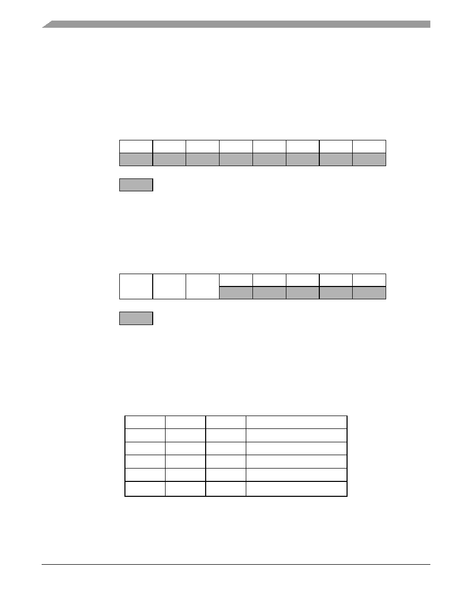
Analog-to-Digital Converter (ADC)
MC68HC908LB8 Data Sheet, Rev. 0
50
Freescale Semiconductor
3.8.2 ADC Data Register
One 8-bit result register is provided. This register is updated each time an ADC conversion completes.
3.8.3 ADC Clock Register
The ADC clock register (ADCLK) selects the clock frequency for the ADC.
ADIV2≠ADIV0 -- ADC Clock Prescaler Bits
ADIV2≠ADIV0 form a 3-bit field which selects the divide ratio used by the ADC to generate the internal
ADC clock.
Table 3-2
shows the available clock configurations. The ADC clock should be set to
approximately 1 MHz.
NOTES:
1. If any unused channels are selected, the resulting ADC conversion will be unknown or re-
served.
2. V
REFH
and V
REFL
are internally connected to V
DD
and V
SS
respectively.
Address:
$003E
Read:
AD7
AD6
AD5
AD4
AD3
AD2
AD1
AD0
Write:
Reset:
Unaffected by reset
= Unimplemented
Figure 3-4. ADC Data Register (ADR)
Address:
$003F
Bit 7
6
5
4
3
2
1
Bit 0
Read:
ADIV2
ADIV1
ADIV0
0
0
0
0
0
Write:
Reset:
0
0
0
0
0
0
0
0
= Unimplemented
Figure 3-5. ADC Clock Register (ADCLK)
Table 3-2. ADC Clock Divide Ratio
ADIV2
ADIV1
ADIV0
ADC Clock Rate
0
0
0
ADC input clock
˜ 1
0
0
1
ADC input clock
˜ 2
0
1
0
ADC input clock
˜ 4
0
1
1
ADC input clock
˜ 8
1
X
(1)
NOTES:
1. X = Don't care
X
(1)
ADC input clock
˜ 16

I/O Registers
MC68HC908LB8 Data Sheet, Rev. 0
Freescale Semiconductor
51
The ADC requires a clock rate of approximately 1 MHz for correct operation. If the selected clock source
is not fast enough, the ADC will generate incorrect conversions. See
20.8 5.0-Volt ADC Characteristics
.
f
ADIC
=
Bus frequency
ADIV[2:0]
1 MHz

Analog-to-Digital Converter (ADC)
MC68HC908LB8 Data Sheet, Rev. 0
52
Freescale Semiconductor

MC68HC908LB8 Data Sheet, Rev. 0
Freescale Semiconductor
53
Chapter 4
Op Amp/Comparator Module
4.1 Introduction
This section describes the functionality of the op amp/comparator.
4.2 Features
Features of the op amp/comparator include:
∑
Software enable/disable
∑
Op amp and comparator modes for optimized performance
∑
Shared output pin with ADC input pin and PWM fault pin to allow a op amp/comparator circuit to
be inputs to these modules
4.3 Pin Name Conventions
The op amp/comparator shares two input pins and an output pin with the port B input/output (I/O). The full
names of the op amp/comparator pins are listed in
Table 4-1
. Note that the generic pin names appear in the text that follows.
Table 4-1. Pin Name Conventions
Generic Pin Name
Full Pin Name
V
OUT
PTB7/V
OUT/
ADC6/FAULT
V≠
PTB6/V≠
V+
PTB5/V+

Op Amp/Comparator Module
MC68HC908LB8 Data Sheet, Rev. 0
54
Freescale Semiconductor
Figure 4-1. Block Diagram Highlighting Op Amp/Comparator Block and Pins
4.4 Functional Description
The op amp/comparator module has two modes of operation -- op amp mode and comparator mode. Op
amp mode optimizes the module for accurate signal amplification with low input offset voltage.
Comparator mode optimizes the module for use as a comparator with fast output response.
The output of the op amp/comparator shares its pin with an analog-to-digital converter (ADC6) channel.
The fault function of the PWM can also be switched to share this pin. The ADC channel function and the
op amp output can be enabled simultaneously so that the output of the op amp could be sampled directly
by the associated ADC channels. See
Figure 4-2.
NOTE
Setting an op amp/comparator enable control bit (OACE) and an op
amp/comparator module selected control bit (OACM) forces V+ and V≠ to
be inputs and V
OUT
to be an output, overriding the data direction register.
M68HC08 CPU
CONTROL AND STATUS
USER FLASH -- 8 KBYTES
USER RAM -- 128 BYTES
MONITOR ROM -- 350 BYTES
USER FLASH VECTOR SPACE -- 34 BYTES
DDRB
PORT
B
DDRC
PORTC
INTERNAL BUS
PTA6
(1)
/AD5/TCH0/KBI6
PTA5
(1)
/RST/KBI5
PTA4
(1)
/AD4/KBI4
PTA3
(1)
/AD3/KBI3
PTA2
(1)
/AD2/KBI2
PTA1
(1)
/AD1/KBI1
PTA0
(1)
/AD0/KBI0
PTB7/V
OUT
/AD6/FAULT
(2)
PTB6/V≠
PTB5/V+
PTB4/PWM1
PTB3/PWM0
PTB2/FAULT
(2)
PTB1/BOT
PTB0/TOP
PTC1
(1)
/OSC2
PTC0
(1)
/OSC1
POWER
V
SS
V
DD
DDRA
PORT
A
PTC2
(1)
/SHTDWN/IRQ
FLASH PROGRAMMING
OSCILLATOR
CPU
REGISTERS
ARITHMETIC/LOGIC
UNIT (ALU)
SYSTEM INTEGRATION
MODULE
DUAL CHANNEL PWM
MODULE
HIGH RESOLUTION PWM
MODULE
LOW-VOLTAGE INHIBIT
MODULE
COMPUTER OPERATING
PROPERLY MODULE
2-CHANNEL TIMER
MODULE
8-BIT ANALOG-TO-DIGITAL
CONVERTER MODULE
OP AMP/COMPARATOR
MODULE
KEYBOARD INTERRUPT
MODULE
MODULE
ROUTINES ROM -- 674 BYTES
REGISTERS -- 64 BYTES
1. Pin contains integrated pullup device.
2. Fault function switchable between pins PTB2 and PTB7.
Notes:

Low Power Modes
MC68HC908LB8 Data Sheet, Rev. 0
Freescale Semiconductor
55
In order to read the digital states of the pins configured as inputs, the data
direction register bit must be a 0; to read the states of the pins configured
as outputs the data direction register bit must be a 1.
Figure 4-2. Op Amp/Comparator Block Diagram
4.5 Low Power Modes
4.5.1 Wait Mode
The WAIT instruction places the MCU in a low power consumption mode. While in WAIT the op
amp/comparator cannot be enabled or disabled. If the op amp/comparator module is not needed during
wait mode, reduce power consumption by disabling the op amp/comparator before executing the WAIT
command.
4.5.2 Stop Mode
The op amp/comparator is inactive after execution of the STOP command. The
op amp/comparator will be in a low-power state and will not drive its output pin. When the MCU exits stop
mode after and external interrupt, the op amp/comparator continues operation.
4.6 Op Amp/Comparator Control Register
There is a single operational control register (OACCR) that contains the enable bit for the op
amp/comparator.
OACM -- Op Amp/Comparator Mode Select Bit
This bit selects between 2 modes of operation, op amp mode and comparator mode.
1 = Op amp mode selected
Address: $0039
Bit 7
6
5
4
3
2
1
Bit 0
Read:
OACM
OACE
Write:
Reset:
0
U
U
U
U
U
U
0
= Unimplemented
U = Unaffected
Figure 4-3. Op Amp/Comparator Control Register (OACCR)
+
-
V
OUT
GROUND
V+
OACE
GROUND
V≠
OACE
OACE
FLOATING
OACE

Op Amp/Comparator Module
MC68HC908LB8 Data Sheet, Rev. 0
56
Freescale Semiconductor
0 = Comparator mode selected
OACE -- Op Amp/Comparator Enable Bit
Setting of the corresponding bit in the register enables the associated op amp/comparator and
connects it to the op amp/comparator pins.
1 = Op amp/comparator is connected to pins and powered on
0 = Op amp/comparator is disconnected from pins and powered off
NOTE
Enabling the op amp/comparator prevents PTB[5:7] from being used as
standard I/O. However, the PTB7 pin can be shared with AD6 and FAULT
if the ADC and PWM modules are also enabled.

MC68HC908LB8 Data Sheet, Rev. 0
Freescale Semiconductor
57
Chapter 5
Configuration Register (CONFIG)
5.1 Introduction
This section describes the configuration registers, CONFIG1 and CONFIG2. The configuration registers
enable or disable these options:
∑
COP timeout period (2
18
≠ 2
4
or 2
13
≠ 2
4
BUSCLKX4 cycles)
∑
STOP instruction
∑
Stop mode recovery (32 x BUSCLKX4 cycles or
4096 x BUSCLKX4 cycles)
∑
Computer operating properly module (COP)
∑
Low-voltage inhibit (LVI) module control
∑
IRQ pin
∑
RST pin
∑
OSC option selection
5.2 Functional Description
The configuration registers are used in the initialization of various options. The configuration registers can
be written once after each reset. All of the configuration register bits are cleared during reset. Since the
various options affect the operation of the microcontroller unit (MCU), it is recommended that these
registers be written immediately after reset. The configuration registers are located at $001E and $001F
and may be read at anytime.
NOTE
On a FLASH device, the options are one-time writable by the user after
each reset. The CONFIG registers are not in the FLASH memory but are
special registers containing one-time writable latches after each reset.
Upon a reset, the CONFIG registers default to predetermined settings as
shown in
Figure 5-1
and
Figure 5-2
.

Configuration Register (CONFIG)
MC68HC908LB8 Data Sheet, Rev. 0
58
Freescale Semiconductor
IRQPUD -- IRQ Pin Pullup Control Bit
1 = Internal pullup is disconnected
0 = Internal pullup is connected between pin IRQ and V
DD
IRQEN -- IRQ Pin Function Selection Bit
1 = Interrupt request function active in pin
0 = Interrupt request function inactive in pin
OSCOPT1 and OSCPOT0 -- Selection Bits for Oscillator Option
RSTEN -- RST Pin Function Selection
1 = Reset function active in pin
0 = Reset function inactive in pin
NOTE
The RSTEN bit is cleared by a power-on reset (POR) only. Other resets will
leave this bit unaffected.
Address:
$001E
Bit 7
6
5
4
3
2
1
Bit 0
Read:
IRQPUD
IRQEN
R
OSCOPT1 OSCOPT0
0
0
RSTEN
Write:
Reset:
0
0
0
0
0
0
0
U
POR:
0
0
0
0
0
0
0
0
= Unimplemented
R
= Reserved
U = Unaffected
Figure 5-1. Configuration Register 2 (CONFIG2)
OSCOPT[1:0]
Oscillator Selection
00
Internal oscillator
01
External oscillator
10
External RC oscillator
11
External XTAL oscillator

Functional Description
MC68HC908LB8 Data Sheet, Rev. 0
Freescale Semiconductor
59
COPRS -- COP Rate Select Bit
COPD selects the COP timeout period. Reset clears COPRS. See
Chapter 6 Computer Operating
Properly (COP) Module
1 = COP timeout period = 2
13
≠ 2
4
BUSCLKX4 cycles
0 = COP timeout period = 2
18
≠ 2
4
BUSCLKX4 cycles
LVISTOP -- LVI Enable in Stop Mode Bit
When the LVIPWRD bit is clear, setting the LVISTOP bit enables the LVI to operate during stop mode.
Reset clears LVISTOP.
1 = LVI enabled during stop mode
0 = LVI disabled during stop mode
LVIRSTD -- LVI Reset Disable Bit
LVIRSTD disables the reset signal from the LVI module. See
Chapter 12 Low-Voltage Inhibit (LVI)
.
1 = LVI module resets disabled
0 = LVI module resets enabled
LVIPWRD -- LVI Power Disable Bit
LVIPWRD disables the LVI module. See
Chapter 12 Low-Voltage Inhibit (LVI)
.
1 = LVI module power disabled
0 = LVI module power enabled
SSREC -- Short Stop Recovery Bit
SSREC enables the CPU to exit stop mode with a delay of 32 BUSCLKX4 cycles instead of a
4096-BUSCLKX4 cycle delay.
1 = Stop mode recovery after 32 BUSCLKX4 cycles
0 = Stop mode recovery after 4096 BUSCLKX4 cycles
NOTE
Exiting stop mode by an LVI reset will result in the long stop recovery.
If running with external crystal, it is advisable to set the short stop recovery bit to 0. The short stop
recovery does not provide enough time for oscillator stabilization and for this reason the SSREC bit
should not be set.
When using the LVI during normal operation but disabling during stop mode, the LVI will have an
enable time of t
EN
. The system stabilization time for power-on reset and long stop recovery (both 4096
BUSCLKX4 cycles) gives a delay longer than the LVI enable time for these startup scenarios. There
is no period where the MCU is not protected from a low-power condition. However, when using the
short stop recovery configuration option, the 32-BUSCLKX4 delay must be greater than the LVI's turn
on time to avoid a period in startup where the LVI is not protecting the MCU.
Address:
$001F
Bit 7
6
5
4
3
2
1
Bit 0
Read:
COPRS
LVISTOP
LVIRSTD
LVIPWRD
0
SSREC
STOP
COPD
Write:
Reset:
0
0
0
0
0
0
0
0
= Unimplemented
Figure 5-2. Configuration Register 1 (CONFIG1)

Configuration Register (CONFIG)
MC68HC908LB8 Data Sheet, Rev. 0
60
Freescale Semiconductor
STOP -- STOP Instruction Enable Bit
STOP enables the STOP instruction.
1 = STOP instruction enabled
0 = STOP instruction treated as illegal opcode
COPD -- COP Disable Bit
COPD disables the COP module. See
Chapter 6 Computer Operating Properly (COP) Module
.
1 = COP module disabled
0 = COP module enabled

MC68HC908LB8 Data Sheet, Rev. 0
Freescale Semiconductor
61
Chapter 6
Computer Operating Properly (COP) Module
6.1 Introduction
The computer operating properly (COP) module contains a free-running counter that generates a reset if
allowed to overflow. The COP module helps software recover from runaway code. Prevent a COP reset
by clearing the COP counter periodically. The COP module can be disabled through the COPD bit in the
configuration 1 (CONFIG1) register.
6.2 Functional Description
Figure 6-1. COP Block Diagram
COPCTL WRITE
BUSCLKX4
RESET VECTOR FETCH
SIM RESET CIRCUIT
RESET STATUS REGISTER
INTERNAL RESET SOURCES
(1)
SIM MODULE
CL
EAR S
T
AGES
5≠12
12-BIT SIM COUNTER
CL
EAR A
LL
STAGES
COPD (FROM CONFIG1)
RESET
COPCTL WRITE
CLEAR
COP MODULE
COPEN (FROM SIM)
COP COUNTER
1. See
Chapter 17 System Integration Module (SIM)
for more details.
COP CLOCK
COP TIMEOUT
COP RATE SELECT
(COPRS FROM CONFIG1)
6-BIT COP COUNTER

Computer Operating Properly (COP) Module
MC68HC908LB8 Data Sheet, Rev. 0
62
Freescale Semiconductor
The COP counter is a free-running 6-bit counter preceded by the 12-bit system integration module (SIM)
counter. If not cleared by software, the COP counter overflows and generates an asynchronous reset after
2
18
≠ 2
4
or 2
13
≠ 2
4
BUSCLKX4 cycles; depending on the state of the COP rate select bit, COPRS, in
configuration register 1. With a 2
18
≠ 2
4
BUSCLKX4 cycle overflow option, using the internal clock to
produce bus speed of 4 MHz gives a COP timeout period of 16.383 ms. Writing any value to location
$FFFF before an overflow occurs prevents a COP reset by clearing the COP counter and stages 12≠5 of
the SIM counter.
NOTE
Service the COP immediately after reset and before entering or after exiting
stop mode to guarantee the maximum time before the first COP counter
overflow.
A COP reset pulls the RST pin low for 32
◊ BUSCLKX4 cycles and sets the COP bit in the reset status
register (RSR). See
17.7.2 SIM Reset Status Register
.
NOTE
Place COP clearing instructions in the main program and not in an interrupt
subroutine. Such an interrupt subroutine could keep the COP from
generating a reset even while the main program is not working properly.
6.3 I/O Signals
The following paragraphs describe the signals shown in
Figure 6-1
.
6.3.1 BUSCLKX4
BUSCLKX4 is the oscillator output signal. BUSCLKX4 frequency is equal to the crystal frequency, the
internal oscillator frequency, or the RC oscillator frequency.
6.3.2 COPCTL Write
Writing any value to the COP control register (COPCTL) (see
6.4 COP Control Register
) clears the COP
counter and clears bits 12≠5 of the SIM counter. Reading the COP control register returns the low byte of
the reset vector.
6.3.3 Power-On Reset
The power-on reset (POR) circuit in the SIM clears the SIM counter 4096
◊ BUSCLKX4 cycles after power
up.
6.3.4 Internal Reset
An internal reset clears the SIM counter and the COP counter.
6.3.5 Reset Vector Fetch
A reset vector fetch occurs when the vector address appears on the data bus. A reset vector fetch clears
the SIM counter.

COP Control Register
MC68HC908LB8 Data Sheet, Rev. 0
Freescale Semiconductor
63
6.3.6 COPD (COP Disable)
The COPD signal reflects the state of the COP disable bit (COPD) in the configuration register 1
(CONFIG1). See
Chapter 5 Configuration Register (CONFIG)
.
6.3.7 COPRS (COP Rate Select)
The COPRS signal reflects the state of the COP rate select bit (COPRS) in the configuration register 1
(CONFIG1). See
Chapter 5 Configuration Register (CONFIG)
.
6.4 COP Control Register
The COP control register (COPCTL) is located at address $FFFF and overlaps the reset vector. Writing
any value to $FFFF clears the COP counter and starts a new timeout period. Reading location $FFFF
returns the low byte of the reset vector.
6.5 Interrupts
The COP does not generate CPU interrupt requests.
6.6 Monitor Mode
The COP is disabled in monitor mode when V
TST
is present on the IRQ pin.
6.7 Low-Power Modes
The WAIT and STOP instructions put the microcontroller unit (MCU) in low power-consumption standby
modes.
6.7.1 Wait Mode
The COP remains active during wait mode. If COP is enabled, a reset will occur at COP timeout.
6.7.2 Stop Mode
Stop mode turns off the BUSCLKX4 input to the COP and clears the SIM counter. Service the COP
immediately before entering or after exiting stop mode to ensure a full COP timeout period after entering
or exiting stop mode.
To prevent inadvertently turning off the COP with a STOP instruction, a configuration option is available
that disables the STOP instruction. When the STOP bit in the configuration register has the STOP
instruction disabled, execution of a STOP instruction results in an illegal opcode reset.
Address: $FFFF
Bit 7
6
5
4
3
2
1
Bit 0
Read:
LOW BYTE OF RESET VECTOR
Write:
CLEAR COP COUNTER
Reset:
Unaffected by reset
Figure 6-2. COP Control Register (COPCTL)

Computer Operating Properly (COP) Module
MC68HC908LB8 Data Sheet, Rev. 0
64
Freescale Semiconductor

MC68HC908LB8 Data Sheet, Rev. 0
Freescale Semiconductor
65
Chapter 7
Central Processor Unit (CPU)
7.1 Introduction
The M68HC08 CPU (central processor unit) is an enhanced and fully object-code-compatible version of
the M68HC05 CPU. The CPU08 Reference Manual (Freescale Semiconductor document order number
CPU08RM/AD) contains a description of the CPU instruction set, addressing modes, and architecture.
7.2 Features
Features of the CPU include:
∑
Object code fully upward-compatible with M68HC05 Family
∑
16-bit stack pointer with stack manipulation instructions
∑
16-bit index register with x-register manipulation instructions
∑
8-MHz CPU internal bus frequency
∑
64-Kbyte program/data memory space
∑
16 addressing modes
∑
Memory-to-memory data moves without using accumulator
∑
Fast 8-bit by 8-bit multiply and 16-bit by 8-bit divide instructions
∑
Enhanced binary-coded decimal (BCD) data handling
∑
Modular architecture with expandable internal bus definition for extension of addressing range
beyond 64 Kbytes
∑
Low-power stop and wait modes
7.3 CPU Registers
Figure 7-1
shows the five CPU registers. CPU registers are not part of the memory map.

Central Processor Unit (CPU)
MC68HC908LB8 Data Sheet, Rev. 0
66
Freescale Semiconductor
Figure 7-1. CPU Registers
7.3.1 Accumulator
The accumulator is a general-purpose 8-bit register. The CPU uses the accumulator to hold operands and
the results of arithmetic/logic operations.
7.3.2 Index Register
The 16-bit index register allows indexed addressing of a 64-Kbyte memory space. H is the upper byte of
the index register, and X is the lower byte. H:X is the concatenated 16-bit index register.
In the indexed addressing modes, the CPU uses the contents of the index register to determine the
conditional address of the operand.
The index register can serve also as a temporary data storage location.
Bit 7
6
5
4
3
2
1
Bit 0
Read:
Write:
Reset:
Unaffected by reset
Figure 7-2. Accumulator (A)
Bit
15
14
13
12
11
10
9
8
7
6
5
4
3
2
1
Bit
0
Read:
Write:
Reset:
0
0
0
0
0
0
0
0
X
X
X
X
X
X
X
X
X = Indeterminate
Figure 7-3. Index Register (H:X)
ACCUMULATOR (A)
INDEX REGISTER (H:X)
STACK POINTER (SP)
PROGRAM COUNTER (PC)
CONDITION CODE REGISTER (CCR)
CARRY/BORROW FLAG
ZERO FLAG
NEGATIVE FLAG
INTERRUPT MASK
HALF-CARRY FLAG
TWO'S COMPLEMENT OVERFLOW FLAG
V 1 1 H
I
N Z C
H
X
0
0
0
0
7
15
15
15
7
0

CPU Registers
MC68HC908LB8 Data Sheet, Rev. 0
Freescale Semiconductor
67
7.3.3 Stack Pointer
The stack pointer is a 16-bit register that contains the address of the next location on the stack. During a
reset, the stack pointer is preset to $00FF. The reset stack pointer (RSP) instruction sets the least
significant byte to $FF and does not affect the most significant byte. The stack pointer decrements as data
is pushed onto the stack and increments as data is pulled from the stack.
In the stack pointer 8-bit offset and 16-bit offset addressing modes, the stack pointer can function as an
index register to access data on the stack. The CPU uses the contents of the stack pointer to determine
the conditional address of the operand.
NOTE
The location of the stack is arbitrary and may be relocated anywhere in
random-access memory (RAM). Moving the SP out of page 0 ($0000 to
$00FF) frees direct address (page 0) space. For correct operation, the
stack pointer must point only to RAM locations.
7.3.4 Program Counter
The program counter is a 16-bit register that contains the address of the next instruction or operand to be
fetched.
Normally, the program counter automatically increments to the next sequential memory location every
time an instruction or operand is fetched. Jump, branch, and interrupt operations load the program
counter with an address other than that of the next sequential location.
During reset, the program counter is loaded with the reset vector address located at $FFFE and $FFFF.
The vector address is the address of the first instruction to be executed after exiting the reset state.
7.3.5 Condition Code Register
The 8-bit condition code register contains the interrupt mask and five flags that indicate the results of the
instruction just executed. Bits 6 and 5 are set permanently to 1. The following paragraphs describe the
functions of the condition code register.
Bit
15
14
13
12
11
10
9
8
7
6
5
4
3
2
1
Bit
0
Read:
Write:
Reset:
0
0
0
0
0
0
0
0
1
1
1
1
1
1
1
1
Figure 7-4. Stack Pointer (SP)
Bit
15
14
13
12
11
10
9
8
7
6
5
4
3
2
1
Bit
0
Read:
Write:
Reset:
Loaded with vector from $FFFE and $FFFF
Figure 7-5. Program Counter (PC)

Central Processor Unit (CPU)
MC68HC908LB8 Data Sheet, Rev. 0
68
Freescale Semiconductor
V -- Overflow Flag
The CPU sets the overflow flag when a two's complement overflow occurs. The signed branch
instructions BGT, BGE, BLE, and BLT use the overflow flag.
1 = Overflow
0 = No overflow
H -- Half-Carry Flag
The CPU sets the half-carry flag when a carry occurs between accumulator bits 3 and 4 during an
add-without-carry (ADD) or add-with-carry (ADC) operation. The half-carry flag is required for
binary-coded decimal (BCD) arithmetic operations. The DAA instruction uses the states of the H and
C flags to determine the appropriate correction factor.
1 = Carry between bits 3 and 4
0 = No carry between bits 3 and 4
I -- Interrupt Mask
When the interrupt mask is set, all maskable CPU interrupts are disabled. CPU interrupts are enabled
when the interrupt mask is cleared. When a CPU interrupt occurs, the interrupt mask is set
automatically after the CPU registers are saved on the stack, but before the interrupt vector is fetched.
1 = Interrupts disabled
0 = Interrupts enabled
NOTE
To maintain M6805 Family compatibility, the upper byte of the index
register (H) is not stacked automatically. If the interrupt service routine
modifies H, then the user must stack and unstack H using the PSHH and
PULH instructions.
After the I bit is cleared, the highest-priority interrupt request is serviced first.
A return-from-interrupt (RTI) instruction pulls the CPU registers from the stack and restores the
interrupt mask from the stack. After any reset, the interrupt mask is set and can be cleared only by the
clear interrupt mask software instruction (CLI).
N -- Negative flag
The CPU sets the negative flag when an arithmetic operation, logic operation, or data manipulation
produces a negative result, setting bit 7 of the result.
1 = Negative result
0 = Non-negative result
Z -- Zero flag
The CPU sets the zero flag when an arithmetic operation, logic operation, or data manipulation
produces a result of $00.
1 = Zero result
0 = Non-zero result
Bit 7
6
5
4
3
2
1
Bit 0
Read:
V
1
1
H
I
N
Z
C
Write:
Reset:
X
1
1
X
1
X
X
X
X = Indeterminate
Figure 7-6. Condition Code Register (CCR)

Arithmetic/Logic Unit (ALU)
MC68HC908LB8 Data Sheet, Rev. 0
Freescale Semiconductor
69
C -- Carry/Borrow Flag
The CPU sets the carry/borrow flag when an addition operation produces a carry out of bit 7 of the
accumulator or when a subtraction operation requires a borrow. Some instructions -- such as bit test
and branch, shift, and rotate -- also clear or set the carry/borrow flag.
1 = Carry out of bit 7
0 = No carry out of bit 7
7.4 Arithmetic/Logic Unit (ALU)
The ALU performs the arithmetic and logic operations defined by the instruction set.
Refer to the CPU08 Reference Manual (Freescale Semiconductor document order number
CPU08RM/AD) for a description of the instructions and addressing modes and more detail about the
architecture of the CPU.
7.5 Low-Power Modes
The WAIT and STOP instructions put the MCU in low power-consumption standby modes.
7.5.1 Wait Mode
The WAIT instruction:
∑
Clears the interrupt mask (I bit) in the condition code register, enabling interrupts. After exit from
wait mode by interrupt, the I bit remains clear. After exit by reset, the I bit is set.
∑
Disables the CPU clock
7.5.2 Stop Mode
The STOP instruction:
∑
Clears the interrupt mask (I bit) in the condition code register, enabling external interrupts. After
exit from stop mode by external interrupt, the I bit remains clear. After exit by reset, the I bit is set.
∑
Disables the CPU clock
After exiting stop mode, the CPU clock begins running after the oscillator stabilization delay.
7.6 CPU During Break Interrupts
If a break module is present on the MCU, the CPU starts a break interrupt by:
∑
Loading the instruction register with the SWI instruction
∑
Loading the program counter with $FFFC:$FFFD or with $FEFC:$FEFD in monitor mode
The break interrupt begins after completion of the CPU instruction in progress. If the break address
register match occurs on the last cycle of a CPU instruction, the break interrupt begins immediately.
A return-from-interrupt instruction (RTI) in the break routine ends the break interrupt and returns the MCU
to normal operation if the break interrupt has been deasserted.

Central Processor Unit (CPU)
MC68HC908LB8 Data Sheet, Rev. 0
70
Freescale Semiconductor
7.7 Instruction Set Summary
Table 7-1
provides a summary of the M68HC08 instruction set.
Table 7-1. Instruction Set Summary (Sheet 1 of 7)
Source
Form
Operation
Description
Effect
on CCR
Add
r
es
s
Mode
Opc
ode
Ope
r
and
Cy
cl
es
V H I N Z C
ADC #opr
ADC opr
ADC opr
ADC opr,X
ADC opr,X
ADC ,X
ADC opr,SP
ADC opr,SP
Add with Carry
A
(A) + (M) + (C)
≠
IMM
DIR
EXT
IX2
IX1
IX
SP1
SP2
A9
B9
C9
D9
E9
F9
9EE9
9ED9
ii
dd
hh ll
ee ff
ff
ff
ee ff
2
3
4
4
3
2
4
5
ADD #opr
ADD opr
ADD opr
ADD opr,X
ADD opr,X
ADD ,X
ADD opr,SP
ADD opr,SP
Add without Carry
A
(A) + (M)
≠
IMM
DIR
EXT
IX2
IX1
IX
SP1
SP2
AB
BB
CB
DB
EB
FB
9EEB
9EDB
ii
dd
hh ll
ee ff
ff
ff
ee ff
2
3
4
4
3
2
4
5
AIS #opr
Add Immediate Value (Signed) to SP
SP
(SP) + (16
´
M)
≠ ≠ ≠ ≠ ≠ ≠ IMM
A7
ii 2
AIX #opr
Add Immediate Value (Signed) to H:X
H:X
(H:X) + (16
´
M)
≠ ≠ ≠ ≠ ≠ ≠ IMM
AF
ii
2
AND #opr
AND opr
AND opr
AND opr,X
AND opr,X
AND ,X
AND opr,SP
AND opr,SP
Logical AND
A
(A) & (M)
0 ≠ ≠
≠
IMM
DIR
EXT
IX2
IX1
IX
SP1
SP2
A4
B4
C4
D4
E4
F4
9EE4
9ED4
ii
dd
hh ll
ee ff
ff
ff
ee ff
2
3
4
4
3
2
4
5
ASL opr
ASLA
ASLX
ASL opr,X
ASL ,X
ASL opr,SP
Arithmetic Shift Left
(Same as LSL)
≠ ≠
DIR
INH
INH
IX1
IX
SP1
38
48
58
68
78
9E68
dd
ff
ff
4
1
1
4
3
5
ASR opr
ASRA
ASRX
ASR opr,X
ASR opr,X
ASR opr,SP
Arithmetic Shift Right
≠ ≠
DIR
INH
INH
IX1
IX
SP1
37
47
57
67
77
9E67
dd
ff
ff
4
1
1
4
3
5
BCC rel
Branch if Carry Bit Clear
PC
(PC) + 2 + rel ? (C) = 0
≠ ≠ ≠ ≠ ≠ ≠ REL
24
rr
3
BCLR n, opr
Clear Bit n in M
Mn
0
≠ ≠ ≠ ≠ ≠ ≠
DIR (b0)
DIR (b1)
DIR (b2)
DIR (b3)
DIR (b4)
DIR (b5)
DIR (b6)
DIR (b7)
11
13
15
17
19
1B
1D
1F
dd
dd
dd
dd
dd
dd
dd
dd
4
4
4
4
4
4
4
4
BCS rel
Branch if Carry Bit Set (Same as BLO)
PC
(PC) + 2 + rel ? (C) = 1
≠ ≠ ≠ ≠ ≠ ≠ REL
25
rr
3
BEQ rel
Branch if Equal
PC
(PC) + 2 + rel ? (Z) = 1
≠ ≠ ≠ ≠ ≠ ≠ REL
27
rr
3
BGE opr
Branch if Greater Than or Equal To
(Signed Operands)
PC
(PC) + 2 + rel ? (N
V
) = 0
≠ ≠ ≠ ≠ ≠ ≠ REL
90
rr
3
C
b0
b7
0
b0
b7
C

Instruction Set Summary
MC68HC908LB8 Data Sheet, Rev. 0
Freescale Semiconductor
71
BGT opr
Branch if Greater Than (Signed
Operands)
PC
(PC) + 2 + rel ? (Z) | (N
V
) = 0 ≠ ≠ ≠ ≠ ≠ ≠ REL
92
rr
3
BHCC rel
Branch if Half Carry Bit Clear
PC
(PC) + 2 + rel ? (H) = 0
≠ ≠ ≠ ≠ ≠ ≠ REL
28
rr
3
BHCS rel
Branch if Half Carry Bit Set
PC
(PC) + 2 + rel ? (H) = 1
≠ ≠ ≠ ≠ ≠ ≠ REL
29
rr
3
BHI rel
Branch if Higher
PC
(PC) + 2 + rel ? (C) | (Z) = 0
≠ ≠ ≠ ≠ ≠ ≠ REL
22
rr
3
BHS rel
Branch if Higher or Same
(Same as BCC)
PC
(PC) + 2 + rel ? (C) = 0
≠ ≠ ≠ ≠ ≠ ≠ REL
24
rr
3
BIH rel
Branch if IRQ Pin High
PC
(PC) + 2 + rel ? IRQ = 1
≠ ≠ ≠ ≠ ≠ ≠ REL
2F
rr
3
BIL rel
Branch if IRQ Pin Low
PC
(PC) + 2 + rel ? IRQ = 0
≠ ≠ ≠ ≠ ≠ ≠ REL
2E
rr
3
BIT #opr
BIT opr
BIT opr
BIT opr,X
BIT opr,X
BIT ,X
BIT opr,SP
BIT opr,SP
Bit Test
(A) & (M)
0 ≠ ≠
≠
IMM
DIR
EXT
IX2
IX1
IX
SP1
SP2
A5
B5
C5
D5
E5
F5
9EE5
9ED5
ii
dd
hh ll
ee ff
ff
ff
ee ff
2
3
4
4
3
2
4
5
BLE opr
Branch if Less Than or Equal To
(Signed Operands)
PC
(PC) + 2 + rel ? (Z) | (N
V) = 1 ≠ ≠ ≠ ≠ ≠ ≠ REL
93
rr
3
BLO rel
Branch if Lower (Same as BCS)
PC
(PC) + 2 + rel ? (C) = 1
≠ ≠ ≠ ≠ ≠ ≠ REL
25
rr
3
BLS rel
Branch if Lower or Same
PC
(PC) + 2 + rel ? (C) | (Z) = 1
≠ ≠ ≠ ≠ ≠ ≠ REL
23
rr
3
BLT opr
Branch if Less Than (Signed Operands)
PC
(PC) + 2 + rel ? (N
V
) =1
≠ ≠ ≠ ≠ ≠ ≠ REL
91
rr
3
BMC rel
Branch if Interrupt Mask Clear
PC
(PC) + 2 + rel ? (I) = 0
≠ ≠ ≠ ≠ ≠ ≠ REL
2C
rr
3
BMI rel
Branch if Minus
PC
(PC) + 2 + rel ? (N) = 1
≠ ≠ ≠ ≠ ≠ ≠ REL
2B
rr
3
BMS rel
Branch if Interrupt Mask Set
PC
(PC) + 2 + rel ? (I) = 1
≠ ≠ ≠ ≠ ≠ ≠ REL
2D
rr
3
BNE rel
Branch if Not Equal
PC
(PC) + 2 + rel ? (Z) = 0
≠ ≠ ≠ ≠ ≠ ≠ REL
26
rr
3
BPL rel
Branch if Plus
PC
(PC) + 2 + rel ? (N) = 0
≠ ≠ ≠ ≠ ≠ ≠ REL
2A
rr
3
BRA rel
Branch Always
PC
(PC) + 2 + rel ≠ ≠ ≠ ≠ ≠ ≠ REL
20
rr
3
BRCLR n,opr,rel Branch if Bit n in M Clear
PC
(PC) + 3 + rel ? (Mn) = 0
≠ ≠ ≠ ≠ ≠
DIR (b0)
DIR (b1)
DIR (b2)
DIR (b3)
DIR (b4)
DIR (b5)
DIR (b6)
DIR (b7)
01
03
05
07
09
0B
0D
0F
dd rr
dd rr
dd rr
dd rr
dd rr
dd rr
dd rr
dd rr
5
5
5
5
5
5
5
5
BRN rel
Branch Never
PC
(PC) + 2
≠ ≠ ≠ ≠ ≠ ≠ REL
21
rr
3
BRSET n,opr,rel Branch if Bit n in M Set
PC
(PC) + 3 + rel ? (Mn) = 1
≠ ≠ ≠ ≠ ≠
DIR (b0)
DIR (b1)
DIR (b2)
DIR (b3)
DIR (b4)
DIR (b5)
DIR (b6)
DIR (b7)
00
02
04
06
08
0A
0C
0E
dd rr
dd rr
dd rr
dd rr
dd rr
dd rr
dd rr
dd rr
5
5
5
5
5
5
5
5
Table 7-1. Instruction Set Summary (Sheet 2 of 7)
Source
Form
Operation
Description
Effect
on CCR
Address
M
ode
Opc
o
de
O
p
er
and
Cy
cl
es
V H I N Z C

Central Processor Unit (CPU)
MC68HC908LB8 Data Sheet, Rev. 0
72
Freescale Semiconductor
BSET n,opr
Set Bit n in M
Mn
1
≠ ≠ ≠ ≠ ≠ ≠
DIR (b0)
DIR (b1)
DIR (b2)
DIR (b3)
DIR (b4)
DIR (b5)
DIR (b6)
DIR (b7)
10
12
14
16
18
1A
1C
1E
dd
dd
dd
dd
dd
dd
dd
dd
4
4
4
4
4
4
4
4
BSR rel
Branch to Subroutine
PC
(PC) + 2; push (PCL)
SP
(SP) ≠ 1; push (PCH)
SP
(SP) ≠ 1
PC
(PC) + rel
≠ ≠ ≠ ≠ ≠ ≠ REL
AD
rr
4
CBEQ opr,rel
CBEQA #opr,rel
CBEQX #opr,rel
CBEQ opr,X+,rel
CBEQ X+,rel
CBEQ opr,SP,rel
Compare and Branch if Equal
PC
(PC) + 3 + rel ? (A) ≠ (M) = $00
PC
(PC) + 3 + rel ? (A) ≠ (M) = $00
PC
(PC) + 3 + rel ? (X) ≠ (M) = $00
PC
(PC) + 3 + rel ? (A) ≠ (M) = $00
PC
(PC) + 2 + rel ? (A) ≠ (M) = $00
PC
(PC) + 4 + rel ? (A) ≠ (M) = $00
≠ ≠ ≠ ≠ ≠ ≠
DIR
IMM
IMM
IX1+
IX+
SP1
31
41
51
61
71
9E61
dd rr
ii rr
ii rr
ff rr
rr
ff rr
5
4
4
5
4
6
CLC
Clear Carry Bit
C
0
≠ ≠ ≠ ≠ ≠ 0 INH
98
1
CLI
Clear Interrupt Mask
I
0
≠ ≠ 0 ≠ ≠ ≠ INH
9A
2
CLR opr
CLRA
CLRX
CLRH
CLR opr,X
CLR ,X
CLR opr,SP
Clear
M
$00
A
$00
X
$00
H
$00
M
$00
M
$00
M
$00
0 ≠ ≠ 0 1 ≠
DIR
INH
INH
INH
IX1
IX
SP1
3F
4F
5F
8C
6F
7F
9E6F
dd
ff
ff
3
1
1
1
3
2
4
CMP #opr
CMP opr
CMP opr
CMP opr,X
CMP opr,X
CMP ,X
CMP opr,SP
CMP opr,SP
Compare A with M
(A) ≠ (M)
≠ ≠
IMM
DIR
EXT
IX2
IX1
IX
SP1
SP2
A1
B1
C1
D1
E1
F1
9EE1
9ED1
ii
dd
hh ll
ee ff
ff
ff
ee ff
2
3
4
4
3
2
4
5
COM opr
COMA
COMX
COM opr,X
COM ,X
COM opr,SP
Complement (One's Complement)
M
(M) = $FF ≠ (M)
A
(A) = $FF ≠ (M)
X
(X) = $FF ≠ (M)
M
(M) = $FF ≠ (M)
M
(M) = $FF ≠ (M)
M
(M) = $FF ≠ (M)
0 ≠ ≠
1
DIR
INH
INH
IX1
IX
SP1
33
43
53
63
73
9E63
dd
ff
ff
4
1
1
4
3
5
CPHX #opr
CPHX opr
Compare H:X with M
(H:X) ≠ (M:M + 1)
≠ ≠
IMM
DIR
65
75
ii ii+1
dd
3
4
CPX #opr
CPX opr
CPX opr
CPX ,X
CPX opr,X
CPX opr,X
CPX opr,SP
CPX opr,SP
Compare X with M
(X) ≠ (M)
≠ ≠
IMM
DIR
EXT
IX2
IX1
IX
SP1
SP2
A3
B3
C3
D3
E3
F3
9EE3
9ED3
ii
dd
hh ll
ee ff
ff
ff
ee ff
2
3
4
4
3
2
4
5
DAA
Decimal Adjust A
(A)
10
U ≠ ≠
INH
72
2
DBNZ opr,rel
DBNZA rel
DBNZX rel
DBNZ opr,X,rel
DBNZ X,rel
DBNZ opr,SP,rel
Decrement and Branch if Not Zero
A
(A) ≠ 1 or M (M) ≠ 1 or X (X) ≠ 1
PC
(PC) + 3 + rel ? (result) 0
PC
(PC) + 2 + rel ? (result) 0
PC
(PC) + 2 + rel ? (result) 0
PC
(PC) + 3 + rel ? (result) 0
PC
(PC) + 2 + rel ? (result) 0
PC
(PC) + 4 + rel ? (result) 0
≠ ≠ ≠ ≠ ≠ ≠
DIR
INH
INH
IX1
IX
SP1
3B
4B
5B
6B
7B
9E6B
dd rr
rr
rr
ff rr
rr
ff rr
5
3
3
5
4
6
Table 7-1. Instruction Set Summary (Sheet 3 of 7)
Source
Form
Operation
Description
Effect
on CCR
Address
M
ode
Opc
o
de
O
p
er
and
Cy
cl
es
V H I N Z C

Instruction Set Summary
MC68HC908LB8 Data Sheet, Rev. 0
Freescale Semiconductor
73
DEC opr
DECA
DECX
DEC opr,X
DEC ,X
DEC opr,SP
Decrement
M
(M) ≠ 1
A
(A) ≠ 1
X
(X) ≠ 1
M
(M) ≠ 1
M
(M) ≠ 1
M
(M) ≠ 1
≠ ≠
≠
DIR
INH
INH
IX1
IX
SP1
3A
4A
5A
6A
7A
9E6A
dd
ff
ff
4
1
1
4
3
5
DIV
Divide
A
(H:A)/(X)
H
Remainder
≠ ≠ ≠ ≠
INH
52
7
EOR #opr
EOR opr
EOR opr
EOR opr,X
EOR opr,X
EOR ,X
EOR opr,SP
EOR opr,SP
Exclusive OR M with A
A
(A
M)
0 ≠ ≠
≠
IMM
DIR
EXT
IX2
IX1
IX
SP1
SP2
A8
B8
C8
D8
E8
F8
9EE8
9ED8
ii
dd
hh ll
ee ff
ff
ff
ee ff
2
3
4
4
3
2
4
5
INC opr
INCA
INCX
INC opr,X
INC ,X
INC opr,SP
Increment
M
(M) + 1
A
(A) + 1
X
(X) + 1
M
(M) + 1
M
(M) + 1
M
(M) + 1
≠ ≠
≠
DIR
INH
INH
IX1
IX
SP1
3C
4C
5C
6C
7C
9E6C
dd
ff
ff
4
1
1
4
3
5
JMP opr
JMP opr
JMP opr,X
JMP opr,X
JMP ,X
Jump
PC
Jump Address
≠ ≠ ≠ ≠ ≠ ≠
DIR
EXT
IX2
IX1
IX
BC
CC
DC
EC
FC
dd
hh ll
ee ff
ff
2
3
4
3
2
JSR opr
JSR opr
JSR opr,X
JSR opr,X
JSR ,X
Jump to Subroutine
PC
(PC) + n (n = 1, 2, or 3)
Push (PCL); SP
(SP) ≠ 1
Push (PCH); SP
(SP) ≠ 1
PC
Unconditional Address
≠ ≠ ≠ ≠ ≠ ≠
DIR
EXT
IX2
IX1
IX
BD
CD
DD
ED
FD
dd
hh ll
ee ff
ff
4
5
6
5
4
LDA #opr
LDA opr
LDA opr
LDA opr,X
LDA opr,X
LDA ,X
LDA opr,SP
LDA opr,SP
Load A from M
A
(M)
0 ≠ ≠
≠
IMM
DIR
EXT
IX2
IX1
IX
SP1
SP2
A6
B6
C6
D6
E6
F6
9EE6
9ED6
ii
dd
hh ll
ee ff
ff
ff
ee ff
2
3
4
4
3
2
4
5
LDHX #opr
LDHX opr
Load H:X from M
H:X
(M:M + 1)
0 ≠ ≠
≠
IMM
DIR
45
55
ii jj
dd
3
4
LDX #opr
LDX opr
LDX opr
LDX opr,X
LDX opr,X
LDX ,X
LDX opr,SP
LDX opr,SP
Load X from M
X
(M)
0 ≠ ≠
≠
IMM
DIR
EXT
IX2
IX1
IX
SP1
SP2
AE
BE
CE
DE
EE
FE
9EEE
9EDE
ii
dd
hh ll
ee ff
ff
ff
ee ff
2
3
4
4
3
2
4
5
LSL opr
LSLA
LSLX
LSL opr,X
LSL ,X
LSL opr,SP
Logical Shift Left
(Same as ASL)
≠ ≠
DIR
INH
INH
IX1
IX
SP1
38
48
58
68
78
9E68
dd
ff
ff
4
1
1
4
3
5
Table 7-1. Instruction Set Summary (Sheet 4 of 7)
Source
Form
Operation
Description
Effect
on CCR
Address
M
ode
Opc
o
de
O
p
er
and
Cy
cl
es
V H I N Z C
C
b0
b7
0

Central Processor Unit (CPU)
MC68HC908LB8 Data Sheet, Rev. 0
74
Freescale Semiconductor
LSR opr
LSRA
LSRX
LSR opr,X
LSR ,X
LSR opr,SP
Logical Shift Right
≠ ≠ 0
DIR
INH
INH
IX1
IX
SP1
34
44
54
64
74
9E64
dd
ff
ff
4
1
1
4
3
5
MOV opr,opr
MOV opr,X+
MOV #opr,opr
MOV X+,opr
Move
(M)
Destination
(M)
Source
H:X
(H:X) + 1 (IX+D, DIX+)
0 ≠ ≠
≠
DD
DIX+
IMD
IX+D
4E
5E
6E
7E
dd dd
dd
ii dd
dd
5
4
4
4
MUL
Unsigned multiply
X:A
(X) ◊ (A)
≠ 0 ≠ ≠ ≠ 0 INH
42
5
NEG opr
NEGA
NEGX
NEG opr,X
NEG ,X
NEG opr,SP
Negate (Two's Complement)
M
≠(M) = $00 ≠ (M)
A
≠(A) = $00 ≠ (A)
X
≠(X) = $00 ≠ (X)
M
≠(M) = $00 ≠ (M)
M
≠(M) = $00 ≠ (M)
≠ ≠
DIR
INH
INH
IX1
IX
SP1
30
40
50
60
70
9E60
dd
ff
ff
4
1
1
4
3
5
NOP
No Operation
None
≠ ≠ ≠ ≠ ≠ ≠ INH
9D
1
NSA
Nibble Swap A
A
(A[3:0]:A[7:4])
≠ ≠ ≠ ≠ ≠ ≠ INH
62
3
ORA #opr
ORA opr
ORA opr
ORA opr,X
ORA opr,X
ORA ,X
ORA opr,SP
ORA opr,SP
Inclusive OR A and M
A
(A) | (M)
0 ≠ ≠
≠
IMM
DIR
EXT
IX2
IX1
IX
SP1
SP2
AA
BA
CA
DA
EA
FA
9EEA
9EDA
ii
dd
hh ll
ee ff
ff
ff
ee ff
2
3
4
4
3
2
4
5
PSHA
Push A onto Stack
Push (A); SP
(SP) ≠ 1
≠ ≠ ≠ ≠ ≠ ≠ INH
87
2
PSHH
Push H onto Stack
Push (H); SP
(SP) ≠ 1
≠ ≠ ≠ ≠ ≠ ≠ INH
8B
2
PSHX
Push X onto Stack
Push (X); SP
(SP) ≠ 1
≠ ≠ ≠ ≠ ≠ ≠ INH
89
2
PULA
Pull A from Stack
SP
(SP + 1); Pull (A)
≠ ≠ ≠ ≠ ≠ ≠ INH
86
2
PULH
Pull H from Stack
SP
(SP + 1); Pull (H)
≠ ≠ ≠ ≠ ≠ ≠ INH
8A
2
PULX
Pull X from Stack
SP
(SP + 1); Pull (X)
≠ ≠ ≠ ≠ ≠ ≠ INH
88
2
ROL opr
ROLA
ROLX
ROL opr,X
ROL ,X
ROL opr,SP
Rotate Left through Carry
≠ ≠
DIR
INH
INH
IX1
IX
SP1
39
49
59
69
79
9E69
dd
ff
ff
4
1
1
4
3
5
ROR opr
RORA
RORX
ROR opr,X
ROR ,X
ROR opr,SP
Rotate Right through Carry
≠ ≠
DIR
INH
INH
IX1
IX
SP1
36
46
56
66
76
9E66
dd
ff
ff
4
1
1
4
3
5
RSP
Reset Stack Pointer
SP
$FF
≠ ≠ ≠ ≠ ≠ ≠ INH
9C
1
RTI
Return from Interrupt
SP
(SP) + 1; Pull (CCR)
SP
(SP) + 1; Pull (A)
SP
(SP) + 1; Pull (X)
SP
(SP) + 1; Pull (PCH)
SP
(SP) + 1; Pull (PCL)
INH
80
7
RTS
Return from Subroutine
SP
SP + 1; Pull (PCH)
SP
SP + 1; Pull (PCL)
≠ ≠ ≠ ≠ ≠ ≠ INH
81
4
Table 7-1. Instruction Set Summary (Sheet 5 of 7)
Source
Form
Operation
Description
Effect
on CCR
Address
M
ode
Opc
o
de
O
p
er
and
Cy
cl
es
V H I N Z C
b0
b7
C
0
C
b0
b7
b0
b7
C

Instruction Set Summary
MC68HC908LB8 Data Sheet, Rev. 0
Freescale Semiconductor
75
SBC #opr
SBC opr
SBC opr
SBC opr,X
SBC opr,X
SBC ,X
SBC opr,SP
SBC opr,SP
Subtract with Carry
A
(A) ≠ (M) ≠ (C)
≠ ≠
IMM
DIR
EXT
IX2
IX1
IX
SP1
SP2
A2
B2
C2
D2
E2
F2
9EE2
9ED2
ii
dd
hh ll
ee ff
ff
ff
ee ff
2
3
4
4
3
2
4
5
SEC
Set Carry Bit
C
1
≠ ≠ ≠ ≠ ≠ 1 INH
99
1
SEI
Set Interrupt Mask
I
1
≠ ≠ 1 ≠ ≠ ≠ INH
9B
2
STA opr
STA opr
STA opr,X
STA opr,X
STA ,X
STA opr,SP
STA opr,SP
Store A in M
M
(A)
0 ≠ ≠
≠
DIR
EXT
IX2
IX1
IX
SP1
SP2
B7
C7
D7
E7
F7
9EE7
9ED7
dd
hh ll
ee ff
ff
ff
ee ff
3
4
4
3
2
4
5
STHX opr
Store H:X in M
(M:M + 1)
(H:X)
0 ≠ ≠
≠ DIR
35
dd
4
STOP
Enable Interrupts, Stop Processing,
Refer to MCU Documentation
I
0; Stop Processing
≠ ≠ 0 ≠ ≠ ≠ INH
8E
1
STX opr
STX opr
STX opr,X
STX opr,X
STX ,X
STX opr,SP
STX opr,SP
Store X in M
M
(X)
0 ≠ ≠
≠
DIR
EXT
IX2
IX1
IX
SP1
SP2
BF
CF
DF
EF
FF
9EEF
9EDF
dd
hh ll
ee ff
ff
ff
ee ff
3
4
4
3
2
4
5
SUB #opr
SUB opr
SUB opr
SUB opr,X
SUB opr,X
SUB ,X
SUB opr,SP
SUB opr,SP
Subtract A
(A) ≠ (M)
≠ ≠
IMM
DIR
EXT
IX2
IX1
IX
SP1
SP2
A0
B0
C0
D0
E0
F0
9EE0
9ED0
ii
dd
hh ll
ee ff
ff
ff
ee ff
2
3
4
4
3
2
4
5
SWI
Software Interrupt
PC
(PC) + 1; Push (PCL)
SP
(SP) ≠ 1; Push (PCH)
SP
(SP) ≠ 1; Push (X)
SP
(SP) ≠ 1; Push (A)
SP
(SP) ≠ 1; Push (CCR)
SP
(SP) ≠ 1; I 1
PCH
Interrupt Vector High Byte
PCL
Interrupt Vector Low Byte
≠ ≠ 1 ≠ ≠ ≠ INH
83
9
TAP
Transfer A to CCR
CCR
(A)
INH
84
2
TAX
Transfer A to X
X
(A)
≠ ≠ ≠ ≠ ≠ ≠ INH
97
1
TPA
Transfer CCR to A
A
(CCR)
≠ ≠ ≠ ≠ ≠ ≠ INH
85
1
TST opr
TSTA
TSTX
TST opr,X
TST ,X
TST opr,SP
Test for Negative or Zero
(A) ≠ $00 or (X) ≠ $00 or (M) ≠ $00
0 ≠ ≠
≠
DIR
INH
INH
IX1
IX
SP1
3D
4D
5D
6D
7D
9E6D
dd
ff
ff
3
1
1
3
2
4
TSX
Transfer SP to H:X
H:X
(SP) + 1
≠ ≠ ≠ ≠ ≠ ≠ INH
95
2
TXA
Transfer X to A
A
(X)
≠ ≠ ≠ ≠ ≠ ≠ INH
9F
1
TXS
Transfer H:X to SP
(SP)
(H:X) ≠ 1
≠ ≠ ≠ ≠ ≠ ≠ INH
94
2
Table 7-1. Instruction Set Summary (Sheet 6 of 7)
Source
Form
Operation
Description
Effect
on CCR
Address
M
ode
Opc
o
de
O
p
er
and
Cy
cl
es
V H I N Z C

Central Processor Unit (CPU)
MC68HC908LB8 Data Sheet, Rev. 0
76
Freescale Semiconductor
7.8 Opcode Map
See
Table 7-2
.
WAIT
Enable Interrupts; Wait for Interrupt
I bit
0; Inhibit CPU clocking
until interrupted
≠ ≠ 0 ≠ ≠ ≠ INH
8F
1
A
Accumulator
n
Any bit
C
Carry/borrow bit
opr
Operand (one or two bytes)
CCR
Condition code register
PC
Program counter
dd
Direct address of operand
PCH Program counter high byte
dd rr
Direct address of operand and relative offset of branch instruction
PCL Program counter low byte
DD
Direct to direct addressing mode
REL Relative addressing mode
DIR
Direct addressing mode
rel
Relative program counter offset byte
DIX+
Direct to indexed with post increment addressing mode
rr
Relative program counter offset byte
ee ff
High and low bytes of offset in indexed, 16-bit offset addressing
SP1 Stack pointer, 8-bit offset addressing mode
EXT
Extended addressing mode
SP2 Stack pointer 16-bit offset addressing mode
ff
Offset byte in indexed, 8-bit offset addressing
SP
Stack pointer
H
Half-carry bit
U
Undefined
H
Index register high byte
V
Overflow bit
hh ll
High and low bytes of operand address in extended addressing
X
Index register low byte
I
Interrupt mask
Z
Zero bit
ii
Immediate operand byte
&
Logical AND
IMD
Immediate source to direct destination addressing mode
|
Logical OR
IMM
Immediate addressing mode
Logical EXCLUSIVE OR
INH
Inherent addressing mode
( )
Contents of
IX
Indexed, no offset addressing mode
≠( )
Negation (two's complement)
IX+
Indexed, no offset, post increment addressing mode
#
Immediate value
IX+D
Indexed with post increment to direct addressing mode
´
Sign extend
IX1
Indexed, 8-bit offset addressing mode
Loaded with
IX1+
Indexed, 8-bit offset, post increment addressing mode
?
If
IX2
Indexed, 16-bit offset addressing mode
:
Concatenated with
M
Memory location
Set or cleared
N
Negative bit
--
Not affected
Table 7-1. Instruction Set Summary (Sheet 7 of 7)
Source
Form
Operation
Description
Effect
on CCR
Address
M
ode
Opc
o
de
O
p
er
and
Cy
cl
es
V H I N Z C

Table 7-2. Opcode Map
Bit Manipulation
Branch
Read-Modify-Write
Control
Register/Memory
DIR
DIR
REL
DIR
INH
INH
IX1
SP1
IX
INH
INH
IMM
DIR
EXT
IX2
SP2
IX1
SP1
IX
0
1
2
3
4
5
6
9E6
7
8
9
A
B
C
D
9ED
E
9EE
F
0
5
BRSET0
3
DIR
4
BSET0
2
DIR
3
BRA
2
REL
4
NEG
2
DIR
1
NEGA
1
INH
1
NEGX
1
INH
4
NEG
2
IX1
5
NEG
3
SP1
3
NEG
1
IX
7
RTI
1
INH
3
BGE
2
REL
2
SUB
2
IMM
3
SUB
2
DIR
4
SUB
3
EXT
4
SUB
3
IX2
5
SUB
4
SP2
3
SUB
2
IX1
4
SUB
3
SP1
2
SUB
1
IX
1
5
BRCLR0
3
DIR
4
BCLR0
2
DIR
3
BRN
2
REL
5
CBEQ
3
DIR
4
CBEQA
3
IMM
4
CBEQX
3
IMM
5
CBEQ
3 IX1+
6
CBEQ
4
SP1
4
CBEQ
2
IX+
4
RTS
1
INH
3
BLT
2
REL
2
CMP
2
IMM
3
CMP
2
DIR
4
CMP
3
EXT
4
CMP
3
IX2
5
CMP
4
SP2
3
CMP
2
IX1
4
CMP
3
SP1
2
CMP
1
IX
2
5
BRSET1
3
DIR
4
BSET1
2
DIR
3
BHI
2
REL
5
MUL
1
INH
7
DIV
1
INH
3
NSA
1
INH
2
DAA
1
INH
3
BGT
2
REL
2
SBC
2
IMM
3
SBC
2
DIR
4
SBC
3
EXT
4
SBC
3
IX2
5
SBC
4
SP2
3
SBC
2
IX1
4
SBC
3
SP1
2
SBC
1
IX
3
5
BRCLR1
3
DIR
4
BCLR1
2
DIR
3
BLS
2
REL
4
COM
2
DIR
1
COMA
1
INH
1
COMX
1
INH
4
COM
2
IX1
5
COM
3
SP1
3
COM
1
IX
9
SWI
1
INH
3
BLE
2
REL
2
CPX
2
IMM
3
CPX
2
DIR
4
CPX
3
EXT
4
CPX
3
IX2
5
CPX
4
SP2
3
CPX
2
IX1
4
CPX
3
SP1
2
CPX
1
IX
4
5
BRSET2
3
DIR
4
BSET2
2
DIR
3
BCC
2
REL
4
LSR
2
DIR
1
LSRA
1
INH
1
LSRX
1
INH
4
LSR
2
IX1
5
LSR
3
SP1
3
LSR
1
IX
2
TAP
1
INH
2
TXS
1
INH
2
AND
2
IMM
3
AND
2
DIR
4
AND
3
EXT
4
AND
3
IX2
5
AND
4
SP2
3
AND
2
IX1
4
AND
3
SP1
2
AND
1
IX
5
5
BRCLR2
3
DIR
4
BCLR2
2
DIR
3
BCS
2
REL
4
STHX
2
DIR
3
LDHX
3
IMM
4
LDHX
2
DIR
3
CPHX
3
IMM
4
CPHX
2
DIR
1
TPA
1
INH
2
TSX
1
INH
2
BIT
2
IMM
3
BIT
2
DIR
4
BIT
3
EXT
4
BIT
3
IX2
5
BIT
4
SP2
3
BIT
2
IX1
4
BIT
3
SP1
2
BIT
1
IX
6
5
BRSET3
3
DIR
4
BSET3
2
DIR
3
BNE
2
REL
4
ROR
2
DIR
1
RORA
1
INH
1
RORX
1
INH
4
ROR
2
IX1
5
ROR
3
SP1
3
ROR
1
IX
2
PULA
1
INH
2
LDA
2
IMM
3
LDA
2
DIR
4
LDA
3
EXT
4
LDA
3
IX2
5
LDA
4
SP2
3
LDA
2
IX1
4
LDA
3
SP1
2
LDA
1
IX
7
5
BRCLR3
3
DIR
4
BCLR3
2
DIR
3
BEQ
2
REL
4
ASR
2
DIR
1
ASRA
1
INH
1
ASRX
1
INH
4
ASR
2
IX1
5
ASR
3
SP1
3
ASR
1
IX
2
PSHA
1
INH
1
TAX
1
INH
2
AIS
2
IMM
3
STA
2
DIR
4
STA
3
EXT
4
STA
3
IX2
5
STA
4
SP2
3
STA
2
IX1
4
STA
3
SP1
2
STA
1
IX
8
5
BRSET4
3
DIR
4
BSET4
2
DIR
3
BHCC
2
REL
4
LSL
2
DIR
1
LSLA
1
INH
1
LSLX
1
INH
4
LSL
2
IX1
5
LSL
3
SP1
3
LSL
1
IX
2
PULX
1
INH
1
CLC
1
INH
2
EOR
2
IMM
3
EOR
2
DIR
4
EOR
3
EXT
4
EOR
3
IX2
5
EOR
4
SP2
3
EOR
2
IX1
4
EOR
3
SP1
2
EOR
1
IX
9
5
BRCLR4
3
DIR
4
BCLR4
2
DIR
3
BHCS
2
REL
4
ROL
2
DIR
1
ROLA
1
INH
1
ROLX
1
INH
4
ROL
2
IX1
5
ROL
3
SP1
3
ROL
1
IX
2
PSHX
1
INH
1
SEC
1
INH
2
ADC
2
IMM
3
ADC
2
DIR
4
ADC
3
EXT
4
ADC
3
IX2
5
ADC
4
SP2
3
ADC
2
IX1
4
ADC
3
SP1
2
ADC
1
IX
A
5
BRSET5
3
DIR
4
BSET5
2
DIR
3
BPL
2
REL
4
DEC
2
DIR
1
DECA
1
INH
1
DECX
1
INH
4
DEC
2
IX1
5
DEC
3
SP1
3
DEC
1
IX
2
PULH
1
INH
2
CLI
1
INH
2
ORA
2
IMM
3
ORA
2
DIR
4
ORA
3
EXT
4
ORA
3
IX2
5
ORA
4
SP2
3
ORA
2
IX1
4
ORA
3
SP1
2
ORA
1
IX
B
5
BRCLR5
3
DIR
4
BCLR5
2
DIR
3
BMI
2
REL
5
DBNZ
3
DIR
3
DBNZA
2
INH
3
DBNZX
2
INH
5
DBNZ
3
IX1
6
DBNZ
4
SP1
4
DBNZ
2
IX
2
PSHH
1
INH
2
SEI
1
INH
2
ADD
2
IMM
3
ADD
2
DIR
4
ADD
3
EXT
4
ADD
3
IX2
5
ADD
4
SP2
3
ADD
2
IX1
4
ADD
3
SP1
2
ADD
1
IX
C
5
BRSET6
3
DIR
4
BSET6
2
DIR
3
BMC
2
REL
4
INC
2
DIR
1
INCA
1
INH
1
INCX
1
INH
4
INC
2
IX1
5
INC
3
SP1
3
INC
1
IX
1
CLRH
1
INH
1
RSP
1
INH
2
JMP
2
DIR
3
JMP
3
EXT
4
JMP
3
IX2
3
JMP
2
IX1
2
JMP
1
IX
D
5
BRCLR6
3
DIR
4
BCLR6
2
DIR
3
BMS
2
REL
3
TST
2
DIR
1
TSTA
1
INH
1
TSTX
1
INH
3
TST
2
IX1
4
TST
3
SP1
2
TST
1
IX
1
NOP
1
INH
4
BSR
2
REL
4
JSR
2
DIR
5
JSR
3
EXT
6
JSR
3
IX2
5
JSR
2
IX1
4
JSR
1
IX
E
5
BRSET7
3
DIR
4
BSET7
2
DIR
3
BIL
2
REL
5
MOV
3
DD
4
MOV
2 DIX+
4
MOV
3
IMD
4
MOV
2 IX+D
1
STOP
1
INH
*
2
LDX
2
IMM
3
LDX
2
DIR
4
LDX
3
EXT
4
LDX
3
IX2
5
LDX
4
SP2
3
LDX
2
IX1
4
LDX
3
SP1
2
LDX
1
IX
F
5
BRCLR7
3
DIR
4
BCLR7
2
DIR
3
BIH
2
REL
3
CLR
2
DIR
1
CLRA
1
INH
1
CLRX
1
INH
3
CLR
2
IX1
4
CLR
3
SP1
2
CLR
1
IX
1
WAIT
1
INH
1
TXA
1
INH
2
AIX
2
IMM
3
STX
2
DIR
4
STX
3
EXT
4
STX
3
IX2
5
STX
4
SP2
3
STX
2
IX1
4
STX
3
SP1
2
STX
1
IX
INH Inherent
REL Relative
SP1 Stack Pointer, 8-Bit Offset
IMM Immediate
IX
Indexed, No Offset
SP2 Stack Pointer, 16-Bit Offset
DIR Direct
IX1
Indexed, 8-Bit Offset
IX+
Indexed, No Offset with
EXT Extended
IX2
Indexed, 16-Bit Offset
Post Increment
DD
Direct-Direct
IMD Immediate-Direct
IX1+ Indexed, 1-Byte Offset with
IX+D Indexed-Direct
DIX+ Direct-Indexed
Post Increment
*
Pre-byte for stack pointer indexed instructions
0
High Byte of Opcode in Hexadecimal
Low Byte of Opcode in Hexadecimal
0
5
BRSET0
3
DIR
Cycles
Opcode Mnemonic
Number of Bytes / Addressing Mode
MSB
LSB
MSB
LSB

Central Processor Unit (CPU)
MC68HC908LB8 Data Sheet, Rev. 0
78
Freescale Semiconductor

MC68HC908LB8 Data Sheet, Rev. 0
Freescale Semiconductor
79
Chapter 8
External Interrupt (IRQ)
8.1 Introduction
The IRQ (external interrupt) module provides a maskable interrupt input.
8.2 Features
Features of the IRQ module include:
∑
A multiplexed external interrupt pin (IRQ)
∑
IRQ interrupt control bits
∑
Hysteresis buffer
∑
Programmable edge-only or edge and level interrupt sensitivity
∑
Automatic interrupt acknowledge
∑
Selectable internal pullup resistor
8.3 Functional Description
IRQ pin functionality is enabled by setting configuration register 2 (CONFIG2) IRQEN bit accordingly. A
zero disables the IRQ function and IRQ will assume the other shared functionalities. A one enables the
IRQ function.
A logic 0 applied to the external interrupt pin can latch a central processor unit (CPU) interrupt request.
Figure 8-1
shows the structure of the IRQ module.
Interrupt signals on the IRQ pin are latched into the IRQ latch. An interrupt latch remains set until one of
the following actions occurs:
∑
Vector fetch -- A vector fetch automatically generates an interrupt acknowledge signal that clears
the latch that caused the vector fetch.
∑
Software clear -- Software can clear an interrupt latch by writing to the appropriate acknowledge
bit in the interrupt status and control register (INTSCR). Writing a 1 to the ACK bit clears the IRQ
latch.
∑
Reset -- A reset automatically clears the interrupt latch.
The external interrupt pin is falling-edge triggered and is software-configurable to be either falling-edge
or falling-edge and low-level triggered. The MODE bit in the INTSCR controls the triggering sensitivity of
the IRQ pin.
When an interrupt pin is edge-triggered only, the interrupt remains set until a vector fetch, software clear,
or reset occurs.

External Interrupt (IRQ)
MC68HC908LB8 Data Sheet, Rev. 0
80
Freescale Semiconductor
Figure 8-1. IRQ Module Block Diagram
When an interrupt pin is both falling-edge and low-level triggered, the interrupt remains set until both of
these events occur:
∑
Vector fetch or software clear
∑
Return of the interrupt pin to logic 1
The vector fetch or software clear may occur before or after the interrupt pin returns to logic 1. As long as
the pin is low, the interrupt request remains pending. A reset will clear the latch and the MODE control bit,
thereby clearing the interrupt even if the pin stays low.
When set, the IMASK bit in the INTSCR masks all external interrupt requests. A latched interrupt request
is not presented to the interrupt priority logic unless the IMASK bit is clear.
NOTE
The interrupt mask (I) in the condition code register (CCR) masks all
interrupt requests, including external interrupt requests.
8.4 IRQ Pin
A logic 0 on the IRQ pin can latch an interrupt request into the IRQ latch. A vector fetch, software clear,
or reset clears the IRQ latch.
Addr.
Register Name
Bit 7
6
5
4
3
2
1
Bit 0
$001D
IRQ Status and Control
Register (INTSCR)
See page 82.
Read:
0
0
0
0
IRQF
0
IMASK
MODE
Write:
ACK
Reset:
0
0
0
0
0
0
0
0
= Unimplemented
Figure 8-2. IRQ I/O Register Summary
ACK
IMASK
D
Q
CK
CLR
IRQ
HIGH
INTERRUPT
TO MODE
SELECT
LOGIC
IRQ
FF
REQUEST
V
DD
MODE
VOLTAGE
DETECT
SYNCHRO-
NIZER
IRQF
TO CPU FOR
BIL/BIH
INSTRUCTIONS
VECTOR
FETCH
DECODER
INT
ERNAL ADDRESS
BUS
RESET
V
DD
INTERNAL
PULLUP
DEVICE
IRQ
IRQPUD

IRQ Module During Break Interrupts
MC68HC908LB8 Data Sheet, Rev. 0
Freescale Semiconductor
81
If the MODE bit is set, the IRQ pin is both falling-edge-sensitive and low-level-sensitive. With MODE set,
both of the following actions must occur to clear IRQ:
∑
Vector fetch or software clear -- A vector fetch generates an interrupt acknowledge signal to clear
the latch. Software may generate the interrupt acknowledge signal by writing a 1 to the ACK bit in
the interrupt status and control register (INTSCR). The ACK bit is useful in applications that poll the
IRQ pin and require software to clear the IRQ latch. Writing to the ACK bit prior to leaving an
interrupt service routine can also prevent spurious interrupts due to noise. Setting ACK does not
affect subsequent transitions on the IRQ pin. A falling edge that occurs after writing to the ACK bit
latches another interrupt request. If the IRQ mask bit, IMASK, is clear, the CPU loads the program
counter with the vector address at locations $FFFA and $FFFB.
∑
Return of the IRQ pin to logic 1 -- As long as the IRQ pin is at logic 0, IRQ remains active.
The vector fetch or software clear and the return of the IRQ pin to logic 1 may occur in any order. The
interrupt request remains pending as long as the IRQ pin is at logic 0. A reset will clear the latch and the
MODE control bit, thereby clearing the interrupt even if the pin stays low.
If the MODE bit is clear, the IRQ pin is falling-edge-sensitive only. With MODE clear, a vector fetch or
software clear immediately clears the IRQ latch.
The IRQF bit in the INTSCR register can be used to check for pending interrupts. The IRQF bit is not
affected by the IMASK bit, which makes it useful in applications where polling is preferred.
Use the BIH or BIL instruction to read the logic level on the IRQ pin.
NOTE
If the IRQ function is not enabled for pin PTC2/SHTDWN/IRQ, BIL and BIH
instructions will always read a logic 1 value.
When using the level-sensitive interrupt trigger, avoid false interrupts by
masking interrupt requests in the interrupt routine.
An internal pullup resistor to V
DD
is connected to the IRQ pin; this can be
disabled by setting the IRQPUD bit in the CONFIG2 register ($001E).
8.5 IRQ Module During Break Interrupts
The BCFE bit in the SIM break flag control register (SBFCR) enables software to clear the latch during
the break state. See
19.2 Break Module (BRK)
.
To allow software to clear the IRQ latch during a break interrupt, write a 1 to the BCFE bit. If a latch is
cleared during the break state, it remains cleared when the MCU exits the break state.
To protect CPU interrupt flags during the break state, write a 0 to the BCFE bit. With BCFE at 0 (its default
state), writing to the ACK bit in the IRQ status and control register during the break state has no effect on
the IRQ interrupt flags.
8.6 IRQ Status and Control Register
The IRQ status and control register (INTSCR) controls and monitors operation of the IRQ module. The
INTSCR:
∑
Shows the state of the IRQ flag
∑
Clears the IRQ latch
∑
Masks IRQ interrupt request
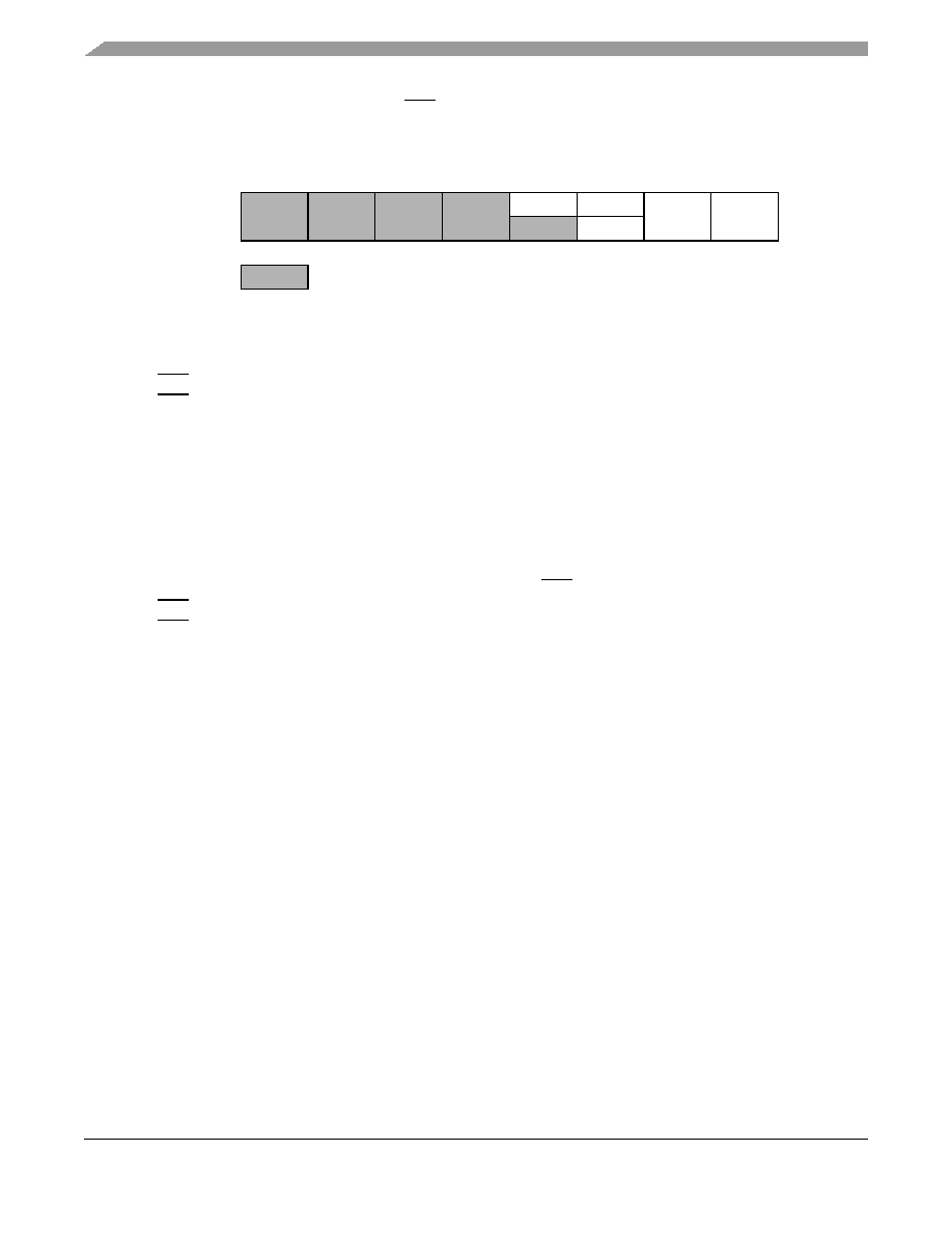
External Interrupt (IRQ)
MC68HC908LB8 Data Sheet, Rev. 0
82
Freescale Semiconductor
∑
Controls triggering sensitivity of the IRQ interrupt pin
IRQF -- IRQ Flag Bit
This read-only status bit is high when the IRQ interrupt is pending.
1 = IRQ interrupt pending
0 = IRQ interrupt not pending
ACK -- IRQ Interrupt Request Acknowledge Bit
Writing a 1 to this write-only bit clears the IRQ latch. ACK always reads as 0. Reset clears ACK.
IMASK -- IRQ Interrupt Mask Bit
Writing a 1 to this read/write bit disables IRQ interrupt requests. Reset clears IMASK.
1 = IRQ interrupt requests disabled
0 = IRQ interrupt requests enabled
MODE -- IRQ Edge/Level Select Bit
This read/write bit controls the triggering sensitivity of the IRQ pin. Reset clears MODE.
1 = IRQ interrupt requests on falling edges and low levels
0 = IRQ interrupt requests on falling edges only
Address:
$001D
Bit 7
6
5
4
3
2
1
Bit 0
Read:
IRQF
0
IMASK
MODE
Write:
ACK
Reset:
0
0
0
0
0
0
0
0
= Unimplemented
Figure 8-3. IRQ Status and Control Register (INTSCR)

MC68HC908LB8 Data Sheet, Rev. 0
Freescale Semiconductor
83
Chapter 9
Keyboard Interrupt Module (KBI)
9.1 Introduction
The keyboard interrupt module (KBI) provides seven independently maskable external interrupts which
are accessible via PTA0≠PTA6. When a port pin is enabled for keyboard interrupt function, an internal
pullup device is also enabled on the pin.
Figure 9-1. Block Diagram Highlighting KBI Block and Pins
M68HC08 CPU
CONTROL AND STATUS
USER FLASH -- 8 KBYTES
USER RAM -- 128 BYTES
MONITOR ROM -- 350 BYTES
USER FLASH VECTOR SPACE -- 34 BYTES
DDRB
PO
R
T
B
DDRC
PORT
C
INTERNAL BUS
PTA6
(1)
/AD5/TCH0/KBI6
PTA5
(1)
/RST/KBI5
PTA4
(1)
/AD4/KBI4
PTA3
(1)
/AD3/KBI3
PTA2
(1)
/AD2/KBI2
PTA1
(1)
/AD1/KBI1
PTA0
(1)
/AD0/KBI0
PTB7/V
OUT
/AD6/FAULT
(2)
PTB6/V≠
PTB5/V+
PTB4/PWM1
PTB3/PWM0
PTB2/FAULT
(2)
PTB1/BOT
PTB0/TOP
PTC1
(1)
/OSC2
PTC0
(1)
/OSC1
POWER
V
SS
V
DD
DDRA
PO
R
T
A
PTC2
(1)
/SHTDWN/IRQ
FLASH PROGRAMMING
OSCILLATOR
CPU
REGISTERS
ARITHMETIC/LOGIC
UNIT (ALU)
SYSTEM INTEGRATION
MODULE
DUAL CHANNEL PWM
MODULE
HIGH RESOLUTION PWM
MODULE
LOW-VOLTAGE INHIBIT
MODULE
COMPUTER OPERATING
PROPERLY MODULE
2-CHANNEL TIMER
MODULE
8-BIT ANALOG-TO-DIGITAL
CONVERTER MODULE
OP AMP/COMPARATOR
MODULE
KEYBOARD INTERRUPT
MODULE
MODULE
ROUTINES ROM -- 674 BYTES
REGISTERS -- 64 BYTES
1. Pin contains integrated pullup device.
2. Fault function switchable between pins PTB2 and PTB7.
Notes:

Keyboard Interrupt Module (KBI)
MC68HC908LB8 Data Sheet, Rev. 0
84
Freescale Semiconductor
9.2 Features
Features include:
∑
Seven keyboard interrupt pins with separate keyboard interrupt enable bits and one keyboard
interrupt mask
∑
Hysteresis buffers
∑
Programmable edge-only or edge- and level- interrupt sensitivity
∑
Exit from low-power modes
∑
I/O (input/output) port bit(s) software configurable with pullup device(s) if configured as input port
bit(s)
Figure 9-2. Keyboard Module Block Diagram
Addr.
Register Name
Bit 7
6
5
4
3
2
1
Bit 0
$001A
Keyboard Status and Control
Register (INTKBSCR)
See page 87.
Read:
0
0
0
0
KEYF
0
IMASKK
MODEK
Write:
ACKK
Reset:
0
0
0
0
0
0
0
0
$001B
Keyboard Interrupt Enable
Register (INTKBIER)
See page 88.
Read:
KBIE6
KBIE5
KBIE4
KBIE3
KBIE2
KBIE1
KBIE0
Write:
Reset:
0
0
0
0
0
0
0
0
= Unimplemented
Figure 9-3. I/O Register Summary
KBIE0
KBIE6
.
.
.
KEYBOARD
INTERRUPT
D
Q
CK
CLR
V
DD
MODEK
IMASKK
REQUEST
VECTOR FETCH
DECODER
ACKK
INTERNAL BUS
RESET
TO PULLUP ENABLE
KBI6
KBI0
TO PULLUP ENABLE
SYNCHRONIZER
KEYF

Functional Description
MC68HC908LB8 Data Sheet, Rev. 0
Freescale Semiconductor
85
9.3 Functional Description
Writing to the KBIE6≠KBIE0 bits in the keyboard interrupt enable register independently enables or
disables each port A pin as a keyboard interrupt pin. Enabling a keyboard interrupt pin also enables its
internal pullup device. A logic 0 applied to an enabled keyboard interrupt pin latches a keyboard interrupt
request. A keyboard interrupt is latched when one or more keyboard pins goes low after all were high.
The MODEK bit in the keyboard status and control register controls the triggering mode of the keyboard
interrupt.
∑
If the keyboard interrupt is edge-sensitive only, a falling edge on a keyboard pin does not latch an
interrupt request if another keyboard pin is already low. To prevent losing an interrupt request on
one pin because another pin is still low, software can disable the latter pin while it is low.
∑
If the keyboard interrupt is falling edge- and low-level sensitive, an interrupt request is present as
long as any keyboard interrupt pin is low and the pin is keyboard interrupt enabled.
If the MODEK bit is set, the keyboard interrupt pins are both falling edge- and low-level sensitive, and both
of the following actions must occur to clear a keyboard interrupt request:
∑
Vector fetch or software clear -- A vector fetch generates an interrupt acknowledge signal to clear
the interrupt request. Software may generate the interrupt acknowledge signal by writing a 1 to the
ACKK bit in the keyboard status and control register (INTKBSCR). The ACKK bit is useful in
applications that poll the keyboard interrupt pins and require software to clear the keyboard
interrupt request. Writing to the ACKK bit prior to leaving an interrupt service routine can also
prevent spurious interrupts due to noise. Setting ACKK does not affect subsequent transitions on
the keyboard interrupt pins. A falling edge that occurs after writing to the ACKK bit latches another
interrupt request. If the keyboard interrupt mask bit, IMASKK, is clear, the CPU loads the program
counter with the vector address at locations $FFE0 and $FFE1.
∑
Return of all enabled keyboard interrupt pins to logic 1 -- As long as any enabled keyboard
interrupt pin is at logic 0, the keyboard interrupt remains set.
The vector fetch or software clear and the return of all enabled keyboard interrupt pins to logic 1 may occur
in any order.
If the MODEK bit is clear, the keyboard interrupt pin is falling-edge-sensitive only. With MODEK clear, a
vector fetch or software clear immediately clears the keyboard interrupt request.
Reset clears the keyboard interrupt request and the MODEK bit, clearing the interrupt request even if a
keyboard interrupt pin stays at logic 0.
The keyboard flag bit (KEYF) in the keyboard status and control register can be used to see if a pending
interrupt exists. The KEYF bit is not affected by the keyboard interrupt mask bit (IMASKK) which makes
it useful in applications where polling is preferred.
To determine the logic level on a keyboard interrupt pin, use the data direction register to configure the
pin as an input and read the data register.
NOTE
Setting a keyboard interrupt enable bit (KBIEx) forces the corresponding
keyboard interrupt pin to be an input, overriding the data direction register.
However, the data direction register bit must be a 0 for software to read the
pin.

Keyboard Interrupt Module (KBI)
MC68HC908LB8 Data Sheet, Rev. 0
86
Freescale Semiconductor
9.4 Keyboard Initialization
When a keyboard interrupt pin is enabled, it takes time for the internal pullup to reach a logic 1. Therefore,
a false interrupt can occur as soon as the pin is enabled.
To prevent a false interrupt on keyboard initialization:
1.
Mask keyboard interrupts by setting the IMASKK bit in the keyboard status and control register.
2.
Enable the KBI pins by setting the appropriate KBIEx bits in the keyboard interrupt enable register.
3.
Write to the ACKK bit in the keyboard status and control register to clear any false interrupts.
4.
Clear the IMASKK bit.
An interrupt signal on an edge-triggered pin can be acknowledged immediately after enabling the pin. An
interrupt signal on an edge- and level-triggered interrupt pin must be acknowledged after a delay that
depends on the external load.
Another way to avoid a false interrupt:
1.
Configure the keyboard pins as outputs by setting the appropriate DDRA bits in data direction
register A.
2.
Write 1s to the appropriate port A data register bits.
3.
Enable the KBI pins by setting the appropriate KBIEx bits in the keyboard interrupt enable register.
9.5 Low-Power Modes
The WAIT and STOP instructions put the microcontroller unit (MCU) in low power-consumption standby
modes.
9.5.1 Wait Mode
The keyboard module remains active in wait mode. Clearing the IMASKK bit in the keyboard status and
control register enables keyboard interrupt requests to bring the MCU out of wait mode.
9.5.2 Stop Mode
The keyboard module remains active in stop mode. Clearing the IMASKK bit in the keyboard status and
control register enables keyboard interrupt requests to bring the MCU out of stop mode.
9.6 Keyboard Module During Break Interrupts
The system integration module (SIM) controls whether the keyboard interrupt latch can be cleared during
the break state. The BCFE bit in the SIM break flag control register (SBFCR) enables software to clear
status bits during the break state.
To allow software to clear the keyboard interrupt latch during a break interrupt, write a 1 to the BCFE bit.
If a latch is cleared during the break state, it remains cleared when the MCU exits the break state.
To protect the latch during the break state, write a 0 to the BCFE bit. With BCFE at 0 (its default state),
writing to the keyboard acknowledge bit (ACKK) in the keyboard status and control register during the
break state has no effect. See
9.7.1 Keyboard Status and Control Register
.

I/O Registers
MC68HC908LB8 Data Sheet, Rev. 0
Freescale Semiconductor
87
9.7 I/O Registers
These registers control and monitor operation of the keyboard module:
∑
Keyboard status and control register (INTKBSCR)
∑
Keyboard interrupt enable register (INTKBIER)
9.7.1 Keyboard Status and Control Register
The keyboard status and control register:
∑
Flags keyboard interrupt requests
∑
Acknowledges keyboard interrupt requests
∑
Masks keyboard interrupt requests
∑
Controls keyboard interrupt triggering sensitivity
Bits 7≠4 -- Not used
These read-only bits always read as 0s.
KEYF -- Keyboard Flag Bit
This read-only bit is set when a keyboard interrupt is pending. Reset clears the KEYF bit.
1 = Keyboard interrupt pending
0 = No keyboard interrupt pending
ACKK -- Keyboard Acknowledge Bit
Writing a 1 to this write-only bit clears the keyboard interrupt request. ACKK always reads as 0. Reset
clears ACKK.
IMASKK -- Keyboard Interrupt Mask Bit
Writing a 1 to this read/write bit prevents the output of the keyboard interrupt mask from generating
interrupt requests. Reset clears the IMASKK bit.
1 = Keyboard interrupt requests masked
0 = Keyboard interrupt requests not masked
MODEK -- Keyboard Triggering Sensitivity Bit
This read/write bit controls the triggering sensitivity of the keyboard interrupt pins. Reset clears
MODEK.
1 = Keyboard interrupt requests on falling edges and low levels
0 = Keyboard interrupt requests on falling edges only
9.7.2 Keyboard Interrupt Enable Register
The keyboard interrupt enable register enables or disables each port A pin to operate as a keyboard
interrupt pin.
Address: $001A
Bit 7
6
5
4
3
2
1
Bit 0
Read:
0
0
0
0
KEYF
0
IMASKK
MODEK
Write:
ACKK
Reset:
0
0
0
0
0
0
0
0
= Unimplemented
Figure 9-4. Keyboard Status and Control Register (INTKBSCR)

Keyboard Interrupt Module (KBI)
MC68HC908LB8 Data Sheet, Rev. 0
88
Freescale Semiconductor
KBIE6≠KBIE0 -- Keyboard Interrupt Enable Bits
Each of these read/write bits enables the corresponding keyboard interrupt pin to latch interrupt
requests. Reset clears the keyboard interrupt enable register.
1 = PTAx pin enabled as keyboard interrupt pin
0 = PTAx pin not enabled as keyboard interrupt pin
Address: $001B
Bit 7
6
5
4
3
2
1
Bit 0
Read:
KBIE6
KBIE5
KBIE4
KBIE3
KBIE2
KBIE1
KBIE0
Write:
Reset:
0
0
0
0
0
0
0
0
Figure 9-5. Keyboard Interrupt Enable Register (INTKBIER)

MC68HC908LB8 Data Sheet, Rev. 0
Freescale Semiconductor
89
Chapter 10
High Resolution PWM (HRP)
10.1 Introduction
The High Resolution PWM (HRP) provides two complementary outputs that can be used to control
half-bridge systems in, for example, light ballast applications. It uses a dithering control method to provide
a high step resolution (3.906 ns from an 8 MHz input clock). It also provides a shutdown input that can be
used to disable the outputs when a fault condition is detected in the application.
The pins supporting the HRP can be seen in
Figure 10-1
, and a block diagram of the HRP module is
shown in
Figure 10-3
.
10.2 Features
Features of the HRP include:
∑
One complementary output pair for driving a half bridge
∑
Dithering between two frequencies or duty cycles, for increased output resolution
∑
Automatic calculation of second frequency or duty cycle for output dithering
∑
Variable frequency mode with automatic 50% duty cycle calculation
∑
Variable duty cycle mode
∑
Programmable deadtime insertion
∑
Shutdown input for fast disabling of outputs
10.3 Pin Name Conventions
The HRP shares two output pins with two port B input/output (I/O) pins and one input pin with one port C
input pin.
Table 10-1. Pin Naming Conventions
HRP Generic Pin Name
Full HRP Pin Name
TOP
PTB0/TOP
BOT
PTB1/BOT
SHTDWN
PTC2/SHTDWN/IRQ

High Resolution PWM (HRP)
MC68HC908LB8 Data Sheet, Rev. 0
90
Freescale Semiconductor
Figure 10-1. Block Diagram Highlighting HRP Block and Pins
NOTE
Setting the HRPOE bit in the HRPCTRL register forces the corresponding
HRP output pins to be outputs, overriding the data direction register. In
order to read the states of the pins, the data direction register bit must be
a 0.
Setting the SHTEN bit in the HRPCTRL register forces the SHTDWN pin to
be an input, overriding the data direction register. In order to read the state
of the pin, the data direction register bit must be a 0.
M68HC08 CPU
CONTROL AND STATUS
USER FLASH -- 8 KBYTES
USER RAM -- 128 BYTES
MONITOR ROM -- 350 BYTES
USER FLASH VECTOR SPACE -- 34 BYTES
DDRB
PORTB
DDRC
PORTC
INTERNAL BUS
PTA6
(1)
/AD5/TCH0/KBI6
PTA5
(1)
/RST/KBI5
PTA4
(1)
/AD4/KBI4
PTA3
(1)
/AD3/KBI3
PTA2
(1)
/AD2/KBI2
PTA1
(1)
/AD1/KBI1
PTA0
(1)
/AD0/KBI0
PTB7/V
OUT
/AD6/FAULT
(2)
PTB6/V≠
PTB5/V+
PTB4/PWM1
PTB3/PWM0
PTB2/FAULT
(2)
PTB1/BOT
PTB0/TOP
PTC1
(1)
/OSC2
PTC0
(1)
/OSC1
POWER
V
SS
V
DD
DDRA
PORTA
PTC2
(1)
/SHTDWN/IRQ
FLASH PROGRAMMING
OSCILLATOR
CPU
REGISTERS
ARITHMETIC/LOGIC
UNIT (ALU)
SYSTEM INTEGRATION
MODULE
DUAL CHANNEL PWM
MODULE
HIGH RESOLUTION PWM
MODULE
LOW-VOLTAGE INHIBIT
MODULE
COMPUTER OPERATING
PROPERLY MODULE
2-CHANNEL TIMER
MODULE
8-BIT ANALOG-TO-DIGITAL
CONVERTER MODULE
OP AMP/COMPARATOR
MODULE
KEYBOARD INTERRUPT
MODULE
MODULE
ROUTINES ROM -- 674 BYTES
REGISTERS -- 64 BYTES
1. Pin contains integrated pullup device.
2. Fault function switchable between pins PTB2 and PTB7.
Notes:

Functional Description
MC68HC908LB8 Data Sheet, Rev. 0
Freescale Semiconductor
91
NOTE
When HRPMODE = 0, STEP[4:0] are mapped into the five least significant
bits of the HRPPERL register.
When HRPMODE = 1, STEP[4:0] are mapped into the five least significant
bits of the HRPDCL register.
10.4 Functional Description
Figure 10-3
provides a block diagram of the module.
Addr.
Register Name
Bit 7
6
5
4
3
2
1
Bit 0
$0051
HRP Control Register
(HRPCTRL)
See page 103.
Read:
SHTLVL
HRPOE
SHTIF
SHTIE
SHTEN
HRPMODE
HRPEN
Write:
Reset
0
0
0
0
0
0
0
$0052
HRP Duty Cycle Register
High (HRPDCH)
See page 105.
Read:
DC10
DC9
DC8
DC7
DC6
DC5
DC4
DC3
Write:
Reset
0
0
0
0
0
0
0
0
$0053
HRP Duty Cycle Register
Low (HRPDCL)
See page 105.
Read:
DC2
DC1
DC0
STEP4
STEP3
STEP3
STEP1
STEP0
Write:
Reset
0
0
0
0
0
0
0
0
$0054
HRP Period Register High
(HRPPERH)
See page 105.
Read:
P10
P9
P8
P7
P6
P5
P4
P3
Write:
Reset
0
0
0
0
0
0
0
0
$0055
HRP Period Register Low
(HRPPERL)
See page 105.
Read:
P2
P1
P0
STEP4
STEP3
STEP2
STEP1
STEP0
Write:
Reset
0
0
0
0
0
0
0
0
$0056
HRP Deadtime Register
(HRPDT)
See page 106.
Read:
DT7
DT6
DT5
DT4
DT3
DT2
DT1
DT0
Write:
Reset
0
0
0
0
1
0
0
0
$0057
HRP Timebase Register High
(HRPTBH)
See page 106.
Read:
TB15
TB14
TB13
TB12
TB11
TB10
TB9
TB8
Write:
Reset
0
0
0
0
0
0
0
0
$0058
HRP Timebase Register Low
(HRPTBL)
See page 106.
Read:
TB7
TB6
TB5
TB4
TB3
TB2
TB1
TB0
Write:
Reset
0
0
0
0
0
0
0
0
$0059
Frequency Dithering Control
Register (HRPDCR)
See page 107.
Read:
CLKSRC
SEL2
SEL1
SEL0
Write:
Reset
0
0
0
0
= Unimplemented
Figure 10-2. HRP I/O Register Summary

High Resolution PWM (HRP)
MC68HC908LB8 Data Sheet, Rev. 0
92
Freescale Semiconductor
Figure 10-3. Block Diagram of High Resolution PWM (HRP)
The HRP comprises four blocks, as follows
1.
A dual frequency generator, which generates a pair of complementary PWM output signals. It
allows dithering between two adjacent frequencies or duty cycles to increase the resolution of the
output signal. After deadtime insertion, these signals are routed to the TOP and BOT output pins
2.
A dithering controller, or timebase, which sets the dithering cycle time and the percentage of time
spent on each of the dithering frequencies or duty cycles.
3.
Two deadtime generators, for inserting deadtime into the output signals.
4.
A set of control registers
The HRP can operate in two modes.
1.
Variable Frequency Mode: for variation of the output frequency at a fixed 50% duty cycle
2.
Variable Duty Cycle Mode: for variation of the duty cycle at a fixed frequency.
10.4.1 The Principle of Frequency Dithering
Frequency dithering is an averaging technique, which can increase the resolution of an output signal by
switching between two frequencies. By varying the time spent on each frequency, the average output
frequency will be a value between the two frequencies. For example, in
Figure 10-4
a signal switches
between 10 kHz and 20 kHz over a fixed cycle time. 30% of each cycle is spent at 20 kHz, 70% at 10 kHz.
The equivalent average frequency over time is 13 kHz.
DITHERING
CONTROLLER
DUAL
FREQUENCY
GENERATOR
DEADTIME GENERATOR
DEADTIME GENERATOR
COMPLEMENTARY OUTPUTS
WITH PROGRAMMABLE DEADTIME
SHUTDOWN DETECT INPUT
FOR FAST DISABLING
OF OUTPUTS
TOP
BOT
SHTDWN
CONTROL
REGISTERS
INTERN
AL B
U
S
BUSCLK
HRPCLK

Functional Description
MC68HC908LB8 Data Sheet, Rev. 0
Freescale Semiconductor
93
Figure 10-4. Dithering Waveforms
10.4.2 Frequency Dithering on the HRP
The HRP provides frequency dithering between two signals whose periods differ by one HRPCLK cycle.
When the HRP is supplied with an 8 MHz clock, the difference between the period values is 125 ns.
The HRP provides a programmable number of dithering steps, up to a maximum of 32 steps. This results
in a maximum frequency resolution of 125/32 = 3.906 ns when using an 8 MHz clock.
Figure 10-5
shows the relationship between the two dithering frequencies and the output frequency when
32 dithering steps are chosen. In this example, the Period signal is output for 25% of the time, i.e. 8 of the
32 steps, and the Period+1 signal is output for 75% of the time, i.e. 24 of the 32 steps.
10
0
60
50
40
30
20
70
80
90
100
10 kHz
20 kHz
1 CYCLE
20 kHz
10 kHz
AVERAGE
SIGNAL
13 kHz
% CYCLE
t

High Resolution PWM (HRP)
MC68HC908LB8 Data Sheet, Rev. 0
94
Freescale Semiconductor
Figure 10-5. High Resolution PWM Dithering
10.4.3 Duty Cycle Dithering
As an alternative to frequency dithering, duty cycle dithering, where dithering occurs between two signals
having the same frequency, but with duty cycles differing by one clock period. The HRP can perform duty
cycle dithering with the same step resolution as the frequency dithering option (125/32 = 3.906 ns, with
an 8 MHz clock).
10.4.4 Frequency Generation
The dual frequency generator block contains a 16-bit up counter, which generates an output signal, based
on the values in the period register HRPPERH:HRPPERL and the duty cycle register HRPDCH:HRPDCL.
The output signal and its inverse are later fed into the deadtime generators for deadtime insertion.
Multiplexors on the inputs of the period register and the duty cycle register select between two period
(PERIOD1 and PERIOD2) and two duty cycle (DUTY1 and DUTY2) values. The values of PERIOD1,
PERIOD2, DUTY1, and DUTY2 are determined by the HRPMODE bit in the HRPCTRL register and the
contents of the HRPPERH:HRPPERL and HRPDCH:HRPDCL registers.
PERIOD1 and DUTY1 define the frequency output by the dual-frequency generator; PERIOD2 and
DUTY2 define a second output frequency, which is automatically calculated by the HRP module.
The module switches between PERIOD1/DUTY1 and PERIOD2/DUTY2.
t
PERIOD +1 = $81
PERIOD = $80
FREQUENCY = 1/ ($81 * 125 ns) = 62.015 kHz
FREQUENCY = 1/ ($80 * 125 ns) = 62.500 kHz
STEPS
0
8
16
24
PERIOD = $80
PERIOD +1 = $81
AVERAGE FREQUENCY = 62.015 + ((62.500 ≠ 62.015)/32 * 8) = 62.136 kHz
0
16
24
8
0

Functional Description
MC68HC908LB8 Data Sheet, Rev. 0
Freescale Semiconductor
95
The rate of switching is controlled by the dithering controller, and is dependent on the values of the
CLKSRC bit and the SEL[2:0] bits in the HRPDCR register, the contents of the HRPTBH:HRPTBL
registers, and, depending on the value of the HRPMODE bit, the five least significant bits in the HRPPERL
or HRPDCL registers.
For more detailed information, see
10.4.7 Dithering Controller
.
Table 10-2. HRPMODE Bit Options
HRPMODE
Mode
PERIOD1
PERIOD2
DUTY1
DUTY2
0
Variable
Frequency
P[10:0]
P[10:0] +1
PERIOD1/2
PERIOD2/2
1
Variable Duty
Cycle
P[10:0]
P[10:0]
DC[10:0]
DC[10:0] +1

Figure 10-6. Dithering Controller and Dual Frequency Generator Block
HRPTBH
HRPTBL
COMPARE
16-BIT COUNTER
DIVIDER
COMPARE
COMPARE
MODULUS
5-BIT
COUNTER
S
R
Q
F
R
E
Q
UE
NC
Y
DUTY CYCLE REGISTER
UP COUNTER
PERIOD REGISTER
DC[10:0]
P[10:0]
HRPMODE
DUAL FREQUENCY GENERATOR
DITHERING TIMEBASE
+1
/2
/2
TO DEADTIME
GENERATORS
SE
L
E
CT
1
0
0
1
1
0
0
1
1
0
RESET
HRPCLK
+1
DUTY 1
DUTY 2
PERIOD 1
PERIOD 2
STEP[4:0]
SEL[2:0]
0
1
INCREMENT
CLK
SRC
CLKSEL = 0, clock from dual frequency generator
CLKSEL = 1, clock from 16-bit timebase counter

Functional Description
MC68HC908LB8 Data Sheet, Rev. 0
Freescale Semiconductor
97
10.4.5 Variable Frequency Mode (HRPMODE = 0)
Variable frequency mode is selected when HRPMODE = 0. In this mode the period of the output signal
can be varied, while keeping the duty cycle fixed at 50%.
PERIOD1, PERIOD2, DUTY1, and DUTY2 are calculated from bits P[10:0] in registers
HRPPERH:HRPPERL to produce two frequencies having periods differing by one clock cycle but both
with 50% duty cycles.
Table 10-2
lists the period and duty cycle values based on the HRPMODE bit.
The scaled value in STEP[4:0] (the five least significant bits of HRPPERH:HRPPERL) specifies how
many of the selected number of steps are spent on the longer period (PERIOD2). For more detailed
information, see
10.4.7 Dithering Controller
.
The formula for calculating the average output period in variable frequency mode (including dithering) is:
(EQ 10-1)
where the function INT() represents the integer part of the operand, and 2
SEL[2:0]
is the STEP[4:0] scaling
factor.
In Variable Frequency Mode, the individual periods and duty cycles are given by:
(EQ 10-2)
(EQ 10-3)
(EQ 10-4)
(EQ 10-5)
10.4.6 Variable Duty Cycle Mode (HRPMODE = 1)
Variable duty cycle mode is selected when HRPMODE = 1. This mode allows dithering to be achieved by
varying the duty cycle of the output waveform while keeping the period fixed.
In this mode, the period of both PERIOD1 and PERIOD2 are identical. DUTY2 is automatically set to
DUTY1 + 1. This provides two signals with the same frequency but with duty cycles differing by one bus
clock cycle. Dithering between these two signals can increase the resolution of the output by a factor of
up to 32.
The scaled value in STEP[4:0] (the five least significant bits of HRPDCH:HRPDCL) specifies how many
of the selected number of steps are spent on the longer duty cycle, DUTY2.
For more detailed information, see
10.4.7 Dithering Controller
.
Output Period (seconds)
P 10:0
[
]
HRPCLK
------------------------
INT
STEP 4:0
[
]
2
SEL[2:0]
-----------------------------
32
2
SEL[2:0]
-------------------
HRPCLK
•
--------------------------------------------------
+
=
PERIOD1
P[10:0]
HRPCLK
------------------------
=
DUTY1
PERIOD1
2
--------------------------
50% duty cycle
=
=
59PERIOD2
P[10:0]
1
+
HRPCLK
---------------------------
=
DUTY2
PERIOD2
2
--------------------------
50% duty cycle
=
=

High Resolution PWM (HRP)
MC68HC908LB8 Data Sheet, Rev. 0
98
Freescale Semiconductor
The formula for calculating the output duty cycle in variable duty cycle mode is:
(EQ 10-6)
where 2
SEL[2:0]
is the STEP[4:0] scaling factor.
In Variable Duty Cycle Mode, the individual periods and duty cycles are given by:
(EQ 10-7)
(EQ 10-8)
(EQ 10-9)
(EQ 10-10)
10.4.7 Dithering Controller
The dithering controller consists of a 5-bit counter with programmable modulus. The counter contents are
compared with a scaled version of the STEP[4:0] bits.
The modulus value (i.e., the total number of steps) and the STEP[4:0] scaling factor are set by the SEL
bits in the HRP configuration register.
Table 10-3
lists the available options. Note that the scaling of the
STEP[4:0] bits is linked to the modulus value. For example, if a modulus of 32 is chosen, STEP[4:0] is not
scaled (32 steps of dithering are available). If a modulus of 16 is chosen, STEP[4:0] is divided by 2, so
that only 16 steps of dithering are available.
For example, if you decide to have 16 steps (SEL = 1) instead of the maximum of 32, and you set
STEP[4:0] equal to 23, then the scaled value of STEP will be 11 (i.e., the integer part of 23 divided by 2).
If you decide to have 4 steps instead of 32, the scaled value of 23 would be 2 (the integer part of 23 divided
by 8).
Table 10-3. Number of Steps and Step Scaling
SEL
Number of Steps
Divide STEP[4:0] by...
0
32
1
1
16
2
2
8
4
3
4
8
4
2
16
5
0
32
6
Reserved
Reserved
7
Reserved
Reserved
Output Duty Cycle
DC 10:0
[
]
HRPCLK
-------------------------
INT
STEP 4:0
[
]
2
SEL[2:0]
-----------------------------
32
2
SEL[2:0]
-------------------
HRPCLK
•
--------------------------------------------------
+
=
PERIOD1
P[10:0]
HRPCLK
------------------------
=
DUTY1
DC[10:0]
=
PERIOD2
PERIOD1
P[10:0]
HRPCLK
------------------------
=
=
DUTY2
DUTY1
1
+
DC[10:0]
1
+
=
=

Functional Description
MC68HC908LB8 Data Sheet, Rev. 0
Freescale Semiconductor
99
STEP[4:0] is read from register HRPPERL (if HRPMODE = 0) or from register HRPDCL (if HRPMODE =
1). See
10.4.4 Frequency Generation
for more detailed information on the HRPMODE bit. Thus, by
varying the value of STEP[4:0], the programmer can vary the output signal.
10.4.8 Dithering Controller Timebase
The 5-bit counter may be clocked from the dual frequency generator counter or from a 16-bit timebase.
The clock source is selected by the CLKSRC bit in the HRPDCR register.
Clocking from the dual frequency generator sets the timebase for each dithering step equal to the period
of the HRP output waveform.
Clocking from the 16-bit timebase allows longer or shorter timebases to be used. This allows the system
designer to set the switching frequency to a certain value, to avoid undesirable harmonics or beat
frequencies.
Table 10-4
shows the clock options and corresponding timebase values.
10.4.9 Deadtime Insertion
The deadtime generators receive the two output signals TOP and BOT from the dual frequency generator
block.
Deadtime is incorporated into these signals on each positive edge by delaying the positive edge for a
number of clock cycles. The number of clock cycles is equal to the value in the 8-bit HRP Deadtime
register HRPDT.
Figure 10-7
shows the relationship between the TOP and BOT input signals to the
deadtime generators, the HRPDT register contents, and the outputs from the deadtime generators.
Table 10-4. Dithering Timebase Options
CLKSEL
Clock Source
Timebase
0
Dual Frequency Generator
1
16 bit timebase
P(10:0)
HRPCLK
--------------------------
HRPTBH:HRPTBL
HRPCLK
--------------------------------------------------

High Resolution PWM (HRP)
MC68HC908LB8 Data Sheet, Rev. 0
100
Freescale Semiconductor
Figure 10-7. Deadtime Insertion Waveforms
NOTE
Care must be taken when setting the duty cycle and deadtime values to
ensure that a PWM signal appears on both TOP and BOT when using the
module to control a half bridge. It is possible to configure the HRP to output
a continuous logic 0 on TOP or BOT.
If the deadtime is equal to or greater than the duty cycle value, the BOT
output will will remain at logic 0, while TOP will output a PWM signal. (See
Figure 10-8
.)
Similarly, if the deadtime is equal to or smaller than the period minus the
duty cycle value, the TOP output will remain at logic 0, while BOT will output
a PWM signal. (See
Figure 10-9
.)
DT[7:0]
DT[7:0]
TOP IN
BOT IN
TOP OUT
BOT OUT
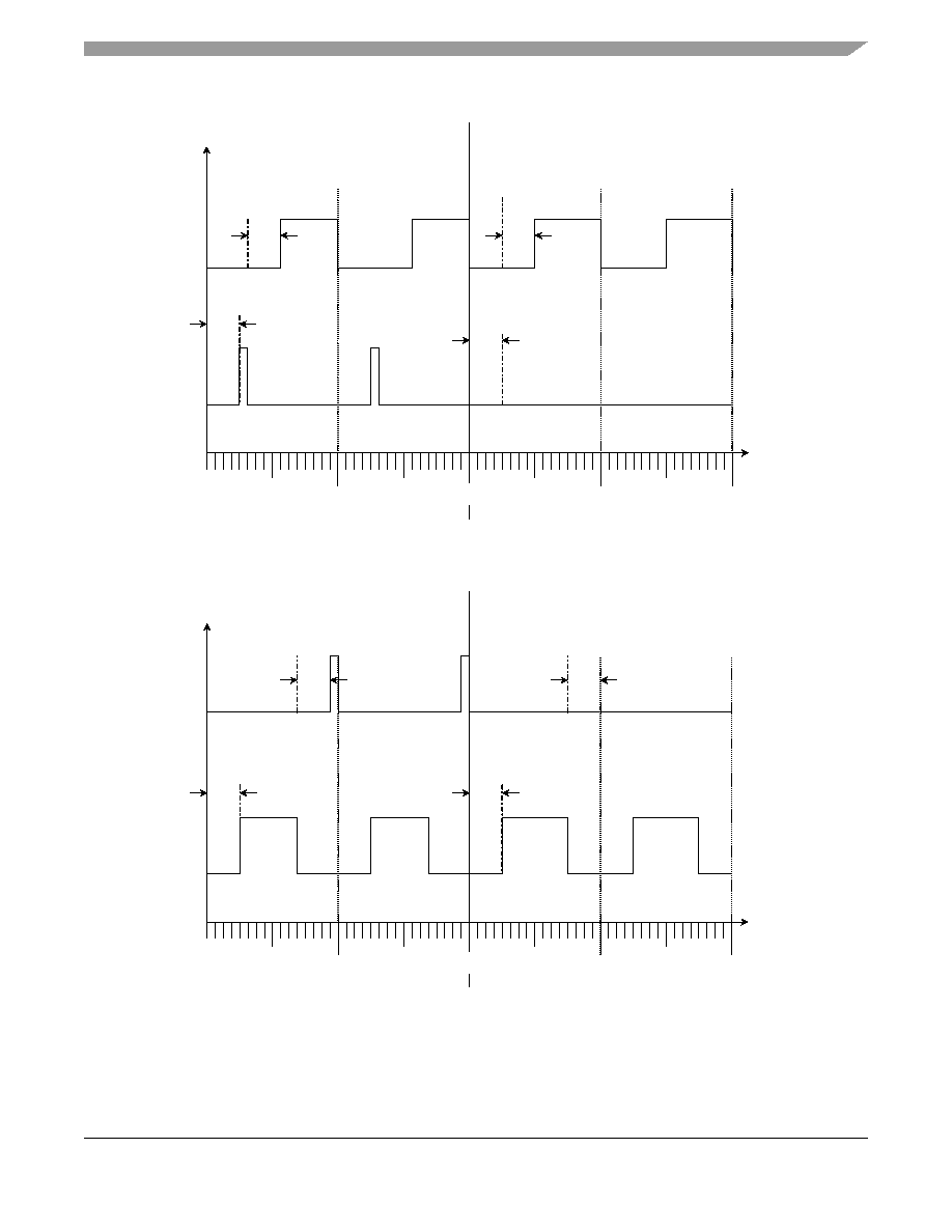
Functional Description
MC68HC908LB8 Data Sheet, Rev. 0
Freescale Semiconductor
101
Figure 10-8. Deadtime Equal to or Greater Than Duty Cycle
Figure 10-9. Deadtime Equal to or Less Than Period Minus Duty Cycle
DEADTIME
DEADTIME
16
16
0
STEP
COUNT
16
16
DEADTIME
DEADTIME
TOP
BOT
DUTY CYCLE = 5
DUTY CYCLE = 4
PERIOD = 16, DEADTIME = 4
16
DEADTIME
DEADTIME
16
0
16
16
16
STEP
COUNT
DEADTIME
DEADTIME
DUTY CYCLE = 11
DUTY CYCLE = 12
TOP
BOT
PERIOD = 16, DEADTIME = 4
16

High Resolution PWM (HRP)
MC68HC908LB8 Data Sheet, Rev. 0
102
Freescale Semiconductor
10.5 Interrupts
Setting bits SHTIE and SHTEN SHTIF in the HRP control register (HRPCTRL) configures the SHTDWN
input to generate a CPU interrupt on detection of a falling edge or a low-level on the SHTDWN pin. The
interrupt remains set until both of these events occur:
∑
The interrupt flag, SHTIF, is cleared. SHTIF is cleared by writing a logic 0 to bit SHTIF in the
HRPCTRL register.
∑
Return of the SHTDWN pin to logic 1
NOTE
While the SHTDWN pin remains low, the interrupt request remains
pending.
10.6 Low-Power Modes
10.6.1 Wait Mode
The WAIT instruction puts the MCU in low power consumption standby mode. The HRP remains active
after the execution of a WAIT instruction. In Wait mode, the HRP registers are not accessible by the CPU.
Any enabled CPU interrupt request from the HRP can bring the MCU out of Wait mode. If HRP functions
are not required during Wait mode, reduce power consumption by disabling the HRP before executing the
WAIT instruction.
10.6.2 Stop Mode
The HRP is inactive after the execution of a STOP instruction. The TOP and BOT outputs are both set to
logic 0 after execution of the STOP instruction. Entering Stop mode causes the HRPEN bit in the
HRPCTRL register to be set to 0. When the MCU exits Stop mode after an external interrupt, the HRP
resumes operation.
NOTE
The HRP shutdown pin remains active during Stop mode.
10.7 HRP During Break Interrupts
The system integration module (SIM) controls whether status bits in other modules can be cleared during
the break state. The BCFE bit in the break flag control register (BFCR) enables software to clear status
bits during the break state. See
19.2.2.5 Break Flag Control Register.
To allow software to clear status bits during a break interrupt, write a 1 to the BCFE bit. If a status bit is
cleared during the break state, it remains cleared when the MCU exits the break state. To protect status
bits during the break state, write a 0 to the BCFE bit. With BCFE at 0 (its default state), software can read
and write I/O registers during the break state without affecting status bits. Some status bits have a
two-step read/write clearing procedure. If software does the first step on such a bit before the break, the
bit cannot change during the break state as long as BCFE is at 0. After the break, doing the second step
clears the status bit.
10.7.1 Input/Output Signals
Port B shares two of its pins with the HRP. The two output pins are PTB0/TOP and PTB1/BOT. Port C
shares one of its pins (PTC2/SHTDWN/IRQ) with the HRP.
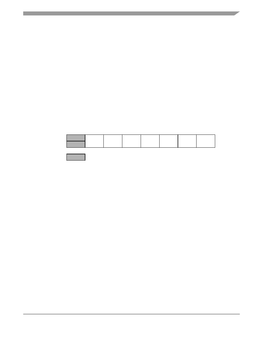
HRP Registers
MC68HC908LB8 Data Sheet, Rev. 0
Freescale Semiconductor
103
10.8 HRP Registers
The following registers control and monitor operation of the HRP:
∑
HRP control register (HRPCTRL)
∑
HRP duty cycle registers (HRPDCH: HRPDCL)
∑
HRP period registers (HRPPERH:HRPPERL)
∑
HRP deadtime register (HRPDT)
∑
HRP timebase registers (HRPTBH:HRPTBL)
10.8.1 HRP Control Register
The HRPCTRL register does the following:
∑
Enables the HRP
∑
Controls the operating mode of the HRP
∑
Enables the SHTDWN, TOP, and BOT pins
∑
Enables interrupt functionality for the SHTDWN pin
SHTLVL -- SHTDWN Pin Level
This read-only bit contains the current logic level of the SHTDWN pin. Reset clears the SHTLVL bit.
HRPOE -- HRP Output Enable
This read/write bit enables/disables the TOP and BOT output pins.
1 = Pins PTB0/TOP and PTB1/BOT function as TOP and BOT outputs from the HRP module. The
contents of the port B data and data direction registers do not affect these pins.
0 = Pins PTB0/TOP and PTB1/BOT function as PTB0 and PTB1 general-purpose I/O pins. The
state of these pins is controlled by the port B data and data direction registers.
SHTIF -- SHTDWN Interrupt Flag
This read/write bit is set when a falling edge or a low level is detected on the SHTDWN pin. Reset
clears the SHTIF bit. Writing 0 to SHTIF clears the bit.
1 = SHTDWN pin interrupt pending
0 = No SHTDWN pin interrupt pending
SHTIE -- SHTDWN Interrupt Enable
This read/write bit enables HRP CPU interrupt service requests for the SHTDWN pin. Reset clears the
SHTIE bit.
1 = SHTDWN CPU interrupt requests enabled
0 = SHTDWN CPU interrupt requests disabled
SHTEN -- Shutdown Pin Enable
Address: $0051
Bit 7
6
5
4
3
2
1
Bit 0
Read:
SHTLVL
HRPOE
SHTIF
SHTIE
SHTEN
HRP-
MODE
HRPEN
Write:
Reset:
0
0
0
0
0
0
0
= Unimplemented
Figure 10-10. HRP Control Register (HRPCTRL)

High Resolution PWM (HRP)
MC68HC908LB8 Data Sheet, Rev. 0
104
Freescale Semiconductor
This read/write bit enables the SHTDWN functionality on pin PTC2/SHTDWN/IRQ. When SHTDWN
functionality is enabled, a falling edge or a low level on the SHTDWN pin causes the TOP and BOT
outputs to be switched to logic 0 and the HRPEN bit is set to logic 0, disabling the HRP.
1 = Pin PTC2/SHTDWN/IRQ functions as SHTDWN input.
0 = Pin PTC2/SHTDWN/IRQ functions controlled by port C register
NOTE
The TOP and BOT pins must be enabled using the HRPOE bit for the
HRPEN bit to have any effect on the PTB0/TOP and PTB1/BOT I/O pins.
HRPMODE -- Mode Select
This read/write bit selects between variable frequency and variable duty cycle modes of operation.
1 = Variable duty cycle mode
0 = Variable frequency mode
HRPEN -- Enable
This read/write bit enables/disables the HRP.
1 = HRP enabled
0 = HRP disabled
When the HRP is disabled the TOP and BOT outputs both switch to logic 0. If a logic 0 is detected on the
SHTDWN input pin, the module outputs both switch to logic 0 and the HRPEN bit is automatically set to 0
to disable the module.
NOTE
The TOP and BOT pins must be enabled using the HRPOE bit for the
HRPEN bit to have any effect on the PTB0/TOP and PTB1/BOT I/O pins.
10.8.2 HRP Duty Cycle Registers
The two read/write duty cycle registers contain the 16-bit duty cycle of the output after dithering. It is split
into two parts:
1.
11-bit duty cycle value (DC[10:0]) used to generate the HRP output waveforms.
2.
5-bit step value (STEP[4:0]) that defines the percentage of time spent on the larger of two duty
cycle values in variable duty cycle mode.
The duty cycle including dithering in variable duty cycle mode is:
(EQ 10-11)
where 2
SEL[2:0]
is the STEP[4:0] scaling factor.
HRPDCH:HRPDCL are not used in variable frequency mode. The contents of the registers have no effect
in this mode
Writes to the high byte (HRPDCH) are stored in a latch until the low byte (HRPDCL) is written. Both
registers are then updated simultaneously. This prevents glitches in the output duty cycle.
Output Duty Cycle
DC 10:0
[
]
HRPCLK
-------------------------
INT
STEP 4:0
[
]
2
SEL[2:0]
-----------------------------
32
2
SEL[2:0]
-------------------
HRPCLK
•
--------------------------------------------------
+
=

HRP Registers
MC68HC908LB8 Data Sheet, Rev. 0
Freescale Semiconductor
105
DC[10:0] -- 11-Bit Duty Cycle Value
STEP[4:0] -- 5-Bit Dithering Step Value
10.8.3 HRP Period Registers
The two read/write period registers contain the 16-bit period of the PWM output after dithering. It is split
into two parts:
1.
11-bit period value (P[10:0]) used to generate the HRP's output waveforms.
2.
5-bit step value (STEP[4:0]) the lower five bits of HRPPERH:HRPPERL, specifies how much time
is spent on the longer period (PERIOD2).
The output period including dithering in variable frequency mode is:
(EQ 10-12)
where 2
SEL[2:0]
is the STEP[4:0] scaling factor.
The output period in variable duty cycle mode does not include dithering. The period value is:
(EQ 10-13)
Writes to the high byte (HRPPERH) are stored in a latch until the low byte (HRPPERL) is written. Both
registers are then updated simultaneously. This prevents glitches in the output period.
Address: HRPDCH -- $0052
HRPDCL -- $0053
Bit 15
14
13
12
11
10
9
Bit 8
Read:
DC10
DC9
DC8
DC7
DC6
DC5
DC4
DC3
Write:
Reset:
0
0
0
0
0
0
0
0
Bit 7
6
5
4
3
2
1
Bit 0
Read:
DC2
DC1
DC0
STEP4
STEP3
STEP2
STEP1
STEP0
Write:
Reset:
0
0
0
0
0
0
0
0
Figure 10-11. HRP Duty Cycle Registers (HRPDCH:HRPDCL)
Address: HRPPERH -- $0054
HRPPERL -- $0055
Bit 15
14
13
12
11
10
9
Bit 8
Read:
P10
P9
P8
P7
P6
P5
P4
P3
Write:
Reset:
0
0
0
0
0
0
0
0
Bit 7
6
5
4
3
2
1
Bit 0
Figure 10-12. HRP Period Registers (HRPPERH:HRPPERL)
Output Period (seconds)
P 10:0
[
]
HRPCLK
------------------------
INT
STEP 4:0
[
]
2
SEL[2:0]
-----------------------------
32
2
SEL[2:0]
-------------------
HRPCLK
•
--------------------------------------------------
+
=
Period
P[10:0]
HRPCLK
--------------------------
=

High Resolution PWM (HRP)
MC68HC908LB8 Data Sheet, Rev. 0
106
Freescale Semiconductor
P[10:0] -- 11-Bit Period Value
STEP[4:0] -- 5-Bit Dithering Step Value
10.8.4 HRP Deadtime Register
This read/write register contains an 8-bit value corresponding to the number of HRPCLK cycles that will
be subtracted from the logic 1 level of the TOP and BOT output signals to provide deadtime between the
two signals.
(EQ 10-14)
10.8.5 Frequency Dithering HRP Timebase Registers
The two read/write frequency dithering timebase registers HRPTBH:HRPTBL contain a 16-bit value used
to determine the time base for switching between the two dithering frequencies. The timebase is
calculated from the following formula:
(EQ 10-15)
Writes to the high byte (HRPTBH) are stored in a latch until the low byte (HRPTBL) is written. Both
registers are then updated simultaneously. This prevents glitches occurring on the output signal.
Read:
P2
P1
P0
STEP4
STEP3
STEP2
STEP1
STEP0
Write:
Reset:
0
0
0
0
0
0
0
0
Address: $0056
Bit 7
6
5
4
3
2
1
Bit 0
Read:
DT7
DT6
DT5
DT4
DT3
DT2
DT1
DT0
Write:
Reset:
0
0
0
0
1
0
0
0
Figure 10-13. HRP Deadtime Register (HRPDT)
Address: HRPTBH -- $0057
HRPTBL -- $0058
Bit 15
14
13
12
11
10
9
Bit 8
Read:
TB15
TB14
TB13
TB12
TB11
TB10
TB9
TB8
Write:
Reset:
0
0
0
0
0
0
0
0
Bit 7
6
5
4
3
2
1
Bit 0
Read:
TB7
TB6
TB5
TB4
TB3
TB2
TB1
TB0
Write:
Reset:
0
0
0
0
0
0
0
0
Figure 10-14. HRP Timebase Registers (HRPTBH:HRPTBL)
Figure 10-12. HRP Period Registers (HRPPERH:HRPPERL)
Dead Time
HRPDT
HRPCLK
--------------------------
=
Frequency Dithering Timebase (seconds)
HRPTBH:HRPTBL
HRPCLK
--------------------------------------------------
=

HRP Registers
MC68HC908LB8 Data Sheet, Rev. 0
Freescale Semiconductor
107
10.8.6 Frequency Dithering Control Register
This read/write register selects the clock source for the dithering controller, and selects the number of
dithering steps and modulus value of the dithering counter.
CLKSRC -- Dithering Clock Source
This read/write bit selects the clock source for the 5-bit dithering counter.
1 = The dithering counter is clocked from the 16-bit timebase
0 = The dithering counter is clocked from the output of the dual frequency generator counter
SEL[2:0] -- Dithering Step/Modulus Select
These read/write bits select the number of steps used by the dithering counter and set the scaling
factor for the STEP[4:0] bits.
Address: $0059
Bit 15
14
13
12
11
10
9
Bit 8
Read:
CLKSRC
SEL2
SEL1
SEL0
Write:
Reset:
0
0
0
0
= Unimplemented
Figure 10-15. Frequency Dithering Control Register (HRPDCR)
Table 10-5
CLKSEL
Clock Source
Timebase
0
Dual Frequency Generator
1
16 bit timebase
Table 10-6
SEL[2:0]
Number of Steps
Divide STEP[4:0] by...
0
32
1
1
16
2
2
8
4
3
4
8
4
2
16
5
(1)
NOTES:
1. No dithering occurs for this setting.
0
32
6
Reserved
Reserved
7
Reserved
Reserved
P(10:0)
HRPCLK
--------------------------
HRPTBH:HRPTBL
HRPCLK
--------------------------------------------------

High Resolution PWM (HRP)
MC68HC908LB8 Data Sheet, Rev. 0
108
Freescale Semiconductor
10.9 HRP Programming Examples
The HRP has been designed to simplify the software required to generate typical control waveforms and
reduce the CPU load.
The following examples show how to calculate the register values needed to generate the desired output
frequencies, resolutions, deadtime, etc. The examples consider only the case of variable frequency
mode, but the calculations for variable duty cycle mode are very similar.
Example 1
This example shows how to configure the module to output a frequency of 132.073 kHz, with an HRPCLK
of 8 MHz.
(EQ 10-16)
(EQ 10-17)
and
(EQ 10-18)
If we use 32 steps, simplifying the last equation gives
(EQ 10-19)
Therefore,
(EQ 10-20)
If we choose STEP[4:0] = 19, the output frequency = 132.026 kHz.
If we choose STEP[4:0] = 18, the output frequency = 132.094 kHz.
So STEP[4:0] = 19 gets us closer to our desired frequency of 132.073 kHz
In this case, the switching frequency is 132.094 kHz/32 = 4.1279 kHz.
Period (seconds)
10
3
≠
132.073
---------------------
7.57157
10
6
≠
•
P 10:0
[
]
8
10
6
•
--------------------
INT
STEP 4:0
[
]
2
SEL[2:0]
-----------------------------
32
2
SEL[2:0]
-------------------
8
10
6
•
•
---------------------------------------------
+
=
=
=
P 10:0
[
]
INT
STEP 4:0
[
]
2
SEL[2:0]
-----------------------------
32
2
SEL[2:0]
-------------------
---------------------------------------------
+
7.57157
8
•
60.5725
60
0.5725
+
=
=
=
P 10:0
[
]
60
$3C
=
=
INT
STEP 4:0
[
]
2
SEL[2:0]
-----------------------------
32
2
SEL[2:0]
-------------------
---------------------------------------------
0.5725
=
STEP 4:0
[
]
32
-----------------------------
0.5725
=
STEP 4:0
[
]
0.5725
32
•
18.32
18 or 19
=
=
=

HRP Programming Examples
MC68HC908LB8 Data Sheet, Rev. 0
Freescale Semiconductor
109
Example 2
This example shows how to configure the module to output a frequency of 81.5 kHz, with a deadtime of
10 µs. The system has an HRPCLK of 8 MHz, and the switching frequency must be less than 100 Hz.
(EQ 10-21)
(EQ 10-22)
and
(EQ 10-23)
If we use 32 steps, simplifying the last equation gives
(EQ 10-24)
(EQ 10-25)
If we choose STEP[4:0] = 5, the output frequency = 81.5027 kHz.
In this case (using the output of the dual frequency generator as source for the dithering timebase),
(EQ 10-26)
To achieve a switching frequency of less than 100 Hz, we must use the 16-bit timebase counter as the
source for the dithering timebase.
(EQ 10-27)
(EQ 10-28)
To insert a 10 µs deadtime in the output signals, we must calculate the value to store in the HRPDT
register from the following equation.
(EQ 10-29)
(EQ 10-30)
i.e.
(EQ 10-31)
Period (seconds)
10
3
≠
81.5
-----------
12.2699
10
6
≠
•
P 10:0
[
]
8
10
6
•
--------------------
INT
STEP 4:0
[
]
2
SEL[2:0]
-----------------------------
32
2
SEL[2:0]
-------------------
8
10
6
•
•
---------------------------------------------
+
=
=
=
P 10:0
[
]
INT
STEP 4:0
[
]
2
SEL[2:0]
-----------------------------
32
2
SEL[2:0]
-------------------
---------------------------------------------
+
12.2699
8
•
98.1592
98
0.1592
+
=
=
=
P 10:0
[
]
98
$62
=
=
INT
STEP 4:0
[
]
2
SEL[2:0]
-----------------------------
32
2
SEL[2:0]
-------------------
---------------------------------------------
0.1592
=
STEP 4:0
[
]
32
-----------------------------
0.1592
=
STEP 4:0
[
]
0.1592
32
•
5.094
5 or 6
=
=
=
Switching Frequency
Output Frequency
2
SEL
------------------------------------------------
81.5027
32
---------------------
2.5469 kHz
=
=
=
Switching Frequency
HRPCLK
HRPTB
2
•
SEL
----------------------------------------
=
HRPTB
HRPCLK
100
2
•
SEL
----------------------------
8
10
6
•
100
32
•
-----------------------
2500
$9C4
=
=
=
=
Dead Time
HRPDT
HRPCLK
--------------------------
=
10
10
6
≠
•
HRPDT
8
10
6
•
--------------------
=
HRPDT
10
8
•
80
$50
=
=
=

High Resolution PWM (HRP)
MC68HC908LB8 Data Sheet, Rev. 0
110
Freescale Semiconductor

MC68HC908LB8 Data Sheet, Rev. 0
Freescale Semiconductor
111
Chapter 11
Low-Power Modes
11.1 Introduction
The microcontroller (MCU) may enter two low-power modes: wait mode and stop mode. They are
common to all HC08 MCUs and are entered through instruction execution. This section describes how
each module acts in the low-power modes.
11.1.1 Wait Mode
The WAIT instruction puts the MCU in a low-power standby mode in which the central processor unit
(CPU) clock is disabled but the bus clock continues to run. Power consumption can be further reduced by
disabling the low-voltage inhibit (LVI) module through bits in the CONFIG1 register. See
Chapter 5
Configuration Register (CONFIG)
.
11.1.2 Stop Mode
Stop mode is entered when a STOP instruction is executed. The CPU clock is disabled and the bus clock
is disabled.
11.2 Analog-to-Digital Converter (ADC)
11.2.1 Wait Mode
The analog-to-digital converter (ADC) continues normal operation during wait mode. Any enabled CPU
interrupt request from the ADC can bring the MCU out of wait mode. If the ADC is not required to bring
the MCU out of wait mode, power down the ADC by setting ADCH4≠ADCH0 bits in the ADC status and
control register before executing the WAIT instruction.
11.2.2 Stop Mode
The ADC module is inactive after the execution of a STOP instruction. Any pending conversion is aborted.
ADC conversions resume when the MCU exits stop mode after an external interrupt. Allow one
conversion cycle to stabilize the analog circuitry.
11.3 Break Module (BRK)
11.3.1 Wait Mode
If enabled, the break (BRK) module is active in wait mode. In the break routine, the user can subtract one
from the return address on the stack if the SBSW bit in the break status register is set.

Low-Power Modes
MC68HC908LB8 Data Sheet, Rev. 0
112
Freescale Semiconductor
11.3.2 Stop Mode
The break module is inactive in stop mode. The STOP instruction does not affect break module register
states.
11.4 Central Processor Unit (CPU)
11.4.1 Wait Mode
The WAIT instruction:
∑
Clears the interrupt mask (I bit) in the condition code register, enabling interrupts. After exit from
wait mode by interrupt, the I bit remains clear. After exit by reset, the I bit is set.
∑
Disables the CPU clock
11.4.2 Stop Mode
The STOP instruction:
∑
Clears the interrupt mask (I bit) in the condition code register, enabling external interrupts. After
exit from stop mode by external interrupt, the I bit remains clear. After exit by reset, the I bit is set.
∑
Disables the CPU clock
After exiting stop mode, the CPU clock begins running after the oscillator stabilization delay.
11.5 Computer Operating Properly Module (COP)
11.5.1 Wait Mode
The COP remains active during wait mode. If COP is enabled, a reset will occur at COP timeout.
11.5.2 Stop Mode
Stop mode turns off the COPCLK input to the COP and clears the COP prescaler. Service the COP
immediately before entering or after exiting stop mode to ensure a full COP timeout period after entering
or exiting stop mode.
The STOP bit in the CONFIG1 register enables the STOP instruction. To prevent inadvertently turning off
the COP with a STOP instruction, disable the STOP instruction by clearing the STOP bit.
11.6 External Interrupt Module (IRQ)
11.6.1 Wait Mode
The external interrupt (IRQ) module remains active in wait mode. Clearing the IMASK bit in the IRQ status
and control register enables IRQ CPU interrupt requests to bring the MCU out of wait mode if IRQ function
is enabled.
11.6.2 Stop Mode
The IRQ module remains active in stop mode. Clearing the IMASK bit in the IRQ status and control
register enables IRQ CPU interrupt requests to bring the MCU out of stop mode.

Keyboard Interrupt Module (KBI)
MC68HC908LB8 Data Sheet, Rev. 0
Freescale Semiconductor
113
11.7 Keyboard Interrupt Module (KBI)
11.7.1 Wait Mode
The keyboard interrupt (KBI) module remains active in wait mode. Clearing the IMASKK bit in the
keyboard status and control register enables keyboard interrupt requests to bring the MCU out of wait
mode.
11.7.2 Stop Mode
The keyboard module remains active in stop mode. Clearing the IMASKK bit in the keyboard status and
control register enables keyboard interrupt requests to bring the MCU out of stop mode.
11.8 High Resolution PWM (HRP)
11.8.1 Wait Mode
The HRP remains active after the execution of a WAIT instruction. In wait mode the HRP registers are not
accessible by the CPU. Any enabled CPU interrupt request from the HRP can bring the MCU out of wait
mode. If HRP functions are not required during wait mode, reduce power consumption by stopping the
HRP before executing the WAIT instruction.
11.8.2 Stop Mode
The HRP is inactive after the execution of a STOP instruction. The TOP and BOT outputs are both set to
logic 0 and the HRPEN bit in the HRPCTRL register is set to 0 after execution of the STOP instruction.
The STOP instruction does not affect other register conditions or the state of the HRP counters. When
the MCU exits stop mode after an external interrupt, the HRP is inactive because the HRPEN bit is set to
0.
NOTE
The HRP shutdown pin remains active during Stop mode.
11.9 Low-Voltage Inhibit Module (LVI)
11.9.1 Wait Mode
If enabled, the low-voltage inhibit (LVI) module remains active in wait mode. If enabled to generate resets,
the LVI module can generate a reset and bring the MCU out of wait mode.
11.9.2 Stop Mode
If enabled, the LVI module remains active in stop mode. If enabled to generate resets, the LVI module
can generate a reset and bring the MCU out of stop mode.

Low-Power Modes
MC68HC908LB8 Data Sheet, Rev. 0
114
Freescale Semiconductor
11.10 Op Amp/Comparator
11.10.1 Wait Mode
While in WAIT the state of the op amp/comparator cannot be changed. If the op amp/comparator module
is not needed during wait mode, reduce power consumption by disabling the op amp/comparator before
executing the WAIT command.
11.10.2 Stop Mode
The op amp/comparator is inactive after execution of the STOP command. The op amp/comparator will
be in a low-power state and will not drive its output pin. When the MCU exits stop mode after and external
interrupt, the op amp/comparator continues operation.
11.11 Oscillator Module (OSC)
11.11.1 Wait Mode
The WAIT instruction has no effect on the oscillator logic. BUSCLKX2 and BUSCLKX4 continue to drive
to the SIM module.
11.11.2 Stop Mode
The STOP instruction disables either the XTALCLK, the RCCLK, or INTCLK output, hence BUSCLKX2
and BUSCLKX4.
11.12 Pulse-Width Modulator Module (PWM)
11.12.1 Wait Mode
When the microcontroller is put in low-power wait mode via the WAIT instruction, all clocks to the PWM
module will continue to run. If an interrupt is issued from the PWM module (via a reload or a fault), the
microcontroller will exit wait mode.
Clearing the PWMEN bit before entering wait mode will reduce power consumption in wait mode because
the counter, prescaler divider, and LDFQ divider will no longer be clocked. In addition, power will be
reduced because the PWMs will no longer toggle.
11.12.2 Stop Mode
When the microcontroller is put into stop mode via the STOP instruction, the PWM will stop functioning.
The PWM0 and PWM1 outputs are set to logic 0. The STOP instruction does not affect the register
conditions or the state of the PWM counters. When the MCU exits stop mode after an external interrupt
the PWM resumes operation.

Timer Interface Module (TIM)
MC68HC908LB8 Data Sheet, Rev. 0
Freescale Semiconductor
115
11.13 Timer Interface Module (TIM)
11.13.1 Wait Mode
The timer interface module (TIM) remains active in wait mode. Any enabled CPU interrupt request from
the TIM can bring the MCU out of wait mode.
If TIM functions are not required during wait mode, reduce power consumption by stopping the TIM before
executing the WAIT instruction.
11.13.2 Stop Mode
The TIM is inactive in stop mode. The STOP instruction does not affect register states or the state of the
TIM counter. TIM operation resumes when the MCU exits stop mode after an external interrupt.
11.14 Exiting Wait Mode
These events restart the CPU clock and load the program counter with the reset vector or with an interrupt
vector:
∑
External reset -- A logic 0 on the RST pin resets the MCU and loads the program counter with the
contents of locations: $FFFF and $FFFE.
∑
External interrupt -- A high-to-low transition on an external interrupt pin (IRQ pin) loads the
program counter with the contents of locations: $FFFB and $FFFA.
∑
Break (BRK) interrupt -- A break interrupt loads the program counter with the contents of: $FFFD
and $FFFC.
∑
Computer operating properly (COP) module reset -- A timeout of the COP counter resets the MCU
and loads the program counter with the contents of: $FFFF and $FFFE.
∑
Low-voltage inhibit (LVI) module reset -- A power supply voltage below the V
TRIPF
voltage resets
the MCU and loads the program counter with the contents of locations: $FFFF and $FFFE.
∑
Keyboard interrupt (KBI) module -- A CPU interrupt request from the KBI module loads the
program counter with the contents of: $FFE1 and $FFE0.
∑
Timer interface (TIM) module interrupt -- A CPU interrupt request from the TIM loads the program
counter with the contents of:
≠
$FFF3 and $FFF2; TIM overflow
≠
$FFF5 and $FFF4; TIM channel 1
≠
$FFF7 and $FFF6; TIM channel 0
∑
Analog-to-digital converter (ADC) module interrupt -- A CPU interrupt request from the ADC loads
the program counter with the contents of: $FFDF and $FFDE.
∑
Pulse-Width Modulator with Fault Input (PWM) -- A CPU interrupt request from the PWM load the
program counter with the contents of:
≠
$FFF1 and $FFF0; FAULT
≠
$FFEF and $FFEE; PWMINT
∑
High Resolution PWM (HRP) -- A CPU interrupt request from the HRP loads the program counter
with the contents of: $FFED and $FFEC

Low-Power Modes
MC68HC908LB8 Data Sheet, Rev. 0
116
Freescale Semiconductor
11.15 Exiting Stop Mode
These events restart the system clocks and load the program counter with the reset vector or with an
interrupt vector:
∑
External reset -- A logic 0 on the RST pin resets the MCU and loads the program counter with the
contents of locations $FFFF and $FFFE.
∑
External interrupt -- A high-to-low transition on an external interrupt pin loads the program counter
with the contents of locations:
≠
$FFFB and $FFFA; IRQ pin
≠
$FFE1 and $FFE0; keyboard interrupt pins
∑
Low-voltage inhibit (LVI) reset -- A power supply voltage below the LVI
TRIPF
voltage resets the
MCU and loads the program counter with the contents of locations $FFFF and $FFFE.
∑
Break (BRK) interrupt -- A break interrupt loads the program counter with the contents of locations
$FFFD and $FFFC.
∑
Keyboard (KBI) interrupt -- A keyboard interrupt loads the program counter with contents of
location $FFE1
and
$FFE0
.
Upon exit from stop mode, the system clocks begin running after an oscillator stabilization delay. A 12-bit
stop recovery counter inhibits the system clocks for 4096 BUSCLKX4 cycles after the reset or external
interrupt.
The short stop recovery bit, SSREC, in the CONFIG1 register controls the oscillator stabilization delay
during stop recovery. Setting SSREC reduces stop recovery time from 4096 BUSCLKX4 cycles to 32
BUSCLKX4 cycles.
NOTE
Use the full stop recovery time (SSREC = 0) in applications that use an
external crystal.

MC68HC908LB8 Data Sheet, Rev. 0
Freescale Semiconductor
117
Chapter 12
Low-Voltage Inhibit (LVI)
12.1 Introduction
This section describes the low-voltage inhibit (LVI) module, which monitors the voltage on the V
DD
pin
and can force a reset when the V
DD
voltage falls below the LVI trip falling voltage, V
TRIPF
.
12.2 Features
Features of the LVI module include:
∑
Programmable LVI reset
∑
Programmable power consumption
∑
Selectable LVI trip voltage
∑
Programmable stop mode operation
12.3 Functional Description
Figure 12-1
shows the structure of the LVI module. LVISTOP, LVIPWRD, and LVIRSTD are user
selectable options found in the configuration register (CONFIG1). See
Chapter 5 Configuration Register
(CONFIG)
.
Figure 12-1. LVI Module Block Diagram
LOW V
DD
DETECTOR
LVIPWRD
STOP INSTRUCTION
LVISTOP
LVI RESET
LVIOUT
V
DD
> LVITRIP = 0
V
DD
LVITRIP = 1
FROM CONFIG
FROM CONFIG
V
DD
FROM CONFIG
LVIRSTD

Low-Voltage Inhibit (LVI)
MC68HC908LB8 Data Sheet, Rev. 0
118
Freescale Semiconductor
The LVI is enabled out of reset. The LVI module contains a bandgap reference circuit and comparator.
Clearing the LVI power disable bit, LVIPWRD, enables the LVI to monitor V
DD
voltage. Clearing the LVI
reset disable bit, LVIRSTD, enables the LVI module to generate a reset when V
DD
falls below a voltage,
V
TRIPF
. Setting the LVI enable in stop mode bit, LVISTOP, enables the LVI to operate in stop mode.
Once an LVI reset occurs, the MCU remains in reset until V
DD
rises above a voltage, V
TRIPR
, which
causes the MCU to exit reset. See
Chapter 17 System Integration Module (SIM)
for the reset recovery
sequence.
The output of the comparator controls the state of the LVIOUT flag in the LVI status register (LVISR) and
can be used for polling LVI operation when the LVI reset is disabled.
12.3.1 Polled LVI Operation
In applications that can operate at V
DD
levels below the V
TRIPF
level, software can monitor V
DD
by polling
the LVIOUT bit. In the configuration register, the LVIPWRD bit must be at 0 to enable the LVI module, and
the LVIRSTD bit must be at 1 to disable LVI resets.
12.3.2 Forced Reset Operation
In applications that require V
DD
to remain above the V
TRIPF
level, enabling LVI resets allows the LVI
module to reset the MCU when V
DD
falls below the V
TRIPF
level. In the configuration register, the
LVIPWRD and LVIRSTD bits must be at 0 to enable the LVI module and to enable LVI resets.
12.3.3 Voltage Hysteresis Protection
Once the LVI has triggered (by having V
DD
fall below V
TRIPF
), the LVI will maintain a reset condition until
V
DD
rises above the rising trip point voltage, V
TRIPR
. This prevents a condition in which the MCU is
continually entering and exiting reset if V
DD
is approximately equal to V
TRIPF
. V
TRIPR
is greater than
V
TRIPF
by the hysteresis voltage, V
HYS
.

LVI Status Register
MC68HC908LB8 Data Sheet, Rev. 0
Freescale Semiconductor
119
12.4 LVI Status Register
The LVI status register (LVISR) indicates if the V
DD
voltage was detected below the V
TRIPF
level while
LVI resets have been disabled.
LVIOUT -- LVI Output Bit
This read-only flag becomes set when the V
DD
voltage falls below the V
TRIPF
trip voltage and is cleared
when V
DD
voltage rises above V
TRIPR
. The difference in these threshold levels results in a hysteresis
that prevents oscillation into and out of reset (see
Table 12-1
). Reset clears the LVIOUT bit.
12.5 LVI Interrupts
The LVI module does not generate interrupt requests.
12.6 Low-Power Modes
The STOP and WAIT instructions put the MCU in low power- consumption standby modes.
12.6.1 Wait Mode
If enabled, the LVI module remains active in wait mode. If enabled to generate resets, the LVI module can
generate a reset and bring the MCU out of wait mode.
12.6.2 Stop Mode
When the LVIPWRD bit in the configuration register is cleared and the LVISTOP bit in the configuration
register is set, the LVI module remains active in stop mode. If enabled to generate resets, the LVI module
can generate a reset and bring the MCU out of stop mode.
Address: $FE0C
Bit 7
6
5
4
3
2
1
Bit 0
Read:
LVIOUT
0
0
0
0
0
0
R
Write:
Reset:
0
0
0
0
0
0
0
0
= Unimplemented
R
= Reserved
Figure 12-2. LVI Status Register (LVISR)
Table 12-1. LVIOUT Bit Indication
V
DD
LVIOUT
V
DD
> V
TRIPR
0
V
DD
< V
TRIPF
1
V
TRIPF
< V
DD
< V
TRIPR
Previous value

Low-Voltage Inhibit (LVI)
MC68HC908LB8 Data Sheet, Rev. 0
120
Freescale Semiconductor

MC68HC908LB8 Data Sheet, Rev. 0
Freescale Semiconductor
121
Chapter 13
Oscillator Module (OSC)
13.1 Introduction
The oscillator module is used to provide a stable clock source for the microcontroller system and bus. The
oscillator module generates two output clocks, BUSCLKX2 and BUSCLKX4. The BUSCLKX4 clock is
used by the system integration module (SIM) and the computer operating properly module (COP). The
BUSCLKX2 clock is divided by two in the SIM to be used as the bus clock for the microcontroller.
Therefore the bus frequency will be one forth of the BUSCLKX4 frequency.
13.2 Features
The oscillator has these four clock source options available:
1.
Internal oscillator: An internally generated, fixed frequency clock, trimmable to
± 5%. This is the
default option out of reset.
2.
External oscillator: An external clock that can be driven directly into OSC1.
3.
External RC: A built-in oscillator module (RC oscillator) that requires an external R connection only.
The capacitor is internal to the chip.
4.
External crystal: A built-in oscillator module (XTAL oscillator) that requires an external crystal or
ceramic-resonator.
13.3 Functional Description
The oscillator contains these major subsystems:
∑
Internal oscillator circuit
∑
Internal or external clock switch control
∑
External clock circuit
∑
External crystal circuit
∑
External RC clock circuit

Oscillator Module (OSC)
MC68HC908LB8 Data Sheet, Rev. 0
122
Freescale Semiconductor
Figure 13-1. Block Diagram Highlighting OSC Block and Pins
13.3.1 Internal Oscillator
The internal oscillator circuit is designed for use with no external components to provide a clock source
with tolerance less than ±25% untrimmed. An 8-bit trimming register allows the adjust to a tolerance of
less than ±5%.
The internal oscillator will generate a clock of 16 MHz typical (INTCLK) resulting in a bus speed (internal
clock
˜ 4) of 4 MHz.
Figure 13-3
shows how BUSCLKX4 is derived from INTCLK and, like the RC oscillator, OSC2 can output
BUSCLKX4 by setting OSC2EN in PTCPUE register. See
Chapter 14 Input/Output (I/O) Ports
.
M68HC08 CPU
CONTROL AND STATUS
USER FLASH -- 8 KBYTES
USER RAM -- 128 BYTES
MONITOR ROM -- 350 BYTES
USER FLASH VECTOR SPACE -- 34 BYTES
DDRB
PORT
B
DDRC
PORTC
INTERNAL BUS
PTA6
(1)
/AD5/TCH0/KBI6
PTA5
(1)
/RST/KBI5
PTA4
(1)
/AD4/KBI4
PTA3
(1)
/AD3/KBI3
PTA2
(1)
/AD2/KBI2
PTA1
(1)
/AD1/KBI1
PTA0
(1)
/AD0/KBI0
PTB7/V
OUT
/AD6/FAULT
(2)
PTB6/V≠
PTB5/V+
PTB4/PWM1
PTB3/PWM0
PTB2/FAULT
(2)
PTB1/BOT
PTB0/TOP
PTC1
(1)
/OSC2
PTC0
(1)
/OSC1
POWER
V
SS
V
DD
DDRA
PORT
A
PTC2
(1)
/SHTDWN/IRQ
FLASH PROGRAMMING
OSCILLATOR
CPU
REGISTERS
ARITHMETIC/LOGIC
UNIT (ALU)
SYSTEM INTEGRATION
MODULE
DUAL CHANNEL PWM
MODULE
HIGH RESOLUTION PWM
MODULE
LOW-VOLTAGE INHIBIT
MODULE
COMPUTER OPERATING
PROPERLY MODULE
2-CHANNEL TIMER
MODULE
8-BIT ANALOG-TO-DIGITAL
CONVERTER MODULE
OP AMP/COMPARATOR
MODULE
KEYBOARD INTERRUPT
MODULE
MODULE
ROUTINES ROM -- 674 BYTES
REGISTERS -- 64 BYTES
1. Pin contains integrated pullup device.
2. Fault function switchable between pins PTB2 and PTB7.
Notes:

Functional Description
MC68HC908LB8 Data Sheet, Rev. 0
Freescale Semiconductor
123
13.3.1.1 Internal Oscillator Trimming
The 8-bit trimming register, OSCTRIM, allows a clock period adjust of +127 and ≠128 steps. Increasing
OSCTRIM value increases the clock period. Trimming will allow the internal clock frequency value fit in a
±5% range around 16 MHz.
The oscillator will be trimmed at the factory. The trimming value will be provided in a known FLASH
location, $FFC0. So that the user would be able to copy this byte from the FLASH to the OSCTRIM
register right at the beginning of assembly code.
Reset loads OSCTRIM with a default value of $80.
13.3.1.2 Internal to External Clock Switching
When external clock source (external OSC, RC, or XTAL) is desired, the user must perform the following
steps:
1.
For external crystal circuits only, OSCOPT[1:0] = 1:1: To help precharge an external crystal
oscillator, set PTC1 (OSC2) as an output and drive high for several cycles. This may help the
crystal circuit start more robustly.
2.
Set CONFIG2 bits OSCOPT[1:0] according to
Table 13-2
. The oscillator module control logic will
then set OSC1 as an external clock input and, if the external crystal option is selected, OSC2 will
also be set as the clock output.
3.
Create a software delay to wait the stabilization time needed for the selected clock source (crystal,
resonator, RC) as recommended by the component manufacturer. A good rule of thumb for crystal
oscillators is to wait 4096 cycles of the crystal frequency, i.e., for a 4-MHz crystal, wait
approximately 1 ms.
4.
After the manufacturer's recommended delay has elapsed, the ECGON bit in the OSC status
register (OSCSTAT) needs to be set by the user software.
5.
After ECGON set is detected, the OSC module checks for oscillator activity by waiting two external
clock rising edges.
6.
The OSC module then switches to the external clock. Logic provides a glitch free transition.
7.
The OSC module first sets the ECGST bit in the OSCSTAT register and then stops the internal
oscillator.
NOTE
Once transition to the external clock is done, the internal oscillator will only
be reactivated with reset. No post-switch clock monitor feature is
implemented (clock does not switch back to internal if external clock dies).
13.3.2 External Oscillator
The external clock option is designed for use when a clock signal is available in the application to provide
a clock source to the microcontroller. The OSC1 pin is enabled as an input by the oscillator module. The
clock signal is used directly to create BUSCLKX4 and also divided by two to create BUSCLKX2.
In this configuration, the OSC2 pin cannot output BUSCLKX4. So the OSC2EN bit in the port C pullup
enable register will be clear to enable PTC1 I/O functions on the pin.

Oscillator Module (OSC)
MC68HC908LB8 Data Sheet, Rev. 0
124
Freescale Semiconductor
13.3.3 XTAL Oscillator
The XTAL oscillator circuit is designed for use with an external crystal or ceramic resonator to provide an
accurate clock source. In this configuration, the OSC2 pin is dedicated to the external crystal circuit. The
OSC2EN bit in the port C pullup enable register has no effect when this clock mode is selected.
In its typical configuration, the XTAL oscillator is connected in a Pierce oscillator configuration, as shown
in
Figure 13-2
. This figure shows only the logical representation of the internal components and may not
represent actual circuitry. The oscillator configuration uses five components:
∑
Crystal, X
1
∑
Fixed capacitor, C
1
∑
Tuning capacitor, C
2
(can also be a fixed capacitor)
∑
Feedback resistor, R
B
∑
Series resistor, R
S
(optional)
NOTE
The series resistor (R
S
) is included in the diagram to follow strict Pierce
oscillator guidelines and may not be required for all ranges of operation,
especially with high frequency crystals. Refer to the crystal manufacturer's
data for more information.
13.3.4 RC Oscillator
The RC oscillator circuit is designed for use with external R to provide a clock source with tolerance less
than 25%. See
Figure 13-3
.
In its typical configuration, the RC oscillator requires two external components, one R and one C. In the
MC68HC908LB8, the capacitor is internal to the chip. The R value should have a tolerance of 1% or less,
to obtain a clock source with less than 25% tolerance. The oscillator configuration uses one component,
R
EXT
.
In this configuration, the OSC2 pin can be left in the reset state as PTC1. Or, the OSC2EN bit in the port
C pullup enable register can be set to enable the OSC2 function on the pin without affecting the clocks.

Functional Description
MC68HC908LB8 Data Sheet, Rev. 0
Freescale Semiconductor
125
Figure 13-2. XTAL Oscillator External Connections
Figure 13-3. RC Oscillator External Connections
C
1
C
2
SIMOSCEN
XTALCLK
R
B
X
1
R
S
(1)
MCU
FROM SIM
OSC2
OSC1
˜ 2
BUSCLKX2
BUSCLKX4
TO SIM
TO SIM
Note 1:
R
S
can be zero (shorted) when used with higher
frequency crystals. Refer to manufacturer's
data. See
Chapter 20 Electrical
Specifications
for component value
requirements.
MCU
R
EXT
SIMOSCEN
OSC1
EXTERNAL RC
OSCILLATOR
EN
RCCLK
˜ 2
BUSCLKX2
BUSCLKX4
TO SIM
FROM SIM
V
DD
PTC1
I/O
1
0
PTC1
OSC2EN
PTC1/BUSCLKX4 (OSC2)
TO SIM
See
Chapter 20 Electrical Specifications
for component value requirements.
0
1
INTCLK
OSCRCOPT

Oscillator Module (OSC)
MC68HC908LB8 Data Sheet, Rev. 0
126
Freescale Semiconductor
13.4 Oscillator Module Signals
The following paragraphs describe the signals that are inputs to and outputs from the oscillator module.
13.4.1 Crystal Amplifier Input Pin (OSC1)
The OSC1 pin is either an input to the crystal oscillator amplifier, an input to the RC oscillator circuit, or
an external clock source.
For the internal oscillator configuration, the OSC1 pin can assume other functions according to
Table 13-1
.
13.4.2 Crystal Amplifier Output Pin (OSC2/PTC1/BUSCLKX4)
For the XTAL oscillator device, the OSC2 pin is the crystal oscillator inverting amplifier output.
For the external clock option, the OSC2 pin is dedicated to the PTC1 I/O function. The OSC2EN bit has
no effect.
For the internal oscillator or RC oscillator options, the OSC2 pin can assume other functions according to
Table 13-1
, or the output of the oscillator clock (BUSCLKX4).
13.4.3 Oscillator Enable Signal (SIMOSCEN)
The SIMOSCEN signal comes from the system integration module (SIM) and enables/disables either the
XTAL oscillator circuit, the RC oscillator, or the internal oscillator.
13.4.4 XTAL Oscillator Clock (XTALCLK)
XTALCLK is the XTAL oscillator output signal. It runs at the full speed of the crystal (f
XCLK
) and comes
directly from the crystal oscillator circuit.
Figure 13-2
shows only the logical relation of XTALCLK to OSC1
and OSC2 and may not represent the actual circuitry. The duty cycle of XTALCLK is unknown and may
depend on the crystal and other external factors. Also, the frequency and amplitude of XTALCLK can be
unstable at start up.
13.4.5 RC Oscillator Clock (RCCLK)
RCCLK is the RC oscillator output signal. Its frequency is directly proportional to the time constant of
external R and internal C.
Figure 13-3
shows only the logical relation of RCCLK to OSC1 and may not
represent the actual circuitry.
Table 13-1. OSC2 Pin Function
Option
OSC2 Pin Function
XTAL oscillator
Inverting OSC1
External clock
PTC1 I/O
Internal oscillator
or
RC oscillator
Controlled by OSC2EN bit in PTCPUE register
OSC2EN = 0: PTC1 I/O
OSC2EN = 1: BUSCLKX4 output

Low Power Modes
MC68HC908LB8 Data Sheet, Rev. 0
Freescale Semiconductor
127
13.4.6 Internal Oscillator Clock (INTCLK)
INTCLK is the internal oscillator output signal. Its nominal frequency is fixed to 16 MHz, but it can be also
trimmed using the oscillator trimming feature of the OSCTRIM register (see
13.3.1.1 Internal Oscillator
Trimming).
13.4.7 Oscillator Out 2 (BUSCLKX4)
BUSCLKX4 is the same as the input clock (XTALCLK, RCCLK, or INTCLK). This signal is driven to the
SIM module and is used to determine the COP cycles.
13.4.8 Oscillator Out (BUSCLKX2)
The frequency of this signal is equal to half of the BUSCLKX4, this signal is driven to the SIM for
generation of the bus clocks used by the CPU and other modules on the MCU. BUSCLKX2 will be divided
again in the SIM and results in the internal bus frequency being one fourth of either the XTALCLK,
RCCLK, or INTCLK frequency.
13.5 Low Power Modes
The WAIT and STOP instructions put the MCU in low-power consumption standby modes.
13.5.1 Wait Mode
The WAIT instruction has no effect on the oscillator logic. BUSCLKX2 and BUSCLKX4 continue to drive
to the SIM module.
13.5.2 Stop Mode
The STOP instruction disables either the XTALCLK, the RCCLK, or INTCLK output, hence BUSCLKX2
and BUSCLKX4.
13.6 Oscillator During Break Mode
The oscillator continues to drive BUSCLKX2 and BUSCLKX4 when the device enters the break state.
13.7 CONFIG2 Options
Two CONFIG2 register options affect the operation of the oscillator module: OSCOPT1 and OSCOPT0.
All CONFIG2 register bits will have a default configuration. Refer to
Chapter 5 Configuration Register
(CONFIG)
for more information on how the CONFIG2 register is used.
Table 13-2
shows how the OSCOPT bits are used to select the oscillator clock source.

Oscillator Module (OSC)
MC68HC908LB8 Data Sheet, Rev. 0
128
Freescale Semiconductor
13.8 Input/Output (I/O) Registers
The oscillator module contains these two registers:
1.
Oscillator status register (OSCSTAT)
2.
Oscillator trim register (OSCTRIM)
13.8.1 Oscillator Status Register
The oscillator status register (OSCSTAT) contains the bits for switching from internal to external clock
sources.
ECGON -- External Clock Generator On Bit
This read/write bit enables external clock generator, so that the switching process can be initiated. This
bit is forced low during reset. This bit is ignored in monitor mode when the internal oscillator is
bypassed.
1 = External clock generator enabled
0 = External clock generator disabled
Table 13-2. Oscillator Modes
OSCOPT1
OSCOPT0
Oscillator Modes
0
0
Internal Oscillator
0
1
External Oscillator
1
0
External RC
1
1
External Crystal
Address: $0036
Bit 7
6
5
4
3
2
1
Bit 0
Read:
R
R
R
R
R
R
ECGON
ECGST
Write:
Reset:
0
0
0
0
0
0
0
0
R
= Reserved
Figure 13-4. Oscillator Status Register (OSCSTAT)

Input/Output (I/O) Registers
MC68HC908LB8 Data Sheet, Rev. 0
Freescale Semiconductor
129
ECGST -- External Clock Status Bit
This read-only bit indicates whether or not an external clock source is engaged to drive the system
clock.
1 = An external clock source engaged
0 = An external clock source disengaged
13.8.2 Oscillator Trim Register (OSCTRIM)
TRIM7≠TRIM0 -- Internal Oscillator Trim Factor Bits
These read/write bits change the size of the internal capacitor used by the internal oscillator. By
measuring the period of the internal clock and adjusting this factor accordingly, the frequency of the
internal clock can be fine tuned. Increasing (decreasing) this factor by one increases (decreases) the
period by appoximately 0.2% of the untrimmed period (the period for TRIM = $80). The trimmed
frequency is guaranteed not to vary by more than ±5% over the full specified range of temperature and
voltage. The reset value is $80, which sets the frequency to 16 MHz (4.0 MHz bus speed) ±25%.
Address: $0038
Bit 7
6
5
4
3
2
1
Bit 0
Read:
TRIM7
TRIM6
TRIM5
TRIM4
TRIM3
TRIM2
TRIM1
TRIM0
Write:
Reset:
1
0
0
0
0
0
0
0
Figure 13-5. Oscillator Trim Register (OSCTRIM)

Oscillator Module (OSC)
MC68HC908LB8 Data Sheet, Rev. 0
130
Freescale Semiconductor

MC68HC908LB8 Data Sheet, Rev. 0
Freescale Semiconductor
131
Chapter 14
Input/Output (I/O) Ports
14.1 Introduction
Bidirectional input-output (I/O) pins form three parallel ports. All I/O pins are programmable as inputs or
outputs. All individual bits within port A and port C are software configurable with pullup devices if
configured as input port bits. The pullup devices are automatically and dynamically disabled when a port
bit is switched to output mode.
NOTE
Connect any unused I/O pins to an appropriate logic level, either V
DD
or
V
SS
. Although the I/O ports do not require termination for proper operation,
termination reduces excess current consumption and the possibility of
electrostatic damage.
Addr.
Register Name
Bit 7
6
5
4
3
2
1
Bit 0
$0000
Port A Data Register
(PTA)
See page 132.
Read:
0
PTA6
PTA5
PTA4
PTA3
PTA2
PTA1
PTA0
Write:
Reset:
Unaffected by reset
$0001
Port B Data Register
(PTB)
See page 134.
Read:
PTB7
PTB6
PTB5
PTB4
PTB3
PTB2
PTB1
PTB0
Write:
Reset:
Unaffected by reset
$0002
Port C Data Register
(PTC)
See page 136.
Read:
0
0
0
0
0
PTC2
PTC1
PTC0
Write:
Reset:
0
0
0
0
0
0
0
0
$0004
Data Direction Register A
(DDRA)
See page 133.
Read:
0
DDRA6
DDRA5
DDRA4
DDRA3
DDRA2
DDRA1
DDRA0
Write:
Reset:
0
0
0
0
0
0
0
0
$0005
Data Direction Register B
(DDRB)
See page 135.
Read:
DDRB7
DDRB6
DDRB5
DDRB4
DDRB3
DDRB2
DDRB1
DDRB0
Write:
Reset:
0
0
0
0
0
0
0
0
$0006
Data Direction Register C
(DDRC)
See page 137.
Read:
0
0
0
0
0
0
DDRC1
DDRC0
Write:
Reset:
0
0
0
0
0
0
0
0
= Unimplemented
Figure 14-1. I/O Port Register Summary

Input/Output (I/O) Ports
MC68HC908LB8 Data Sheet, Rev. 0
132
Freescale Semiconductor
14.2 Port A
Port A is an 7-bit special-function port that shares all of its pins with the keyboard interrupt (KBI) module,
the analog-to-digital converter (ADC) module, the reset pin, and timer channel 0. See
Table 1-1 . Pin
Functions
for a description of the priority of these functions. Port A also has software configurable pullup
devices if configured as an input port.
14.2.1 Port A Data Register
The port A data register (PTA) contains a data latch for each of the seven port A pins.
PTA6≠PTA0 -- Port A Data Bits
These read/write bits are software programmable. Data direction of each port A pin is under the control
of the corresponding bit in data direction register A. Reset has no effect on port A data.
KBD6≠KBD0 -- Keyboard Inputs
The keyboard interrupt enable bits, KBIE6≠KBIE0, in the keyboard interrupt control register (KBICR)
enable the port A pins as external interrupt pins. See
Chapter 9 Keyboard Interrupt Module (KBI).
14.2.2 Data Direction Register A
Data direction register A (DDRA) determines whether each port A pin is an input or an output. Writing a
1 to a DDRA bit enables the output buffer for the corresponding port A pin; a 0 disables the output buffer.
$000D
Port A Input Pullup Enable
Register (PTAPUE)
See page 134.
Read:
PTA6PUE
PTA5PUE
PTA4PUE
PTA3PUE
PTA2PUE
PTA1PUE
PTA0PUE
Write:
Reset:
-
0
0
0
0
0
0
0
$000E
Port C Input Pullup Enable
Register (PTCPUE)
See page 138.
Read:
OSC2EN
0
0
0
0
PTCPUE2
PTCPUE1
PTCPUE0
Write:
Reset:
0
0
0
0
0
0
0
0
Address:
$0000
Bit 7
6
5
4
3
2
1
Bit 0
Read:
PTA6
PTA5
PTA4
PTA3
PTA2
PTA1
PTA0
Write:
Reset:
Unaffected by reset
= Unimplemented
Figure 14-2. Port A Data Register (PTA)
Addr.
Register Name
Bit 7
6
5
4
3
2
1
Bit 0
= Unimplemented
Figure 14-1. I/O Port Register Summary (Continued)

Port A
MC68HC908LB8 Data Sheet, Rev. 0
Freescale Semiconductor
133
DDRA6≠DDRA0 -- Data Direction Register A Bits
These read/write bits control port A data direction. Reset clears DDRA6≠DDRA0, configuring all port
A pins as inputs.
1 = Corresponding port A pin configured as output
0 = Corresponding port A pin configured as input
NOTE
Avoid glitches on port A pins by writing to the port A data register before
changing data direction register A bits from 0 to 1.
Figure 14-4
shows the port A I/O logic.
Figure 14-4. Port A I/O Circuit
When bit DDRAx is a 1, reading address $0000 reads the PTAx data latch. When bit DDRAx is a 0,
reading address $0000 reads the voltage level on the pin. The data latch can always be written,
regardless of the state of its data direction bit.
Table 14-1
summarizes the operation of the port A pins.
Address:
$0004
Bit 7
6
5
4
3
2
1
Bit 0
Read:
0
DDRA6
DDRA5
DDRA4
DDRA3
DDRA2
DDRA1
DDRA0
Write:
Reset:
0
0
0
0
0
0
0
0
Figure 14-3. Data Direction Register A (DDRA)
Table 14-1. Port A Pin Functions
PTAPUE
Bit
DDRA
Bit
PTA
Bit
I/O Pin
Mode
Accesses
to DDRA
Accesses
to PTA
Read/Write
Read
Write
1
0
X
(1)
Input, V
DD
(2)
DDRA6≠DDRA0
Pin
PTA6≠PTA0
(3)
0
0
X
Input, Hi-Z
(4)
DDRA6≠DDRA0
Pin
PTA6≠PTA0
(3)
X
1
X
Output
DDRA6≠DDRA0
PTA6≠PTA0
PTA6≠PTA0
READ DDRA ($0004)
WRITE DDRA ($0004)
RESET
WRITE PTA ($0000)
READ PTA ($0000)
PTAx
DDRAx
PTAx
INTERN
AL D
A
TA
BUS
V
DD
PTAPUEx
INTERNAL
PULLUP
DEVICE

Input/Output (I/O) Ports
MC68HC908LB8 Data Sheet, Rev. 0
134
Freescale Semiconductor
14.2.3 Port A Input Pullup Enable Register
The port A input pullup enable register (PTAPUE) contains a software configurable pullup device for each
of the seven port A pins. Each bit is individually configurable and requires that the data direction register,
DDRA, bit be configured as an input. Each pullup is automatically and dynamically disabled when a port
bit's DDRA is configured for output mode.
PTA6PUE≠PTA0PUE -- Port A Input Pullup Enable Bits
These writable bits are software programmable to enable pullup devices on an input port bit.
1 = Corresponding port A pin configured to have internal pullup
0 = Corresponding port A pin has internal pullup disconnected
14.3 Port B
Port B is an 8-bit special-function port that shares all eight of its pins with the high resolution PWM (HRP),
pulse-width modulator (PWM) module, and op amp/comparator module. See
Table 1-1 . Pin Functions
for a description of the priority of these functions.
14.3.1 Port B Data Register
The port B data register (PTB) contains a data latch for each of the eight port pins.
PTB7≠PTB0 -- Port B Data Bits
These read/write bits are software-programmable. Data direction of each port B pin is under the control
of the corresponding bit in data direction register B. Reset has no effect on port B data.
NOTES:
1. X = Don't care
2. I/O pin pulled up to V
DD
by internal pullup device
3. Writing affects data register, but does not affect input.
4. Hi-Z = High impedance
Address:
$000D
Bit 7
6
5
4
3
2
1
Bit 0
Read:
PTA6PUE
PTA5PUE
PTA4PUE
PTA3PUE
PTA2PUE
PTA1PUE
PTA0PUE
Write:
Reset:
-
0
0
0
0
0
0
0
Figure 14-5. Port A Input Pullup Enable Register (PTAPUE)
Address:
$0001
Bit 7
6
5
4
3
2
1
Bit 0
Read:
PTB7
PTB6
PTB5
PTB4
PTB3
PTB2
PTB1
PTB0
Write:
Reset:
Unaffected by reset
Figure 14-6. Port B Data Register (PTB)

Port B
MC68HC908LB8 Data Sheet, Rev. 0
Freescale Semiconductor
135
14.3.2 Data Direction Register B
Data direction register B (DDRB) determines whether each port B pin is an input or an output. Writing a
1 to a DDRB bit enables the output buffer for the corresponding port B pin; a 0 disables the output buffer.
DDRB7≠DDRB0 -- Data Direction Register B Bits
These read/write bits control port B data direction. Reset clears DDRB7≠DDRB0, configuring all port
B pins as inputs.
1 = Corresponding port B pin configured as output
0 = Corresponding port B pin configured as input
NOTE
Avoid glitches on port B pins by writing to the port B data register before
changing data direction register B bits from 0 to 1.
Figure 14-8
shows the port B I/O logic.
Figure 14-8. Port B I/O Circuit
When bit DDRBx is a 1, reading address $0001 reads the PTBx data latch. When bit DDRBx is a 0,
reading address $0001 reads the voltage level on the pin. The data latch can always be written,
regardless of the state of its data direction bit.
Table 14-2
summarizes the operation of the port B pins.
Address:
$0005
Bit 7
6
5
4
3
2
1
Bit 0
Read:
DDRB7
DDRB6
DDRB5
DDRB4
DDRB3
DDRB2
DDRB1
DDRB0
Write:
Reset:
0
0
0
0
0
0
0
0
Figure 14-7. Data Direction Register B (DDRB)
READ DDRB ($0005)
WRITE DDRB ($0005)
RESET
WRITE PTB ($0001)
READ PTB ($0001)
PTBx
DDRBx
PTBx
INTERNAL
DA
TA B
U
S

Input/Output (I/O) Ports
MC68HC908LB8 Data Sheet, Rev. 0
136
Freescale Semiconductor
14.4 Port C
Port C is a 3-bit, general-purpose bidirectional I/O port. Port C shares its pins with the oscillator (OSC)
module, high resolution PWM (HRP), and the external interrupt module (IRQ). See
Table 1-1 . Pin
Functions
for a description of the priority of these functions. Port C also has software configurable pullup
devices if configured as an input port.
NOTE
PTC2 is input only.
When the IRQ function is enabled in the configuration register 2 (CONFIG2), bit 2 of the port C data
register (PTC) will always read 0. In this case, the BIH and BIL instructions can be used to read the logic
level on the PTC2 pin. When the IRQ function is disabled, these instructions will behave as if the PTC2
pin is a logic 1. However, reading bit 2 of PTC will read the actual logic level on the pin.
14.4.1 Port C Data Register
The port C data register (PTC) contains a data latch for each of the seven port C pins.
PTC2≠PTC0 -- Port C Data Bits
These read/write bits are software-programmable. Data direction of each port C pin is under the control
of the corresponding bit in data direction register C. Reset has no effect on port C data.
14.4.2 Data Direction Register C
Data direction register C (DDRC) determines whether each port C pin is an input or an output. Writing a
1 to a DDRC bit enables the output buffer for the corresponding port C pin; a 0 disables the output buffer.
Table 14-2. Port B Pin Functions
DDRB
Bit
PTB
Bit
I/O Pin
Mode
Accesses
to DDRB
Accesses
to PTB
Read/Write
Read
Write
0
X
(1)
NOTES:
1. X = Don't care
Input, Hi-Z
(2)
2. Hi-Z = High impedance
DDRB7≠DDRB0
Pin
PTB7≠PTB0
(3)
3. Writing affects data register, but does not affect input.
1
X
Output
DDRB7≠DDRB0
PTB7≠PTB0
PTB7≠PTB0
Address:
$0002
Bit 7
6
5
4
3
2
1
Bit 0
Read:
0
0
0
0
0
PTC2
PTC1
PTC0
Write:
Reset:
0
0
0
0
0
0
0
0
= Unimplemented
Figure 14-9. Port C Data Register (PTC)

Port C
MC68HC908LB8 Data Sheet, Rev. 0
Freescale Semiconductor
137
DDRC1≠DDRC0 -- Data Direction Register C Bits
These read/write bits control port C data direction. Reset clears DDRC1≠DDRC0, configuring all port
C pins as inputs.
1 = Corresponding port C pin configured as output
0 = Corresponding port C pin configured as input
NOTE
Avoid glitches on port C pins by writing to the port C data register before
changing data direction register C bits from 0 to 1.
Figure 14-11
shows the port C I/O logic.
Figure 14-11. Port C I/O Circuit
NOTE
Figure 14-11
does not apply to PTC2.
When bit DDRCx is a 1, reading address $0002 reads the PTCx data latch. When bit DDRCx is a 0,
reading address $0002 reads the voltage level on the pin. The data latch can always be written,
regardless of the state of its data direction bit.
Table 14-3
summarizes the operation of the port C pins.
Address:
$0006
Bit 7
6
5
4
3
2
1
Bit 0
Read:
0
0
0
0
0
0
DDRC1
DDRC0
Write:
Reset:
0
0
0
0
0
0
0
0
= Unimplemented
Figure 14-10. Data Direction Register C (DDRC)
READ DDRC ($0006)
WRITE DDRC ($0006)
RESET
WRITE PTC ($0002)
READ PTC ($0002)
PTCx
DDRCx
PTCx
INT
ERNAL D
A
T
A
B
U
S
V
DD
INTERNAL
PTCPUEx
PULLUP
DEVICE

Input/Output (I/O) Ports
MC68HC908LB8 Data Sheet, Rev. 0
138
Freescale Semiconductor
14.4.3 Port C Input Pullup Enable Register
The port C input pullup enable register (PTCPUE) contains a software configurable pullup device for each
of the seven port C pins. Each bit is individually configurable and requires that the data direction register,
DDRC, bit be configured as an input. Each pullup is automatically and dynamically disabled when a port
bit's DDRC is configured for output mode.
OSC2EN -- Enable PTC1 on OSC2 Pin
This read/write bit configures the OSC2 pin function when internal oscillator or RC oscillator option is
selected. this bit has no effect for the XTAL or external oscillator options.
1 = OSC2 pin outputs the internal or RC oscillator clock (BUSCLKX4)
0 = OSC2 pin configured for PTC1 I/O, having all the interrupt and pullup functions
PTCPUE2≠PTCPUE0 -- Port C Input Pullup Enable Bits
These writable bits are software programmable to enable pullup devices on an input port bit.
1 = Corresponding port C pin configured to have internal pullup
0 = Corresponding port C pin internal pullup disconnected
Table 14-3. Port C Pin Functions
PTCPUE
Bit
DDRC
Bit
PTC
Bit
I/O Pin
Mode
Accesses
to DDRC
Accesses
to PTC
Read/Write
Read
Write
(1)
NOTES:
1. Output does not apply to PTC2.
1
0
X
(2)
2. X = Don't care
Input, V
DD
(3)
3. I/O pin pulled up to V
DD
by internal pullup device.
DDRC1≠DDRC0
Pin
PTC1≠PTC0
(4)
4. Writing affects data register, but does not affect input.
0
0
X
Input, Hi-Z
(5)
5. Hi-Z = High impedance
DDRC1≠DDRC0
Pin
PTC1≠PTC0
(4)
X
1
X
Output
DDRC1≠DDRC0
PTC2≠PTC0
PTC1≠PTC0
Address:
$000E
Bit 7
6
5
4
3
2
1
Bit 0
Read:
OSC2EN
0
0
0
0
PTCPUE2
PTCPUE1
PTCPUE0
Write:
Reset:
0
0
0
0
0
0
0
0
= Unimplemented
Figure 14-12. Port C Input Pullup Enable Register (PTCPUE)

MC68HC908LB8 Data Sheet, Rev. 0
Freescale Semiconductor
139
Chapter 15
Pulse Width Modulator with Fault Input (PWM)
15.1 Introduction
This section describes the pulse-width modulator with fault input (PWM). The MC68HC908LB8 PWM
module can generate two independent PWM signals. These PWM signals are edge-aligned. A block
diagram of the PWM module is shown in
Figure 15-2
.
A 12-bit timer PWM counter is common to both channels. PWM resolution is one clock period for
edge-aligned operation. The clock period is dependent on the internal operating frequency (BUSCLK) and
a programmable prescaler.
The highest resolution for edge-aligned operation is 125 ns (BUSCLK = 8 MHz).
A summary of the PWM registers is shown in
Figure 15-3
.
15.2 Features
Features of the PWMMC include:
∑
Two independent PWM signals
∑
Edge-aligned PWM signals
∑
PWM signal polarity control
∑
Programmable fault protection

Pulse Width Modulator with Fault Input (PWM)
MC68HC908LB8 Data Sheet, Rev. 0
140
Freescale Semiconductor
Figure 15-1. Block DiagramHighlighting PWM Block and Pins
M68HC08 CPU
CONTROL AND STATUS
USER FLASH -- 8 KBYTES
USER RAM -- 128 BYTES
MONITOR ROM -- 350 BYTES
USER FLASH VECTOR SPACE -- 34 BYTES
DDRB
POR
T
B
DDRC
PORT
C
INTERNAL BUS
PTA6
(1)
/AD5/TCH0/KBI6
PTA5
(1)
/RST/KBI5
PTA4
(1)
/AD4/KBI4
PTA3
(1)
/AD3/KBI3
PTA2
(1)
/AD2/KBI2
PTA1
(1)
/AD1/KBI1
PTA0
(1)
/AD0/KBI0
PTB7/V
OUT
/AD6/FAULT
(2)
PTB6/V≠
PTB5/V+
PTB4/PWM1
PTB3/PWM0
PTB2/FAULT
(2)
PTB1/BOT
PTB0/TOP
PTC1
(1)
/OSC2
PTC0
(1)
/OSC1
POWER
V
SS
V
DD
DDRA
PO
RT
A
PTC2
(1)
/SHTDWN/IRQ
FLASH PROGRAMMING
OSCILLATOR
CPU
REGISTERS
ARITHMETIC/LOGIC
UNIT (ALU)
SYSTEM INTEGRATION
MODULE
DUAL CHANNEL PWM
MODULE
HIGH RESOLUTION PWM
MODULE
LOW-VOLTAGE INHIBIT
MODULE
COMPUTER OPERATING
PROPERLY MODULE
2-CHANNEL TIMER
MODULE
8-BIT ANALOG-TO-DIGITAL
CONVERTER MODULE
OP AMP/COMPARATOR
MODULE
KEYBOARD INTERRUPT
MODULE
MODULE
ROUTINES ROM -- 674 BYTES
REGISTERS -- 64 BYTES
1. Pin contains integrated pullup device.
2. Fault function switchable between pins PTB2 and PTB7.
Notes:

Features
MC68HC908LB8 Data Sheet, Rev. 0
Freescale Semiconductor
141
Figure 15-2. PWM Module Block Diagram
Addr.
Register Name
Bit 7
6
5
4
3
2
1
Bit 0
$0040
PWM Control Register 1
(PCTL1)
See page 153.
Read:
0
FPOS
PWMINT
PWMF
0
0
LDOK
PWMEN
Write:
Reset:
0
0
0
0
0
0
0
0
$0041
PWM Control Register 2
(PCTL2)
See page 155.
Read:
LDFQ1
LDFQ0
DIS1
DIS0
POL1
POL0
PRSC1
PRSC0
Write:
Reset:
0
0
0
0
1
1
0
0
$0042
Fault Control Register
(FCR)
See page 157.
Read:
0
0
0
0
0
0
FINT
FMODE
Write:
Reset:
0
0
0
0
0
0
0
0
$0043
Fault Status Register
(FSR)
See page 157.
Read:
0
0
0
0
0
0
FPIN
FFLAG
Write:
Reset:
U
0
U
0
U
0
U
0
$0044
Fault Control Register 2
(FCR2)
See page 158.
Read:
0
0
0
0
0
0
0
0
Write:
FTACK
Reset:
0
0
0
0
0
0
0
0
R
= Reserved
Bold
= Buffered
Figure 15-3. Register Summary
PWM0 PIN
PWM1 PIN
TIMEBASE
CPU BUS
OUTPUT CONTR
O
L
FAULT
INTERRUPT
PIN
12
CONTROL LOGIC
B
L
OCK
8
PWM CHANNELS 1 AND 2
FAUL
T P
R
OTECTION

Pulse Width Modulator with Fault Input (PWM)
MC68HC908LB8 Data Sheet, Rev. 0
142
Freescale Semiconductor
15.3 Timebase
This section provides a discussion of the timebase.
15.3.1 Resolution
For edge-aligned mode, a 12-bit up-only counter is used to create the PWM period. Therefore, the PWM
resolution in edge-aligned mode is one clock (highest resolution is 125 ns @ BUSCLK = 8 MHz) as shown
$0045
PWM Counter Register High
(PCNTH)
See page 151.
Read:
0
0
0
0
Bit 11
Bit 10
Bit 9
Bit 8
Write:
Reset:
0
0
0
0
0
0
0
0
$0046
PWM Counter Register Low
(PCNTL)
See page 151.
Read:
Bit 7
Bit 6
Bit 5
Bit 4
Bit 3
Bit 2
Bit 1
Bit 0
Write:
Reset:
0
0
0
0
0
0
0
0
$0047
PWM Counter Modulo Register
High (PMODH)
See page 152.
Read:
0
0
0
0
Bit 11
Bit 10
Bit 9
Bit 8
Write:
Reset:
0
0
0
0
Indeterminate after reset
$0048
PWM Counter Modulo Register
Low (PMODL)
See page 152.
Read:
Bit 7
Bit 6
Bit 5
Bit 4
Bit 3
Bit 2
Bit 1
Bit 0
Write:
Reset:
Indeterminate after reset
$0049
PWM 0 Value Register High
(PVAL0H)
See page 152.
Read:
Bit 15
Bit 14
Bit 13
Bit 12
Bit 11
Bit 10
Bit 9
Bit 8
Write:
Reset:
0
0
0
0
0
0
0
0
$004A
PWM 0 Value Register Low
(PVAL0L)
See page 153.
Read:
Bit 7
Bit 6
Bit 5
Bit 4
Bit 3
Bit 2
Bit 1
Bit 0
Write:
Reset:
0
0
0
0
0
0
0
0
$004B
PWM 1 Value Register High
(PVAL1H)
See page 152.
Read:
Bit 15
Bit 14
Bit 13
Bit 12
Bit 11
Bit 10
Bit 9
Bit 8
Write:
Reset:
0
0
0
0
0
0
0
0
$004C
PWM 1 Value Register Low
(PVAL1L)
See page 153.
Read:
Bit 7
Bit 6
Bit 5
Bit 4
Bit 3
Bit 2
Bit 1
Bit 0
Write:
Reset:
0
0
0
0
0
0
0
0
$004D
PWM Disable Mapping
Write Once Register
(DISMAP)
See page 156.
Read:
0
0
0
0
0
0
MAP1
MAP0
Write:
Reset:
0
0
0
0
0
0
1
1
Addr.
Register Name
Bit 7
6
5
4
3
2
1
Bit 0
R
= Reserved
Bold
= Buffered
Figure 15-3. Register Summary (Continued)
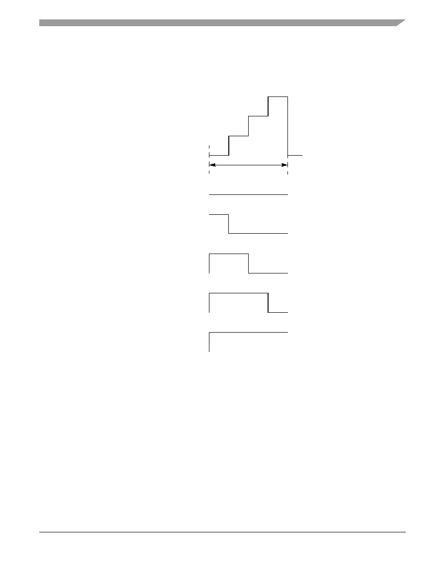
Timebase
MC68HC908LB8 Data Sheet, Rev. 0
Freescale Semiconductor
143
in
Figure 15-4
. Again, the timer modulus register is used to determine the maximum count. The PWM
period will equal:
(timer modulus) x (PWM clock period)
Figure 15-4. Edge-Aligned PWM (Positive Polarity)
15.3.2 Prescaler
To permit lower PWM frequencies, a prescaler is provided which will divide the PWM clock frequency by
1, 2, 4, or 8.
Table 15-1
shows how setting the prescaler bits in PWM control register 2 affects the PWM
clock frequency. This prescaler is buffered and will not be used by the PWM generator until the LDOK bit
is set and a new PWM reload cycle begins.
UP-ONLY COUNTER
MODULUS = 4
PWM = 0
PWM = 1
PWM = 2
PWM = 3
PWM = 4
PERIOD = 4 X (PWM
CLOCK PERIOD)

Pulse Width Modulator with Fault Input (PWM)
MC68HC908LB8 Data Sheet, Rev. 0
144
Freescale Semiconductor
15.4 PWM Generators
Pulse-width modulator (PWM) generators are discussed in this subsection.
15.4.1 Load Operation
To help avoid erroneous pulse widths and PWM periods, the modulus, prescaler, and PWM value
registers are buffered. New PWM values, counter modulus values, and prescalers can be loaded from
their buffers into the PWM module every one, two, four, or eight PWM cycles. LDFQ1 and LDFQ0 in PWM
control register 2 are used to control this reload frequency, as shown in
Table 15-2
. When a reload cycle
arrives, regardless of whether an actual reload occurs (as determined by the LDOK bit), the PWM reload
flag bit in PWM control register 1 will be set. If the PWMINT bit in PWM control register 1 is set, a CPU
interrupt request will be generated when PWMF is set. Software can use this interrupt to calculate new
PWM parameters in real time for the PWM module.
Table 15-1. PWM Prescaler
Prescaler Bits
PRSC1 and PRSC0
PWM Clock Frequency
00
BUSCLK
01
BUSCLK/2
10
BUSCLK/4
11
BUSCLK/8
Table 15-2. PWM Reload Frequency
Reload Frequency Bits
LDFQ1 and LDFQ0
PWM Reload Frequency
00
Every PWM cycle
01
Every 2 PWM cycles
10
Every 4 PWM cycles
11
Every 8 PWM cycles

PWM Generators
MC68HC908LB8 Data Sheet, Rev. 0
Freescale Semiconductor
145
For ease of software, the LDFQx bits are buffered. When the LDFQx bits are changed, the reload
frequency will not change until the previous reload cycle is completed. See
Figure 15-5
.
NOTE
When reading the LDFQx bits, the value is the buffered value (for example,
not necessarily the value being acted upon).
Figure 15-5. Reload Frequency Change
PWMINT enables CPU interrupt requests as shown in
Figure 15-6
. When this bit is set, CPU interrupt
requests are generated when the PWMF bit is set. When the PWMINT bit is clear, PWM interrupt requests
are inhibited. PWM reloads will still occur at the reload rate, but no interrupt requests will be generated.
Figure 15-6. PWM Interrupt Requests
To prevent a partial reload of PWM parameters from occurring while the software is still calculating them,
an interlock bit controlled from software is provided. This bit informs the PWM module that all the PWM
parameters have been calculated, and it is "okay" to use them. A new modulus, prescaler, and/or PWM
value cannot be loaded into the PWM module until the LDOK bit in PWM control register 1 is set. When
the LDOK bit is set, these new values are loaded into a second set of registers and used by the PWM
generator at the beginning of the next PWM reload cycle as shown in
Figure 15-7
and
Figure 15-8
. After
these values are loaded, the LDOK bit is cleared.
NOTE
When the PWM module is enabled (via the PWMEN bit), a load will occur
if the LDOK bit is set. Even if it is not set, an interrupt will occur if the
PWMINT bit is set. To prevent this, the software should clear the PWMINT
bit before enabling the PWM module.
NOTE
Setting PWMEN forces PWM1 and PWM0 to be inputs and the
appropriately configured FAULT pin to be an output, overriding the data
RELOAD
RELOAD
RELOAD
RELOAD
RELOAD
RELOAD
RELOAD
CHANGE RELOAD
FREQUENCY TO
EVERY 4 CYCLES
CHANGE RELOAD
FREQUENCY TO
EVERY CYCLE
LATCH
V
DD
CPU INTERRUPT
RESET
D
CK
PWMINT
PWMF
PWM RELOAD
READ PWMF AS 1,
WRITE PWMF AS 0
OR RESET
REQUEST

Pulse Width Modulator with Fault Input (PWM)
MC68HC908LB8 Data Sheet, Rev. 0
146
Freescale Semiconductor
direction register. In order to read the states of the pins, the data direction
register bit must be a 0.
Figure 15-7. Edge-Aligned PWM Value Loading
Figure 15-8. Edge-Aligned Modulus Loading
15.4.2 PWM Data Overflow and Underflow Conditions
The PWM value registers are 16-bit registers. Although the counter is only 12 bits, the user may write a
16-bit signed value to a PWM value register. As shown in
Figure 15-4
, if the PWM value is less than or
equal to zero, the PWM will be inactive for the entire period. Conversely, if the PWM value is greater than
or equal to the timer modulus, the PWM will be active for the entire period. Refer to
Table 15-3
.
LDOK = 1
MODULUS = 3
PWM VALUE = 1
LDOK = 1
MODULUS = 3
PWM VALUE = 2
UP-ONLY
COUNTER
PWM
LDFQ1:LDFQ0 = 00 (RELOAD EVERY CYCLE)
LDOK = 0
MODULUS = 3
PWM VALUE = 2
LDOK = 0
MODULUS = 3
PWM VALUE = 1
LDOK = 0
MODULUS = 3
PWM VALUE = 1
PWMF SET
PWMF SET
PWMF SET
PWMF SET
PWMF SET
LDOK = 1
MODULUS = 3
PWM VALUE = 2
LDOK = 1
MODULUS = 4
PWM VALUE = 2
LDOK = 1
MODULUS = 2
PWM VALUE = 2
UP-ONLY
COUNTER
PWM
LDFQ1:LDFQ0 = 00 (RELOAD EVERY CYCLE)
LDOK = 0
MODULUS = 1
PWM VALUE = 2
PWMF SET
PWMF SET
PWMF SET
PWMF SET

Fault Protection
MC68HC908LB8 Data Sheet, Rev. 0
Freescale Semiconductor
147
NOTE
The terms "active" and "inactive" refer to the asserted and negated states
of the PWM signals and should not be confused with the high-impedance
state of the PWM pins.
15.4.3 Output Polarity
The output polarity of the PWMs is determined by the POLx bits. Positive polarity means that when the
PWM is active, the PWM output is high. Conversely, negative polarity means that when the PWM is
active, PWM output is low. See
Figure 15-9
.
Figure 15-9. PWM Output Polarity
15.5 Fault Protection
Conditions may arise in the external drive circuitry which require that the PWM signals become inactive
immediately. Furthermore, it may be desirable to selectively disable PWM(s) solely with software.
One or more PWM pins can be disabled (forced to their inactive state) by applying a logic high to the
external fault pin or by writing a logic high to either of the disable bits (DIS0 and DIS1 in PWM control
register 1).
Figure 15-10
shows the structure of the PWM disabling scheme. While the PWM pins are
disabled, they are forced to their inactive state. The PWM generator continues
A fault can also generate a CPU interrupt. The fault pin has its own interrupt vector.
15.5.1 Fault Condition Input Pin
A logic high level on a fault pin disables the PWM(s) determined by the disable map bits (MAPx). The
external fault pin is software-configurable to re-enable the PWMs either with the fault pin (automatic
Table 15-3. PWM Data Overflow and Underflow Conditions
PWMVALxH:PWMVALxL
Condition
PWM Value Used
$0000≠$0FFF
Normal
Per register contents
$1000≠$7FFF
Overflow
$FFF
$8000≠$FFFF
Underflow
$000
UP-ONLY COUNTER
MODULUS = 4
PWM <= 0
PWM = 1
PWM = 2
PWM = 3
PWM >= 4
EDGE-ALIGNED POSITIVE POLARITY
MODULUS = 4
PWM <= 0
PWM = 1
PWM = 2
PWM = 3
PWM >= 4
EDGE-ALIGNED NEGATIVE POLARITY

Pulse Width Modulator with Fault Input (PWM)
MC68HC908LB8 Data Sheet, Rev. 0
148
Freescale Semiconductor
mode) or with software (manual mode). The fault pin has an associated FMODE bit to control the PWM
re-enabling method. Automatic mode is selected by setting the FMODE bit in the fault control register.
Manual mode is selected when FMODE is clear.
The operation of the fault pin is asnynchronous. If it is enabled by either the MAP0 or MAP1 disable bits
and the fault pin goes high, the associated PWM(s) outputs are immediately disabled without waiting for
the next bus cycle.
The location of the fault pin is software configurable to one of two locations. Enabling the fault functionality
of a given pin does not disconnect that pin from any other module that is trying to use the pin.
Figure 15-10. PWM Disabling Scheme
15.5.1.1 Automatic Mode
In automatic mode, the PWM(s) are disabled immediately once a fault condition is detected (logic high).
The PWM(s) remain disabled until the fault condition is cleared (logic low) and a new PWM cycle begins
as shown in
Figure 15-11
. Clearing the FFLAG event bit will not enable the PWMs in automatic mode.
Figure 15-11. PWM Disabling in Automatic Mode
The fault pin's logic state is reflected in the FPIN bit. Any write to this bit is overwritten by the pin state.
The FFLAG event bit is set with each rising edge of the fault pin. To clear the FFLAG bit, the user must
write a 1 to the FTACK bit.
FAULT
PIN1
FINT1
CYCLE START
LOGIC HIGH FOR FAULT
PWM DISABLE
FMODE
CLEAR BY WRITING 1 TO FTACK
INTERRUPT REQUEST
SHOT
S
Q
R
S
Q
R
ONE
FFLAG
MANUAL
MODE
AUTO
MODE
FAULT PIN DISABLE
Note:
In manual mode (FMODE = 0), fault may be cleared only if a logic level low at the input of the fault pin is present.
PWM(S) ENABLED
PWM(S) ENABLED
PWM(S) DISABLED (INACTIVE)
FAULT PIN

Fault Protection
MC68HC908LB8 Data Sheet, Rev. 0
Freescale Semiconductor
149
If the FINT bit is set, a fault condition resulting in setting the FFLAG bit will also latch a CPU interrupt
request. The interrupt request latch is not cleared until one of these actions occurs:
∑
The FFLAG bit is cleared by writing a 1 to the corresponding FTACK bit.
∑
The FINT bit is cleared. This will not clear the FFLAG bit.
∑
A reset automatically clears the interrupt latch.
If prior to a vector fetch, the interrupt request latch is cleared by one of the actions listed, a CPU interrupt
will no longer be requested. A vector fetch does not alter the state of the PWMs, the FFLAG event flag,
or FINT.
NOTE
If the FFLAG or FINT bits are not cleared during the interrupt service
routine, the interrupt request latch will not be cleared.
15.5.1.2 Manual Mode
In manual mode, the PWM(s) are disabled immediately once a fault condition is detected (logic high). The
PWM(s) remain disabled until software clears the FFLAG event bit and a new PWM cycle begins. A fault
condition on the pin can only be cleared, allowing the PWM(s) to enable, if a logic low level at the fault pin
is present at the start of a PWM cycle. See
Figure 15-12
.
The function of the fault control and event bits is the same as in automatic mode except that the PWMs
are not re-enabled until the FFLAG event bit is cleared by writing to the FTACK bit and the fault condition
is cleared (logic low).
Figure 15-12. PWM Disabling in Manual Mode
15.5.2 Software Output Disable
Setting PWM disable bit DIS0 or DIS1 in PWM control register 1 immediately disables the corresponding
PWM pins. The PWM pin(s) remain disabled until the PWM disable bit is cleared and a new PWM cycle
begins as shown in
Figure 15-13
. Setting a PWM disable bit does not latch a CPU interrupt request, and there are no event
flags associated with the PWM disable bits.
PWM(S) ENABLED
PWM(S) ENABLED
PWM(S) DISABLED
FFLAGX CLEARED
FAULT PIN 2 OR 4

Pulse Width Modulator with Fault Input (PWM)
MC68HC908LB8 Data Sheet, Rev. 0
150
Freescale Semiconductor
15.6 Initialization and the PWMEN Bit
For proper operation, all registers should be initialized and the LDOK bit should be set before enabling
the PWM via the PWMEN bit. When the PWMEN bit is first set, a reload will occur immediately, setting
the PWMF flag and generating an interrupt if PWMINT is set.
NOTE
If the LDOK bit is not set when PWMEN is set after a RESET, the prescaler
and PWM values will be 0, but the modulus will be unknown. If the LDOK
bit is not set after the PWMEN bit has been cleared then set (without a
RESET), the modulus value that was last loaded will be used.
Because of the equals-comparator architecture of this PWM, the modulus =
0 case is considered illegal. Therefore, the modulus register is not reset,
and a modulus value of 0 will result in waveforms inconsistent with the other
modulus waveforms. See
15.8.2 PWM Counter Modulo Registers
.
When PWMEN is set, the PWM pins change from high impedance to outputs. At this time, assuming no
fault condition is present, the PWM pins will drive according to the PWM values and polarity. See the
timing diagram in
Figure 15-13
.
Figure 15-13. PWMEN and PWM Pins
When the PWMEN bit is cleared, this will occur:
∑
PWM pins will be three-stated
∑
PWM counter is cleared and will not be clocked
∑
Internally, the PWM generator will force its outputs to 0 to avoid glitches when the PWMEN is set
again
When PWMEN is cleared, all fault circuitry remains active.
NOTE
The PWMF flag and pending CPU interrupts are NOT cleared when
PWMEN = 0.
15.7 PWM Operation in Low-Power Modes
15.7.1 Wait Mode
When the microcontroller is put in low-power wait mode via the WAIT instruction, all clocks to the PWM
module will continue to run. If an interrupt is issued from the PWM module (via a reload or a fault), the
microcontroller will exit wait mode.
CPU CLOCK
PWMEN
PWM PINS
DRIVE ACCORDING TO PWM
VALUE AND POLARITY
PORT FUNCTION
PORT FUNCTION

Control Logic Block
MC68HC908LB8 Data Sheet, Rev. 0
Freescale Semiconductor
151
Clearing the PWMEN bit before entering wait mode will reduce power consumption in wait mode because
the counter, prescaler divider, and LDFQ divider will no longer be clocked. In addition, power will be
reduced because the PWMs will no longer toggle.
15.7.2 Stop Mode
When the microcontroller is put into stop mode via the STOP instruction, the PWM will stop functioning.
The PWM0 and PWM1 outputs are set to logic 0. The STOP instruction does not affect the register
conditions or the state of the PWM counters. When the MCU exits stop mode after an external interrupt
the PWM resumes operation.
15.8 Control Logic Block
This subsection provides a description of the control logic block.
15.8.1 PWM Counter Registers
The PWM counter registers (PCNTH and PCNTL) display the 12-bit up-only counter. When the high byte
of the counter is read, the lower byte is latched. PCNTL will hold this latched value until it is read. See
Figure 15-14
and
Figure 15-15
.
15.8.2 PWM Counter Modulo Registers
The PWM counter modulus registers (PMODH and PMODL) hold a 12-bit unsigned number that
determines the maximum count for the up-only counter. The PWM period will equal the modulus. See
Figure 15-16
and
Figure 15-17
.
Address:
$0045
Bit 7
6
5
4
3
2
1
Bit 0
Read:
0
0
0
0
Bit 11
Bit 10
Bit 9
Bit 8
Write:
Reset:
0
0
0
0
0
0
0
0
= Unimplemented
Figure 15-14. PWM Counter Register High (PCNTH)
Address:
$0046
Bit 7
6
5
4
3
2
1
Bit 0
Read:
Bit 7
Bit 6
Bit 5
Bit 4
Bit 3
Bit 2
Bit 1
Bit 0
Write:
Reset:
0
0
0
0
0
0
0
0
= Unimplemented
Figure 15-15. PWM Counter Register Low (PCNTL)

Pulse Width Modulator with Fault Input (PWM)
MC68HC908LB8 Data Sheet, Rev. 0
152
Freescale Semiconductor
To avoid erroneous PWM periods, this value is buffered and will not be used by the PWM generator until
the LDOK bit has been set and the next PWM load cycle begins.
NOTE
When reading this register, the value read is the buffer (not necessarily the
value the PWM generator is currently using).
Because of the equals-comparator architecture of this PWM, the modulus =
0 case is considered illegal. Therefore, the modulus register is not reset,
and a modulus value of 0 will result in waveforms inconsistent with the other
modulus waveforms. If a modulus of 0 is loaded, the counter will continually
count down from $FFF. This operation will not be tested or guaranteed (the
user should consider it illegal). However, the fault conditions will still be
guaranteed.
15.8.3 PWMx Value Registers
Each of the two PWMs has a 16-bit PWM value register.
Address:
$0047
Bit 7
6
5
4
3
2
1
Bit 0
Read:
0
0
0
0
Bit 11
Bit 10
Bit 9
Bit 8
Write:
Reset:
0
0
0
0
Indeterminate after reset
= Unimplemented
Figure 15-16. PWM Counter Modulo Register High (PMODH)
Address:
$0048
Bit 7
6
5
4
3
2
1
Bit 0
Read:
Bit 7
Bit 6
Bit 5
Bit 4
Bit 3
Bit 2
Bit 1
Bit 0
Write:
Reset:
Indeterminate after reset
Figure 15-17. PWM Counter Modulo Register Low (PMODL)
Bit 7
6
5
4
3
2
1
Bit 0
Read:
Bit 15
Bit 14
Bit 13
Bit 12
Bit 11
Bit 10
Bit 9
Bit 8
Write:
Reset:
0
0
0
0
0
0
0
0
Bold
= Buffered
Figure 15-18. PWMx Value Registers High (PVALxH)

Control Logic Block
MC68HC908LB8 Data Sheet, Rev. 0
Freescale Semiconductor
153
The 16-bit signed value stored in this register determines the duty cycle of the PWM. The duty cycle is
defined as:
(PWM value/modulus) x 100
Writing a number less than or equal to 0 causes the PWM to be off for the entire PWM period. Writing a
number greater than or equal to the 12-bit modulus causes the PWM to be on for the entire PWM period.
To avoid erroneous PWM pulses, this value is buffered and will not be used by the PWM generator until
the LDOK bit has been set and the next PWM load cycle begins.
NOTE
When reading these registers, the value read is the buffer (not necessarily
the value the PWM generator is currently using).
15.8.4 PWM Control Register 1
PWM control register 1 (PCTL1) controls PWM enabling/disabling, the location of the PWM Fault bit, the
loading of new modulus, prescaler, PWM values, and the PWM correction method.
FPOS -- Fault Pin Position Bit
This read/write bit allows the user to select the location of the Fault pin.
1 = Fault pin functionality is placed on PTB2
0 = Fault pin functionality is placed on PTB7
NOTE
Placing the Fault pin on PTB7 will not affect the ADC or the op
amp/comparator connections. This is to allow the output of the op
amp/comparator to be used as the input to the Fault pin and for this same
signal to be simultaneously measured by the ADC.
PWMINT -- PWM Interrupt Enable Bit
This read/write bit allows the user to enable and disable PWM CPU interrupts. If set, a CPU interrupt
will be pending when the PWMF flag is set.
1 = Enable PWM CPU interrupts
0 = Disable PWM CPU interrupts
Bit 7
6
5
4
3
2
1
Bit 0
Read:
Bit 7
Bit 6
Bit 5
Bit 4
Bit 3
Bit 2
Bit 1
Bit 0
Write:
Reset:
0
0
0
0
0
0
0
0
Bold
= Buffered
Figure 15-19. PWMx Value Registers Low (PVALxL)
Address:
$0040
Bit 7
6
5
4
3
2
1
Bit 0
Read:
0
FPOS
PWMINT
PWMF
0
0
LDOK
PWMEN
Write:
Reset:
0
0
0
0
0
0
0
0
= Unimplemented
Figure 15-20. PWM Control Register 1 (PCTL1)

Pulse Width Modulator with Fault Input (PWM)
MC68HC908LB8 Data Sheet, Rev. 0
154
Freescale Semiconductor
NOTE
When PWMINT is cleared, pending CPU interrupts are inhibited.
PWMF -- PWM Reload Flag
This read/write bit is set at the beginning of every reload cycle regardless of the state of the LDOK bit.
This bit is cleared by reading PWM control register 1 with the PWMF flag set, then writing a 0 to PWMF.
If another reload occurs before the clearing sequence is complete, then writing 0 to PWMF has no
effect.
1 = New reload cycle began
0 = New reload cycle has not begun
NOTE
When PWMF is cleared, pending PWM CPU interrupts are cleared (not
including fault interrupts).
LDOK-- Load OK Bit
This read/write bit loads the prescaler bits of the PMCTL2 register and the entire PMMODH/L and
PWMVALH/L registers into a set of buffers. The buffered prescaler divisor, PWM counter modulus
value, and PWM pulse will take effect at the next PWM load. Set LDOK by reading it when it is 0 and
then writing a 1 to it. LDOK is automatically cleared after the new values are loaded or can be manually
cleared before a reload by writing a 0 to it. Reset clears LDOK.
1 = Load prescaler, modulus, and PWM values
0 = Do not load new modulus, prescaler, and PWM values
NOTE
The user should initialize the PWM registers and set the LDOK bit before
enabling the PWM. A PWM CPU interrupt request can still be generated
when LDOK is 0.
PWMEN -- PWM Module Enable Bit
This read/write bit enables and disables the PWM generator and the PWM pins. When PWMEN is
clear, the PWM generator is disabled and the PWM pins are in the high-impedance state.
When the PWMEN bit is set, the PWM generator and PWM pins are activated.
For more information, see
15.6 Initialization and the PWMEN Bit
.
1 = PWM generator and PWM pins enabled
0 = PWM generator and PWM pins disabled
15.8.5 PWM Control Register 2
PWM control register 2 (PCTL2) controls the PWM load frequency, PWM channel enabling/disabling, the
PWM polarity, the PWM correction method, and the PWM counter prescaler. For ease of software and to
avoid erroneous PWM periods, some of these register bits are buffered. The PWM generator will not use
the prescaler value until the LDOK bit has been set, and a new PWM cycle is starting. The load frequency
bits are not used until the current load cycle is complete.
See
Figure 15-21
.
NOTE
The user should initialize this register before enabling the PWM.

Control Logic Block
MC68HC908LB8 Data Sheet, Rev. 0
Freescale Semiconductor
155
LDFQ1 and LDFQ0 -- PWM Load Frequency Bits
These buffered read/write bits select the PWM CPU load frequency according to
Table 15-4
.
NOTE
When reading these bits, the value read is the buffer value (not necessarily
the value the PWM generator is currently using).
The LDFQx bits take effect when the current load cycle is complete
regardless of the state of the load okay bit, LDOK.
NOTE
Reading the LDFQx bit reads the buffered values and not necessarily the
values currently in effect.
DIS1 -- Software Disable Bit for PWM1
This read/write bit allows the user to disable pin PWM1.
1 = Disable PWM1
0 = Re-enable PWM1
DIS0 -- Software Disable Bit for PWM0
This read/write bit allows the user to disable pin PWM0.
1 = Disable PWM0
0 = Re-enable PWM0
POL1 -- Polarity Bit for PWM1
This read/write bit selects the polarity of the PWM waveform of PWM1. Positive polarity means that
when the PWM is active the PWM output is high. Conversely, negative polarity means that when the
PWM is active the PWM output is low.
1 = PWM1 has positive polarity
0 = PWM1 has negative polarity
Address:
$0041
Bit 7
6
5
4
3
2
1
Bit 0
Read:
LDFQ1
LDFQ0
DIS1
DIS0
POL1
POL0
PRSC1
PRSC0
Write:
Reset:
0
0
0
0
1
1
0
0
Bold
= Buffered
Figure 15-21. PWM Control Register 2 (PCTL2)
Table 15-4. PWM Reload Frequency
Reload Frequency Bits
LDFQ1 and LDFQ0
PWM Reload
Frequency
00
Every PWM cycle
01
Every 2 PWM cycles
10
Every 4 PWM cycles
11
Every 8 PWM cycles

Pulse Width Modulator with Fault Input (PWM)
MC68HC908LB8 Data Sheet, Rev. 0
156
Freescale Semiconductor
POL0 -- This read/write bit selects the polarity of the PWM waveform of PWM1. Positive polarity
means that when the PWM is active the PWM output is high. Conversely, negative polarity means that
when the PWM is active the PWM output is low.
1 = PWM0 has positive polarity
0 = PWM0 has negative polarity
PRSC1 and PRSC0 -- PWM Prescaler Bits
These buffered read/write bits allow the PWM clock frequency to be modified as shown in
Table 15-5
.
NOTE
When reading these bits, the value read is the buffer value (not necessarily
the value the PWM generator is currently using).
15.8.6 PWM Disable Mapping Write-Once Register
The PWM disable mapping write-once register (DISMAP) contains two bits that control the PWM pins that
will be disabled if an external fault occurs. After this register is written for the first time, it cannot be
rewritten unless a reset occurs.
MAP1 -- Disable Map for PWM1 Bit
This write-once bit allows the user to select PWM1 to be disabled when a logic 1 is present on the
FAULT pin.
1 = Disables PWM1 when an external fault occurs
0 = Prevents PWM1 from being disabled by hardware
MAP0 -- Disable Map for PWM0 Bit
This write-once bit allows the user to select PWM0 to be disabled when a logic 1 is present on the
FAULT pin.
1 = Disables PWM0 when an external fault occurs
0 = Prevents PWM0 from being disabled by hardware
Table 15-5. PWM Prescaler
Prescaler Bits
PRSC1 and PRSC0
PWM Clock
Frequency
00
BUSCLK
01
BUSCLK/2
10
BUSCLK/4
11
BUSCLK/8
Address:
$004D
Bit 7
6
5
4
3
2
1
Bit 0
Read:
0
0
0
0
0
0
MAP1
MAP0
Write:
Reset:
0
0
0
0
0
0
1
1
= Unimplemented
Figure 15-22. PWM Disable Mapping Write-Once Register (DISMAP)

Control Logic Block
MC68HC908LB8 Data Sheet, Rev. 0
Freescale Semiconductor
157
15.8.7 Fault Control Register
The fault control register (FCR) controls the fault-protection circuitry.
FINT -- Fault Interrupt Enable Bit
This read/write bit allows the CPU interrupt caused by faults on the fault pin to be enabled. The fault
protection circuitry is independent of this bit and will always be active. If a fault is detected, the PWM
pins will still be disabled according to the disable mapping register.
1 = Fault pin will cause CPU interrupts
0 = Fault pin will not cause CPU interrupts
FMODE -- Fault Mode Selection for Fault Pin Bit (automatic versus manual mode)
This read/write bit allows the user to select between automatic and manual mode faults. For further
descriptions of each mode, see
15.5 Fault Protection
.
1 = Automatic mode
0 = Manual mode
15.8.8 Fault Status Register
The fault status register (FSR) is a read-only register that indicates the current fault status.
FPIN -- State of Fault Pin Bit
This read-only bit allows the user to read the current state of the fault pin.
1 = Fault pin is at logic 1
0 = Fault pin is at logic 0
FFLAG -- Fault Event Flag
The FFLAG event bit is set immediately when a rising edge is seen on the fault pin. To clear the FFLAG
bit, the user must write a 1 to the FTACK bit in the fault acknowledge register.
1 = A fault has occurred on the fault pin
0 = No new fault on the fault pin
Address: $0042
Bit 7
6
5
4
3
2
1
Bit 0
Read:
0
0
0
0
0
0
FINT
FMODE
Write:
Reset:
0
0
0
0
0
0
0
0
= Unimplemented
Figure 15-23. Fault Control Register (FCR)
Address:
$0043
Bit 7
6
5
4
3
2
1
Bit 0
Read:
0
0
0
0
0
0
FPIN
FFLAG
Write:
Reset:
0
0
0
0
0
0
U
0
= Unimplemented
U = Unaffected
Figure 15-24. Fault Status Register (FSR)

Pulse Width Modulator with Fault Input (PWM)
MC68HC908LB8 Data Sheet, Rev. 0
158
Freescale Semiconductor
15.8.9 Fault Control Register 2
The fault control register 2 (FCR2) is used to acknowledge and clear the FFLAG.
FTACK -- Fault Acknowledge Bit
The FTACK bit is used to acknowledge and clear FFLAG. This bit will always read 0. Writing a 1 to this
bit will clear FFLAG. Writing a 0 will have no effect.
15.9 PWM Glossary
CPU cycle
One internal bus cycle (1/BUSCLK)
PWM clock cycle (or period)
One tick of the PWM counter (1/BUSCLK with no prescaler). See
Figure 15-26
.
PWM cycle (or period)
Edge-aligned mode: The time it takes the PWM counter to count up (modulus/BUSCLK). See
Figure 15-26
.
Figure 15-26. PWM Clock Cycle and PWM Cycle Definition
Address: $0044
Bit 7
6
5
4
3
2
1
Bit 0
Read:
0
0
0
0
0
0
0
0
Write:
FTACK
Reset:
0
0
0
0
0
0
0
0
= Unimplemented
Figure 15-25. Fault Control Register (FCR2)
PWM
PWM CYCLE (OR PERIOD)
CLOCK
CYCLE
Edge-Aligned Mode

PWM Glossary
MC68HC908LB8 Data Sheet, Rev. 0
Freescale Semiconductor
159
PWM Load Frequency
Frequency at which new PWM parameters get loaded into the PWM. See
Figure 15-27
.
Figure 15-27. PWM Load Cycle/Frequency Definition
RELOAD NEW
MODULUS,
PRESCALER, &
PWM VALUES IF
LDOK = 1
RELOAD NEW
MODULUS,
PRESCALER, &
PWM VALUES
IF LDOK = 1
PWM LOAD CYCLE
LDFQ1:LDFQ0 = 01 -- Reload Every Two Cycles
(1/PWM LOAD FREQUENCY)

Pulse Width Modulator with Fault Input (PWM)
MC68HC908LB8 Data Sheet, Rev. 0
160
Freescale Semiconductor

MC68HC908LB8 Data Sheet, Rev. 0
Freescale Semiconductor
161
Chapter 16
Resets and Interrupts
16.1 Introduction
Resets and interrupts are responses to exceptional events during program execution. A reset re-initializes
the microcontroller (MCU) to its startup condition. An interrupt vectors the program counter to a service
routine.
16.2 Resets
A reset immediately returns the MCU to a known startup condition and begins program execution from a
user-defined memory location.
16.2.1 Effects
A reset:
∑
Immediately stops the operation of the instruction being executed
∑
Initializes certain control and status bits
∑
Loads the program counter with a user-defined reset vector address from locations $FFFF and
$FFFE
16.2.2 External Reset
A logic 0 applied to RST for a time, t
IRL
, generates an external reset when pin PTA5/RST/KB5 is
configured as a reset pin. An external reset sets the PIN bit in the system integration module (SIM) reset
status register.
16.2.3 Internal Reset
Sources:
∑
Power-on reset (POR)
∑
Computer operating properly (COP)
∑
Low-power reset circuits
∑
Illegal opcode
∑
Illegal address
16.2.3.1 Power-On Reset (POR)
A power-on reset (POR) is an internal reset caused by a positive transition on the V
DD
pin. V
DD
at the
POR must go below POR rearm voltage (V
POR
) to reset the MCU. This distinguishes between a reset and
a POR. The POR is not a brown-out detector, low-voltage detector, or glitch detector.
A power-on reset:
∑
Drives the RST pin low during the oscillator stabilization delay

Resets and Interrupts
MC68HC908LB8 Data Sheet, Rev. 0
162
Freescale Semiconductor
∑
Releases the RST pin 32 BUSCLKX4 cycles after the oscillator stabilization delay
∑
Sets the POR bit in the SIM reset status register and clears all other bits in the register
Figure 16-1. Power-On Reset Recovery
16.2.3.2 Computer Operating Properly (COP) Reset
A computer operating properly (COP) reset is an internal reset caused by an overflow of the COP counter.
A COP reset sets the COP bit in the SIM reset status register.
To clear the COP counter and prevent a COP reset, write any value to the COP control register at location
$FFFF.
16.2.3.3 Low-Voltage Inhibit (LVI) Reset
A low-voltage inhibit (LVI) reset is an internal reset caused by a drop in the power supply voltage to the
LVI
TRIPF
voltage.
An LVI reset:
∑
Holds the clocks to the CPU and modules inactive for an oscillator stabilization delay of 4096
BUSCLKX4 cycles after the power supply voltage rises to the LVI
TRIPF
voltage
∑
Drives the RST pin low for as long as V
DD
is below the LVI
TRIPF
voltage and during the oscillator
stabilization delay
∑
Sets the LVI bit in the SIM reset status register
16.2.3.4 Illegal Opcode Reset
An illegal opcode reset is an internal reset caused by an opcode that is not in the instruction set. An illegal
opcode reset sets the ILOP bit in the SIM reset status register.
If the stop enable bit, STOP, in the CONFIG1 register is a 0, the STOP instruction causes an illegal
opcode reset.
16.2.3.5 Illegal Address Reset
An illegal address reset is an internal reset caused by opcode fetch from an unmapped address. An illegal
address reset sets the ILAD bit in the SIM reset status register.
A data fetch from an unmapped address does not generate a reset.
PORRST
(1)
OSC1
BUSCLKX4
BUSCLKX2
RST PIN
4096
CYCLES
32
CYCLES
1. PORRST is an internally generated power-on reset pulse.

Resets
MC68HC908LB8 Data Sheet, Rev. 0
Freescale Semiconductor
163
16.2.4 System Integration Module (SIM) Reset Status Register
This read-only register contains flags to show reset sources. All flag bits are automatically cleared
following a read of the register. Reset service can read the SIM reset status register to clear the register
after power-on reset and to determine the source of any subsequent reset.
The register is initialized on power-up as shown with the POR bit set and all other bits cleared. During a
POR or any other internal reset, the RST pin is pulled low as long as pin PTA5/RST/KB5 is configured for
reset operation.
NOTE
Only a read of the SIM reset status register clears all reset flags. After
multiple resets from different sources without reading the register, multiple
flags remain set.
POR -- Power-On Reset Flag
1 = Power-on reset since last read of SRSR
0 = Read of SRSR since last power-on reset
PIN -- External Reset Flag
1 = External reset via RST pin since last read of SRSR
0 = POR or read of SRSR since last external reset
COP -- Computer Operating Properly Reset Bit
1 = Last reset caused by timeout of COP counter
0 = POR or read of SRSR since any reset
ILOP -- Illegal Opcode Reset Bit
1 = Last reset caused by an illegal opcode
0 = POR or read of SRSR since any reset
ILAD -- Illegal Address Reset Bit
1 = Last reset caused by an opcode fetch from an illegal address
0 = POR or read of SRSR since any reset
MODRST -- Monitor Mode Entry Module Reset Bit
1 = Last reset caused by forced monitor mode entry.
0 = POR or read of SRSR since any reset
LVI -- Low-Voltage Inhibit Reset Bit
1 = Last reset caused by low-power supply voltage
0 = POR or read of SRSR since any reset
Address:
$FE01
Bit 7
6
5
4
3
2
1
Bit 0
Read:
POR
PIN
COP
ILOP
ILAD
MODRST
LVI
0
Write:
POR:
1
0
0
0
0
0
0
0
= Unimplemented
Figure 16-2. SIM Reset Status Register (SRSR)
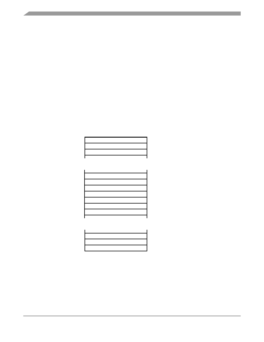
Resets and Interrupts
MC68HC908LB8 Data Sheet, Rev. 0
164
Freescale Semiconductor
16.3 Interrupts
An interrupt temporarily changes the sequence of program execution to respond to a particular event. An
interrupt does not stop the operation of the instruction being executed, but begins when the current
instruction completes its operation.
16.3.1 Effects
An interrupt:
∑
Saves the CPU registers on the stack. At the end of the interrupt, the RTI instruction recovers the
CPU registers from the stack so that normal processing can resume.
∑
Sets the interrupt mask (I bit) to prevent additional interrupts. Once an interrupt is latched, no other
interrupt can take precedence, regardless of its priority.
∑
Loads the program counter with a user-defined vector address
After every instruction, the CPU checks all pending interrupts if the I bit is not set. If more than one
interrupt is pending when an instruction is done, the highest priority interrupt is serviced first. In the
example shown in
Figure 16-4
, if an interrupt is pending upon exit from the interrupt service routine, the
pending interrupt is serviced before the LDA instruction is executed.
Figure 16-3. Interrupt Stacking Order
CONDITION CODE REGISTER
ACCUMULATOR
INDEX REGISTER (LOW BYTE)
(1)
PROGRAM COUNTER (HIGH BYTE)
PROGRAM COUNTER (LOW BYTE)
∑
∑
∑
∑
∑
∑
1
2
3
4
5
5
4
3
2
1
STACKING
ORDER
1. High byte of index register is not stacked.
$00FF DEFAULT ADDRESS ON RESET
UNSTACKING
ORDER

Interrupts
MC68HC908LB8 Data Sheet, Rev. 0
Freescale Semiconductor
165
Figure 16-4
.
Interrupt Recognition Example
The LDA opcode is prefetched by both the INT1 and INT2 RTI instructions. However, in the case of the
INT1 RTI prefetch, this is a redundant operation.
NOTE
To maintain compatibility with the M6805 Family, the H register is not
pushed on the stack during interrupt entry. If the interrupt service routine
modifies the H register or uses the indexed addressing mode, save the H
register and then restore it prior to exiting the routine.
See
Figure 16-5
for a flowchart depicting interrupt processing.
16.3.2 Sources
The sources in
Table 16-1
can generate CPU interrupt requests.
CLI
LDA
INT1
PULH
RTI
INT2
BACKGROUND
#$FF
PSHH
INT1 INTERRUPT SERVICE ROUTINE
PULH
RTI
PSHH
INT2 INTERRUPT SERVICE ROUTINE
ROUTINE

Resets and Interrupts
MC68HC908LB8 Data Sheet, Rev. 0
166
Freescale Semiconductor
Table 16-1. Interrupt Sources
Source
Flag
Mask
(1)
NOTES:
1. The I bit in the condition code register is a global mask for all interrupt sources except the SWI
instruction.
Priority
(2)
2. 0 = highest priority
Vector
Address
Reset
None
None
0
$FFFF≠$FFFE
SWI instruction
None
None
1
$FFFD≠$FFFC
IRQ pin
IRQF
IMASK
2
$FFFA≠$FFFB
TIM channel 0
CH0F
CH0IE
3
$FFF7≠$FFF6
TIM channel 1
CH1F
CH1IE
4
$FFF5≠$FFF4
TIM overflow
TOF
TOIE
5
$FFF3≠$FFF2
FAULT interrupt (PWM)
FFLAG
FINT
6
$FFF1≠$FFF0
PWMINT interrupt (PWM)
PWMINT
WPMF
7
$FFEF≠$FFEE
SHTDWN interrupt
SHTIF
SHTIEN
8
$FFED≠$FFEC
Keyboard pin
KEYF
IMASKK
9
$FFE1≠$FFE0
ADC conversion complete
COCO
AIEN
10
$FFDF-$FFDE
Interrupts
MC68HC908LB8 Data Sheet, Rev. 0
Freescale Semiconductor
167
Figure 16-5. Interrupt Processing
16.3.2.1 Software Interrupt (SWI) Instruction
The software interrupt (SWI) instruction causes a non-maskable interrupt.
NO
NO
NO
YES
NO
NO
YES
NO
YES
YES
FROM RESET
BREAK
I BIT SET?
IRQ
INTERRUPT
CGM
INTERRUPT
FETCH NEXT
INSTRUCTION
UNSTACK CPU REGISTERS
STACK CPU REGISTERS
SET I BIT
LOAD PC WITH INTERRUPT VECTOR
EXECUTE INSTRUCTION
YES
YES
I BIT SET?
INTERRUPT
YES
OTHER
INTERRUPTS
NO
SWI
INSTRUCTION
RTI
INSTRUCTION
?
?
?
?
?
?

Resets and Interrupts
MC68HC908LB8 Data Sheet, Rev. 0
168
Freescale Semiconductor
NOTE
A software interrupt pushes PC onto the stack. An SWI does not push PC
≠ 1, as a hardware interrupt does.
16.3.2.2 Break Interrupt
The break module causes the CPU to execute an SWI instruction at a software-programmable break
point.
16.3.2.3 IRQ Pin
A logic 0 on the IRQ pin latches an external interrupt request when pin PTC2/SHTDWN/IRQ is configured
as a software interrupt.
16.3.2.4 Timer Interface Module (TIM)
TIM CPU interrupt sources:
∑
TIM overflow flag (TOF) -- The TOF bit is set when the TIM counter value rolls over to $0000 after
matching the value in the TIM counter modulo registers. The TIM overflow interrupt enable bit,
TOIE, enables TIM overflow CPU interrupt requests. TOF and TOIE are in the TIM status and
control register.
∑
TIM channel flags (CH1F≠CH0F) -- The CHxF bit is set when an input capture or output compare
occurs on channel x. The channel x interrupt enable bit, CHxIE, enables channel x TIM CPU
interrupt requests. CHxF and CHxIE are in the TIM channel x status and control register.
16.3.2.5 KBD0≠KBD6 Pins
A logic 0 on a keyboard interrupt pin latches an external interrupt request.
16.3.2.6 Analog-to-Digital Converter (ADC)
When the AIEN bit is set, the ADC module is capable of generating a CPU interrupt after each ADC
conversion. The COCO bit is not used as a conversion complete flag when interrupts are enabled.
16.3.2.7 Pulse-Width Modulator with Fault Input (PWM)
PWM CPU interrupt sources:
∑
Fault pin interrupt (FAULT) -- When the FINT bit is set, the PWM module is capable of generating
a CPU interrupt on detection of a rising edge on the FAULT pin.
∑
PWM interrupt (PWMINT) -- When the PWMINT bit is set, the PWM module is capable of
generating a CPU interrupt when the PWM reload flag (PWMF) is set. The PWMF bit is set at the
beginning of every reload cycle.
16.3.2.8 High Resolution PWM (HRP)
When the SHTIE bit is set, the HRP module is capable of generating a CPU interrupt on detection of a
falling edge or a low level on the SHTDN pin.

MC68HC908LB8 Data Sheet, Rev. 0
Freescale Semiconductor
169
Chapter 17
System Integration Module (SIM)
17.1 Introduction
This section describes the system integration module (SIM). Together with the central processor unit
(CPU), the SIM controls all microcontroller unit (MCU) activities. A block diagram of the SIM is shown in
Figure 17-1
.
Table 17-1
is a summary of the SIM input/output (I/O) registers. The SIM is a system state
controller that coordinates CPU and exception timing.
The SIM is responsible for:
∑
Bus clock generation and control for CPU and peripherals:
≠
Stop/wait/reset/break entry and recovery
≠
Internal clock control
∑
Master reset control, including power-on reset (POR) and computer operating properly (COP)
timeout
∑
Interrupt control:
≠
Acknowledge timing
≠
Arbitration control timing
≠
Vector address generation
∑
CPU enable/disable timing
∑
Modular architecture expandable to 128 interrupt sources
Table 17-1
shows the internal signal names used in this section.

System Integration Module (SIM)
MC68HC908LB8 Data Sheet, Rev. 0
170
Freescale Semiconductor
Figure 17-1. SIM Block Diagram
Table 17-1. Signal Name Conventions
Signal Name
Description
BUSCLKX4
Buffered clock from the internal, RC or XTAL oscillator circuit.
BUSCLKX2
The BUSCLKX4 frequency divided by two. This signal is again divided by two in the SIM
to generate the internal bus clocks (bus clock = BUSCLKX4 ˜ 4).
IAB
Internal address bus
IDB
Internal data bus
PORRST
Signal from the power-on reset module to the SIM
IRST
Internal reset signal
R/W
Read/write signal
STOP/WAIT
CLOCK
CONTROL
CLOCK GENERATORS
POR CONTROL
RESET PIN CONTROL
SIM RESET STATUS REGISTER
INTERRUPT CONTROL
AND PRIORITY DECODE
MODULE STOP
MODULE WAIT
CPU STOP (FROM CPU)
CPU WAIT (FROM CPU)
SIMOSCEN (TO OSC)
BUSCLKX2 (FROM OSC)
INTERNAL CLOCKS
MASTER
RESET
CONTROL
RESET
PIN LOGIC
LVI (FROM LVI MODULE)
ILLEGAL OPCODE (FROM CPU)
ILLEGAL ADDRESS (FROM ADDRESS
MAP DECODERS)
COP (FROM COP MODULE)
INTERRUPT SOURCES
CPU INTERFACE
RESET
CONTROL
SIM
COUNTER
BUSCLKX4 (FROM OSC)
˜ 2
V
DD
INTERNAL
PULLUP
DEVICE
FORCED MONITOR MODE ENTRY
COP CLOCK
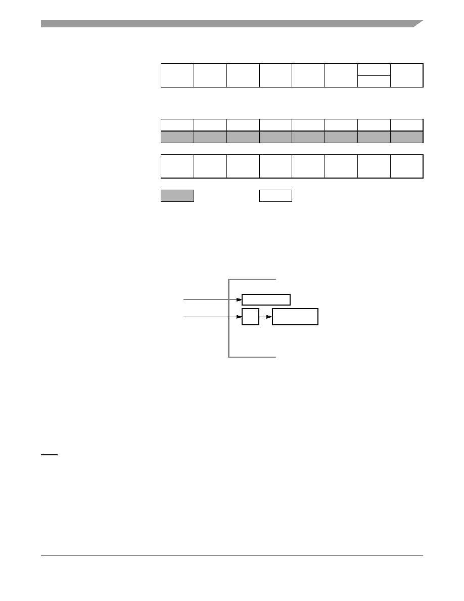
SIM Bus Clock Control and Generation
MC68HC908LB8 Data Sheet, Rev. 0
Freescale Semiconductor
171
17.2 SIM Bus Clock Control and Generation
The bus clock generator provides system clock signals for the CPU and peripherals on the MCU. The
system clocks are generated from an incoming clock, BUSCLKX2, as shown in
Figure 17-3
.
Figure 17-3. SIM Clock Signals
17.2.1 Bus Timing
In user mode, the internal bus frequency is the oscillator frequency (BUSCLKX4) divided by four.
17.2.2 Clock Start-Up from POR
When the power-on reset module generates a reset, the clocks to the CPU and peripherals are inactive
and held in an inactive phase until after the 4096 BUSCLKX4 cycle POR time out has completed. The
RST pin is driven low by the SIM during this entire period. The IBUS clocks start upon completion of the
time out.
17.2.3 Clocks in Stop Mode and Wait Mode
Upon exit from stop mode by an interrupt or reset, the SIM allows BUSCLKX4 to clock the SIM counter.
The CPU and peripheral clocks do not become active until after the stop delay time out. This time out is
selectable as 4096 or 32 BUSCLKX4 cycles. See
17.6.2 Stop Mode
.
Addr.
Register Name
Bit 7
6
5
4
3
2
1
Bit 0
$FE00
Break Status Register
(BSR)
See page 181.
Read:
R
R
R
R
R
R
SBSW
R
Write:
Note
(1)
Reset:
0
0
0
0
0
0
0
0
1. Writing a 0 clears SBSW.
$FE01
SIM Reset Status
Register (SRSR)
See page 182.
Read:
POR
PIN
COP
ILOP
ILAD
MODRST
LVI
0
Write:
POR:
1
0
0
0
0
0
0
0
$FE03
Break Flag Control Register
(BFCR)
See page 183.
Read:
BCFE
R
R
R
R
R
R
R
Write:
Reset:
0
= Unimplemented
R
= Reserved
Figure 17-2. SIM I/O Register Summary
˜
2
BUS CLOCK
GENERATORS
SIM
SIM COUNTER
FROM
OSCILLATOR
FROM
OSCILLATOR
BUSCLKX2
BUSCLKX4

System Integration Module (SIM)
MC68HC908LB8 Data Sheet, Rev. 0
172
Freescale Semiconductor
In wait mode, the CPU clocks are inactive. The SIM also produces two sets of clocks for other modules.
Refer to the wait mode subsection of each module to see if the module is active or inactive in wait mode.
Some modules can be programmed to be active in wait mode.
17.3 Reset and System Initialization
The MCU has these reset sources:
∑
Power-on reset module (POR)
∑
External reset pin (RST)
∑
Computer operating properly module (COP)
∑
Low-voltage inhibit module (LVI)
∑
Illegal opcode
∑
Illegal address
∑
Forced monitor mode entry reset (MODRST)
All of these resets produce the vector $FFFE:$FFFF ($FEFE:$FEFF in monitor mode) and assert the
internal reset signal (IRST). IRST causes all registers to be returned to their default values and all
modules to be returned to their reset states.
An internal reset clears the SIM counter (see
17.4 SIM Counter
), but an external reset does not. Each of
the resets sets a corresponding bit in the SIM reset status register (SRSR). See
17.7 SIM Registers.
17.3.1 External Pin Reset
The RST pin circuit includes an internal pullup device. Pulling the asynchronous RST pin low halts all
processing. The PIN bit of the SIM reset status register (SRSR) is set as long as RST is held low for a
minimum of 67 BUSCLKX4 cycles, assuming that neither the POR nor the LVI was the source of the reset.
See
Table 17-2
for details.
Figure 17-4
shows the relative timing.
Figure 17-4. External Reset Timing
17.3.2 Active Resets from Internal Sources
All internal reset sources actively pull the RST pin low for 32 BUSCLKX4 cycles to allow resetting of
external peripherals. The internal reset signal IRST continues to be asserted for an additional 32 cycles.
Table 17-2. PIN Bit Set Timing
Reset Type
Number of Cycles Required to Set PIN
POR/LVI
4163 (4096 + 64 + 3)
All others
67 (64 + 3)
RST
IAB
PC
VECT H VECT L
BUSCLKX2

Reset and System Initialization
MC68HC908LB8 Data Sheet, Rev. 0
Freescale Semiconductor
173
See
Figure 17-5
. An internal reset can be caused by an illegal address, illegal opcode, COP timeout, LVI,
or POR. See
Figure 17-6
.
NOTE
For LVI or POR resets, the SIM cycles through 4096 + 32 BUSCLKX4
cycles during which the SIM forces the RST pin low. The internal reset
signal then follows the sequence from the falling edge of RST shown in
Figure 17-5
.
Figure 17-5. Internal Reset Timing
The COP reset is asynchronous to the bus clock.
Figure 17-6. Sources of Internal Reset
The active reset feature allows the part to issue a reset to peripherals and other chips within a system
built around the MCU.
17.3.2.1 Power-On Reset
When power is first applied to the MCU, the power-on reset module (POR) generates a pulse to indicate
that power-on has occurred. The external reset pin (RST) is held low while the SIM counter counts out
4096 + 32 BUSCLKX4 cycles. Thirty-two BUSCLKX4 cycles later, the CPU and memories are released
from reset to allow the reset vector sequence to occur.
At power-on, these events occur:
∑
A POR pulse is generated.
∑
The internal reset signal is asserted.
∑
The SIM enables the oscillator to drive BUSCLKX4.
∑
Internal clocks to the CPU and modules are held inactive for 4096 BUSCLKX4 cycles to allow
stabilization of the oscillator.
∑
The RST pin is driven low during the oscillator stabilization time.
∑
The POR bit of the SIM reset status register (SRSR) is set and all other bits in the register are
cleared.
IRST
RST
RST PULLED LOW BY MCU
IAB
32 CYCLES
32 CYCLES
VECTOR HIGH
BUSCLKX4
ILLEGAL ADDRESS RST
ILLEGAL OPCODE RST
COPRST
LVI
POR
INTERNAL RESET
MODRST

System Integration Module (SIM)
MC68HC908LB8 Data Sheet, Rev. 0
174
Freescale Semiconductor
Figure 17-7. POR Recovery
17.3.2.2 Computer Operating Properly (COP) Reset
An input to the SIM is reserved for the COP reset signal. The overflow of the COP counter causes an
internal reset and sets the COP bit in the SIM reset status register (SRSR). The SIM actively pulls down
the RST pin for all internal reset sources.
The COP module is disabled if the IRQ pin is held at V
TST
while the MCU is in monitor mode. The COP
module can be disabled only through combinational logic conditioned with the high voltage signal on the
IRQ pin. This prevents the COP from becoming disabled as a result of external noise.
17.3.2.3 Illegal Opcode Reset
The SIM decodes signals from the CPU to detect illegal instructions. An illegal instruction sets the ILOP
bit in the SIM reset status register (SRSR) and causes a reset.
If the stop enable bit, STOP, in the mask option register is 0, the SIM treats the STOP instruction as an
illegal opcode and causes an illegal opcode reset. The SIM actively pulls down the RST pin for all internal
reset sources.
17.3.2.4 Illegal Address Reset
An opcode fetch from an unmapped address generates an illegal address reset. The SIM verifies that the
CPU is fetching an opcode prior to asserting the ILAD bit in the SIM reset status register (SRSR) and
resetting the MCU. A data fetch from an unmapped address does not generate a reset. The SIM actively
pulls down the RST pin for all internal reset sources.
17.3.2.5 Low-Voltage Inhibit (LVI) Reset
The low-voltage inhibit module (LVI) asserts its output to the SIM when the V
DD
voltage falls to the
LVI
TRIPF
voltage. The LVI bit in the SIM reset status register (SRSR) is set, and the external reset pin
(RST) is held low while the SIM counter counts out 4096 + 32 BUSCLKX4 cycles. Thirty-two BUSCLKX4
PORRST
OSC1
BUSCLKX4
BUSCLKX2
RST
IAB
4096
CYCLES
32
CYCLES
$FFFE
$FFFF

SIM Counter
MC68HC908LB8 Data Sheet, Rev. 0
Freescale Semiconductor
175
cycles later, the CPU is released from reset to allow the reset vector sequence to occur. The SIM actively
pulls down the RST pin for all internal reset sources.
17.3.2.6 Monitor Mode Entry Module Reset (MODRST)
The monitor mode entry module reset (MODRST) asserts its output to the SIM when monitor mode is
entered in the condition where the reset vectors are erased ($FF). When MODRST gets asserted, an
internal reset occurs. The SIM actively pulls down the RST pin for all internal reset sources.
17.4 SIM Counter
The SIM counter is used by the power-on reset module (POR) and in stop mode recovery to allow the
oscillator time to stabilize before enabling the internal bus (IBUS) clocks. The SIM counter is 13 bits long.
17.4.1 SIM Counter During Power-On Reset
The power-on reset module (POR) detects power applied to the MCU. At power-on, the POR circuit
asserts the signal PORRST. Once the SIM is initialized, it enables the clock generation module (CGM) to
drive the bus clock state machine.
17.4.2 SIM Counter During Stop Mode Recovery
The SIM counter also is used for stop mode recovery. The STOP instruction clears the SIM counter. After
an interrupt, break, or reset, the SIM senses the state of the short stop recovery bit, SSREC, in the mask
option register. If the SSREC bit is a 1, then the stop recovery is reduced from the normal delay of 4096
BUSCLKX4 cycles down to 32 BUSCLKX4 cycles. This is ideal for applications using canned oscillators
that do not require long startup times from stop mode. External crystal applications should use the full
stop recovery time, that is, with SSREC cleared.
17.4.3 SIM Counter and Reset States
External reset has no effect on the SIM counter. See
17.6.2 Stop Mode
for details. The SIM counter is
free-running after all reset states. See
17.3.2 Active Resets from Internal Sources
for counter control and
internal reset recovery sequences.
17.5 Exception Control
Normal, sequential program execution can be changed in three different ways:
∑
Interrupts:
≠
Maskable hardware CPU interrupts
≠
Non-maskable software interrupt instruction (SWI)
∑
Reset
∑
Break interrupts
17.5.1 Interrupts
At the beginning of an interrupt, the CPU saves the CPU register contents on the stack and sets the
interrupt mask (I bit) to prevent additional interrupts. At the end of an interrupt, the RTI instruction recovers
the CPU register contents from the stack so that normal processing can resume.
Figure 17-8
shows
interrupt entry timing.
Figure 17-9
shows interrupt recovery timing.

System Integration Module (SIM)
MC68HC908LB8 Data Sheet, Rev. 0
176
Freescale Semiconductor
Figure 17-8
.
Interrupt Entry Timing
Figure 17-9. Interrupt Recovery Timing
Interrupts are latched, and arbitration is performed in the SIM at the start of interrupt processing. The
arbitration result is a constant that the CPU uses to determine which vector to fetch. Once an interrupt is
latched by the SIM, no other interrupt can take precedence, regardless of priority, until the latched
interrupt is serviced (or the I bit is cleared). See
Figure 17-10
.
17.5.1.1 Hardware Interrupts
A hardware interrupt does not stop the current instruction. Processing of a hardware interrupt begins after
completion of the current instruction. When the current instruction is complete, the SIM checks all pending
hardware interrupts. If interrupts are not masked (I bit clear in the condition code register) and if the
corresponding interrupt enable bit is set, the SIM proceeds with interrupt processing; otherwise, the next
instruction is fetched and executed.
If more than one interrupt is pending at the end of an instruction execution, the highest priority interrupt is
serviced first.
Figure 17-11
demonstrates what happens when two interrupts are pending. If an interrupt
is pending upon exit from the original interrupt service routine, the pending interrupt is serviced before the
LDA instruction is executed.
MODULE
IDB
R/W
INTERRUPT
DUMMY
SP
SP ≠ 1
SP ≠ 2
SP ≠ 3
SP ≠ 4
VECT H
VECT L
START ADDR
IAB
DUMMY
PC ≠ 1[7:0] PC ≠ 1[15:8]
X
A
CCR
V DATA H
V DATA L
OPCODE
I BIT
MODULE
IDB
R/W
INTERRUPT
SP ≠ 4
SP ≠ 3
SP ≠ 2
SP ≠ 1
SP
PC
PC + 1
IAB
CCR
A
X
PC ≠ 1 [7:0] PC ≠ 1 [15:8] OPCODE
OPERAND
I BIT

Exception Control
MC68HC908LB8 Data Sheet, Rev. 0
Freescale Semiconductor
177
Figure 17-10. Interrupt Processing
NO
NO
YES
NO
NO
YES
NO
YES
AS MANY INTERRUPTS
I BIT SET?
FROM RESET
BREAK
I BIT SET?
IRQ
INTERRUPT?
SWI
INSTRUCTION?
RTI
INSTRUCTION?
FETCH NEXT
INSTRUCTION
UNSTACK CPU REGISTERS
STACK CPU REGISTERS
SET I BIT
LOAD PC WITH INTERRUPT VECTOR
EXECUTE INSTRUCTION
YES
YES
AS EXIST ON CHIP
INTERRUPT?
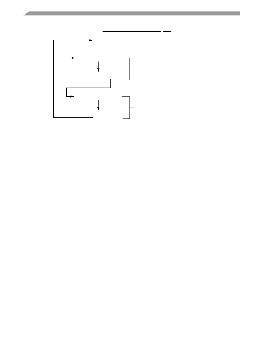
System Integration Module (SIM)
MC68HC908LB8 Data Sheet, Rev. 0
178
Freescale Semiconductor
Figure 17-11
.
Interrupt Recognition Example
The LDA opcode is prefetched by both the INT1 and INT2 RTI instructions. However, in the case of the
INT1 RTI prefetch, this is a redundant operation.
NOTE
To maintain compatibility with the M6805 Family, the H register is not
pushed on the stack during interrupt entry. If the interrupt service routine
modifies the H register or uses the indexed addressing mode, software
should save the H register and then restore it prior to exiting the routine.
17.5.1.2 SWI Instruction
The SWI instruction is a non-maskable instruction that causes an interrupt regardless of the state of the
interrupt mask (I bit) in the condition code register.
NOTE
A software interrupt pushes PC onto the stack. A software interrupt does
not push PC ≠ 1, as a hardware interrupt does.
17.5.2 Reset
All reset sources always have equal and highest priority and cannot be arbitrated.
17.5.3 Break Interrupts
The break module can stop normal program flow at a software-programmable break point by asserting its
break interrupt output (see
19.2 Break Module (BRK)
). The SIM puts the CPU into the break state by
forcing it to the SWI vector location. Refer to the break interrupt subsection of each module to see how
each module is affected by the break state.
CLI
LDA
INT1
PULH
RTI
INT2
BACKGROUND
#$FF
PSHH
INT1 INTERRUPT SERVICE ROUTINE
PULH
RTI
PSHH
INT2 INTERRUPT SERVICE ROUTINE
ROUTINE

Low-Power Modes
MC68HC908LB8 Data Sheet, Rev. 0
Freescale Semiconductor
179
17.5.4 Status Flag Protection in Break Mode
The SIM controls whether status flags contained in other modules can be cleared during break mode. The
user can select whether flags are protected from being cleared by properly initializing the break clear flag
enable bit (BCFE) in the SIM break flag control register (SBFCR).
Protecting flags in break mode ensures that set flags will not be cleared while in break mode. This
protection allows registers to be freely read and written during break mode without losing status flag
information.
Setting the BCFE bit enables the clearing mechanisms. Once cleared in break mode, a flag remains
cleared even when break mode is exited. Status flags with a 2-step clearing mechanism -- for example,
a read of one register followed by the read or write of another -- are protected, even when the first step
is accomplished prior to entering break mode. Upon leaving break mode, execution of the second step
will clear the flag as normal.
17.6 Low-Power Modes
Executing the WAIT or STOP instruction puts the MCU in a low power-consumption mode for standby
situations. The SIM holds the CPU in a non-clocked state. The operation of each of these modes is
described in the following subsections. Both STOP and WAIT clear the interrupt mask (I) in the condition
code register, allowing interrupts to occur.
17.6.1 Wait Mode
In wait mode, the CPU clocks are inactive while the peripheral clocks continue to run.
Figure 17-12
shows
the timing for wait mode entry.
A module that is active during wait mode can wakeup the CPU with an interrupt if the interrupt is enabled.
Stacking for the interrupt begins one cycle after the WAIT instruction during which the interrupt occurred.
In wait mode, the CPU clocks are inactive. Refer to the wait mode subsection of each module to see if the
module is active or inactive in wait mode. Some modules can be programmed to be active in wait mode.
Wait mode also can be exited by a reset (or break in emulation mode). A break interrupt during wait mode
sets the SIM break stop/wait bit, SBSW, in the SIM break status register (SBSR). If the COP disable bit,
COPD, in the mask option register is 0, then the computer operating properly module (COP) is enabled
and remains active in wait mode.
Figure 17-13
and
Figure 17-14
show the timing for WAIT recovery.
Figure 17-12. Wait Mode Entry Timing
WAIT ADDR + 1
SAME
SAME
IAB
IDB
PREVIOUS DATA
NEXT OPCODE
SAME
WAIT ADDR
SAME
R/W
Note: Previous data can be operand data or the WAIT opcode, depending on the
last instruction.

System Integration Module (SIM)
MC68HC908LB8 Data Sheet, Rev. 0
180
Freescale Semiconductor
Figure 17-13. Wait Recovery from Interrupt
Figure 17-14. Wait Recovery from Internal Reset
17.6.2 Stop Mode
In stop mode, the SIM counter is reset and the system clocks are disabled. An interrupt request from a
module can cause an exit from stop mode. Stacking for interrupts begins after the selected stop recovery
time has elapsed. Reset also causes an exit from stop mode.
The SIM disables the clock generator module outputs (BUSCLKX2 and BUSCLKX4) in stop mode,
stopping the CPU and peripherals. Stop recovery time is selectable using the SSREC bit in the mask
option register (MOR). If SSREC is set, stop recovery is reduced from the normal delay of 4096
BUSCLKX4 cycles down to 32. This is ideal for applications using canned oscillators that do not require
long startup times from stop mode.
NOTE
External crystal applications should use the full stop recovery time by
clearing the SSREC bit.
The SIM counter is held in reset from the execution of the STOP instruction until the beginning of stop
recovery. It is then used to time the recovery period.
Figure 17-15
shows stop mode entry timing.
Figure 17-16
shows stop mode recovery time from interrupt or break.
NOTE
To minimize stop current, all pins configured as inputs should be driven to
a logic 1 or logic 0.
$6E0C
$6E0B
$00FF
$00FE
$00FD
$00FC
$A6
$A6
$01
$0B
$6E
$A6
IAB
IDB
EXITSTOPWAIT
Note: EXITSTOPWAIT = RST pin or CPU interrupt
IAB
IDB
RST
$A6
$A6
$6E0B
RST VCT H
RST VCT L
$A6
BUSCLKX4
32
CYCLES
32
CYCLES

SIM Registers
MC68HC908LB8 Data Sheet, Rev. 0
Freescale Semiconductor
181
Figure 17-15. Stop Mode Entry Timing
Figure 17-16. Stop Mode Recovery from Interrupt
17.7 SIM Registers
The SIM has three memory-mapped registers.
Table 17-3
shows the mapping of these registers.
17.7.1 Break Status Register
The break status register (BSR) contains a flag to indicate that a break caused an exit from wait mode.
This register is only used in emulation mode.
Table 17-3. SIM Registers
Address
Register
Access Mode
$FE00
BSR
User
$FE01
SRSR
User
$FE03
BFCR
User
Address:
$FE00
Bit 7
6
5
4
3
2
1
Bit 0
Read:
R
R
R
R
R
R
SBSW
R
Write:
Note
(1)
Reset:
0
0
0
0
0
0
0
0
R
= Reserved
1. Writing a 0 clears SBSW.
Figure 17-17. Break Status Register (BSR)
STOP ADDR + 1
SAME
SAME
IAB
IDB
PREVIOUS DATA
NEXT OPCODE
SAME
STOP ADDR
SAME
R/W
CPUSTOP
Note: Previous data can be operand data or the STOP opcode, depending
on the last instruction.
BUSCLKX4
INT/BREAK
IAB
STOP + 2
STOP + 2
SP
SP ≠ 1
SP ≠ 2
SP ≠ 3
STOP +1
STOP RECOVERY PERIOD

System Integration Module (SIM)
MC68HC908LB8 Data Sheet, Rev. 0
182
Freescale Semiconductor
SBSW -- SIM Break Stop/Wait
This status bit is useful in applications requiring a return to wait mode after exiting from a break
interrupt. Clear SBSW by writing a 0 to it. Reset clears SBSW.
1 = Wait mode was exited by break interrupt.
0 = Wait mode was not exited by break interrupt.
SBSW can be read within the break state SWI routine. The user can modify the return address on the
stack by subtracting one from it.
17.7.2 SIM Reset Status Register
This register contains six flags that show the source of the last reset provided all previous reset status bits
have been cleared. Clear the SIM reset status register by reading it. A power-on reset sets the POR bit
and clears all other bits in the register.
POR -- Power-On Reset Bit
1 = Last reset caused by POR circuit
0 = Read of SRSR
PIN -- External Reset Bit
1 = Last reset caused by external reset pin (RST)
0 = POR or read of SRSR
COP -- Computer Operating Properly Reset Bit
1 = Last reset caused by COP counter
0 = POR or read of SRSR
ILOP -- Illegal Opcode Reset Bit
1 = Last reset caused by an illegal opcode
0 = POR or read of SRSR
ILAD -- Illegal Address Reset Bit (opcode fetches only)
1 = Last reset caused by an opcode fetch from an illegal address
0 = POR or read of SRSR
MODRST -- Monitor Mode Entry Module Reset Bit
1 = Last reset caused by monitor mode entry when vector locations $FFFE and $FFFF are $FF after
POR while IRQ = V
DD
0 = POR or read of SRSR
LVI -- Low-Voltage Inhibit Reset Bit
1 = Last reset caused by the LVI circuit
0 = POR or read of SRSR
Address:
$FE01
Bit 7
6
5
4
3
2
1
Bit 0
Read:
POR
PIN
COP
ILOP
ILAD
MODRST
LVI
0
Write:
Reset:
1
0
0
0
0
0
0
0
= Unimplemented
Figure 17-18. SIM Reset Status Register (SRSR)

SIM Registers
MC68HC908LB8 Data Sheet, Rev. 0
Freescale Semiconductor
183
17.7.3 Break Flag Control Register
The break control register contains a bit that enables software to clear status bits while the MCU is in a
break state.
BCFE -- Break Clear Flag Enable Bit
This read/write bit enables software to clear status bits by accessing status registers while the MCU is
in a break state. To clear status bits during the break state, the BCFE bit must be set.
1 = Status bits clearable during break
0 = Status bits not clearable during break
Address:
$FE03
Bit 7
6
5
4
3
2
1
Bit 0
Read:
BCFE
R
R
R
R
R
R
R
Write:
Reset:
0
R
= Reserved
Figure 17-19. Break Flag Control Register (BFCR)

System Integration Module (SIM)
MC68HC908LB8 Data Sheet, Rev. 0
184
Freescale Semiconductor

MC68HC908LB8 Data Sheet, Rev. 0
Freescale Semiconductor
185
Chapter 18
Timer Interface Module (TIM)
18.1 Introduction
This section describes the timer interface (TIM) module. The TIM is a two-channel timer (only one of the
channels is connected to an input/output pin) that provides a timing reference with input capture, output
compare, and pulse-width-modulation (PWM) functions.
Figure 18-2
is a block diagram of the TIM.
Figure 18-1. Block Diagram Highlighting TIM Block and Pins
M68HC08 CPU
CONTROL AND STATUS
USER FLASH -- 8 KBYTES
USER RAM -- 128 BYTES
MONITOR ROM -- 350 BYTES
USER FLASH VECTOR SPACE -- 34 BYTES
DDRB
PO
R
T
B
DDRC
PORT
C
INTERNAL BUS
PTA6
(1)
/AD5/TCH0/KBI6
PTA5
(1)
/RST/KBI5
PTA4
(1)
/AD4/KBI4
PTA3
(1)
/AD3/KBI3
PTA2
(1)
/AD2/KBI2
PTA1
(1)
/AD1/KBI1
PTA0
(1)
/AD0/KBI0
PTB7/V
OUT
/AD6/FAULT
(2)
PTB6/V≠
PTB5/V+
PTB4/PWM1
PTB3/PWM0
PTB2/FAULT
(2)
PTB1/BOT
PTB0/TOP
PTC1
(1)
/OSC2
PTC0
(1)
/OSC1
POWER
V
SS
V
DD
DDRA
PO
R
T
A
PTC2
(1)
/SHTDWN/IRQ
FLASH PROGRAMMING
OSCILLATOR
CPU
REGISTERS
ARITHMETIC/LOGIC
UNIT (ALU)
SYSTEM INTEGRATION
MODULE
DUAL CHANNEL PWM
MODULE
HIGH RESOLUTION PWM
MODULE
LOW-VOLTAGE INHIBIT
MODULE
COMPUTER OPERATING
PROPERLY MODULE
2-CHANNEL TIMER
MODULE
8-BIT ANALOG-TO-DIGITAL
CONVERTER MODULE
OP AMP/COMPARATOR
MODULE
KEYBOARD INTERRUPT
MODULE
MODULE
ROUTINES ROM -- 674 BYTES
REGISTERS -- 64 BYTES
1. Pin contains integrated pullup device.
2. Fault function switchable between pins PTB2 and PTB7.
Notes:

Timer Interface Module (TIM)
MC68HC908LB8 Data Sheet, Rev. 0
186
Freescale Semiconductor
18.2 Features
Features of the TIM include:
∑
One input capture/output compare channels:
≠
Rising-edge, falling-edge, or any-edge input capture trigger
≠
Set, clear, or toggle output compare action
∑
Buffered and unbuffered pulse-width-modulation (PWM) signal generation
∑
Programmable TIM clock input with 7-frequency internal bus clock prescaler selection
∑
Free-running or modulo up-count operation
∑
Toggle any channel pin on overflow
∑
TIM counter stop and reset bits
Figure 18-2. TIM Block Diagram
18.3 Functional Description
Figure 18-2
shows the structure of the TIM. The central component of the TIM is the 16-bit TIM counter
that can operate as a free-running counter or a modulo up-counter. The TIM counter provides the timing
reference for the input capture and output compare functions. The TIM counter modulo registers,
PRESCALER
PRESCALER SELECT
INTERNAL
16-BIT COMPARATOR
PS2
PS1
PS0
16-BIT COMPARATOR
16-BIT LATCH
TCH0H:TCH0L
MS0A
ELS0B
ELS0A
TOF
TOIE
16-BIT COMPARATOR
16-BIT LATCH
TCH1H:TCH1L
CHANNEL 0
CHANNEL 1
TMODH:TMODL
TRST
TSTOP
TOV0
CH0IE
CH0F
ELS1B
ELS1A
TOV1
CH1IE
CH1MAX
CH1F
CH0MAX
MS0B
16-BIT COUNTER
IN
TERNAL BUS
BUS CLOCK
MS1A
TCH0
TCH1
INTERRUPT
LOGIC
PORT
LOGIC
INTERRUPT
LOGIC
INTERRUPT
LOGIC
PORT
LOGIC
(Not available
on port pin)

Functional Description
MC68HC908LB8 Data Sheet, Rev. 0
Freescale Semiconductor
187
TMODH:TMODL, control the modulo value of the TIM counter. Software can read the TIM counter value
at any time without affecting the counting sequence.
The two TIM channels are programmable independently as input capture or output compare channels. If
a channel is configured as input capture, then an internal pullup device may be enabled for that channel. .
Figure 18-3
summarizes the timer registers.
Addr.
Register Name
Bit 7
6
5
4
3
2
1
Bit 0
$0020
Timer Status and Control
Register (T1SC)
See page 193.
Read:
TOF
TOIE
TSTOP
0
0
PS2
PS1
PS0
Write:
0
TRST
Reset:
0
0
1
0
0
0
0
0
$0021
Timer Counter
Register High (T1CNTH)
See page 194.
Read:
Bit 15
14
13
12
11
10
9
Bit 8
Write:
Reset:
0
0
0
0
0
0
0
0
$0022
Timer Counter
Register Low (T1CNTL)
See page 194.
Read:
Bit 7
6
5
4
3
2
1
Bit 0
Write:
Reset:
0
0
0
0
0
0
0
0
$0023
Timer Counter Modulo
Register High (T1MODH)
See page 195.
Read:
Bit 15
14
13
12
11
10
9
Bit 8
Write:
Reset:
1
1
1
1
1
1
1
1
$0024
Timer Counter Modulo
Register Low (T1MODL)
See page 195.
Read:
Bit 7
6
5
4
3
2
1
Bit 0
Write:
Reset:
1
1
1
1
1
1
1
1
$0025
Timer Channel 0 Status and
Control Register (T1SC0)
See page 196.
Read:
CH0F
CH0IE
MS0B
MS0A
ELS0B
ELS0A
TOV0
CH0MAX
Write:
0
Reset:
0
0
0
0
0
0
0
0
$0026
Timer Channel 0
Register High (T1CH0H)
See page 199.
Read:
Bit 15
14
13
12
11
10
9
Bit 8
Write:
Reset:
Indeterminate after reset
$0027
Timer Channel 0
Register Low (T1CH0L)
See page 199.
Read:
Bit 7
6
5
4
3
2
1
Bit 0
Write:
Reset:
Indeterminate after reset
$0028
Timer Channel 1 Status and
Control Register (T1SC1)
See page 196.
Read:
CH1F
CH1IE
0
MS1A
ELS1B
ELS1A
TOV1
CH1MAX
Write:
0
Reset:
0
0
0
0
0
0
0
0
= Unimplemented
Figure 18-3. TIM I/O Register Summary (Sheet 1 of 2)

Timer Interface Module (TIM)
MC68HC908LB8 Data Sheet, Rev. 0
188
Freescale Semiconductor
18.3.1 TIM Counter Prescaler
The TIM clock source can be one of the seven prescaler outputs. The prescaler generates seven clock
rates from the internal bus clock. The prescaler select bits, PS[2:0], in the TIM status and control register
select the TIM clock source.
18.3.2 Input Capture
With the input capture function, the TIM can capture the time at which an external event occurs. When an
active edge occurs on the pin of an input capture channel, the TIM latches the contents of the TIM counter
into the TIM channel registers, TCHxH:TCHxL. The polarity of the active edge is programmable. Input
captures can generate TIM CPU interrupt requests.
18.3.3 Output Compare
With the output compare function, the TIM can generate a periodic pulse with a programmable polarity,
duration, and frequency. When the counter reaches the value in the registers of an output compare
channel, the TIM can set, clear, or toggle the channel pin. Output compares can generate TIM CPU
interrupt requests.
18.3.3.1 Unbuffered Output Compare
Any output compare channel can generate unbuffered output compare pulses as described in
18.3.3
Output Compare
. The pulses are unbuffered because changing the output compare value requires writing
the new value over the old value currently in the TIM channel registers.
An unsynchronized write to the TIM channel registers to change an output compare value could cause
incorrect operation for up to two counter overflow periods. For example, writing a new value before the
counter reaches the old value but after the counter reaches the new value prevents any compare during
that counter overflow period. Also, using a TIM overflow interrupt routine to write a new, smaller output
compare value may cause the compare to be missed. The TIM may pass the new value before it is written.
Use the following methods to synchronize unbuffered changes in the output compare value on channel x:
∑
When changing to a smaller value, enable channel x output compare interrupts and write the new
value in the output compare interrupt routine. The output compare interrupt occurs at the end of
the current output compare pulse. The interrupt routine has until the end of the counter overflow
period to write the new value.
$0029
Timer Channel 1
Register High (T1CH1H)
See page 199.
Read:
Bit 15
14
13
12
11
10
9
Bit 8
Write:
Reset:
Indeterminate after reset
$002A
Timer Channel 1
Register Low (T1CH1L)
See page 199.
Read:
Bit 7
6
5
4
3
2
1
Bit 0
Write:
Reset:
Indeterminate after reset
Addr.
Register Name
Bit 7
6
5
4
3
2
1
Bit 0
= Unimplemented
Figure 18-3. TIM I/O Register Summary (Sheet 2 of 2)

Functional Description
MC68HC908LB8 Data Sheet, Rev. 0
Freescale Semiconductor
189
∑
When changing to a larger output compare value, enable TIM overflow interrupts and write the new
value in the TIM overflow interrupt routine. The TIM overflow interrupt occurs at the end of the
current counter overflow period. Writing a larger value in an output compare interrupt routine (at
the end of the current pulse) could cause two output compares to occur in the same counter
overflow period.
18.3.3.2 Buffered Output Compare
Channels 0 and 1 can be linked to form a buffered output compare channel whose output appears on the
TCH0 pin. The TIM channel registers of the linked pair alternately control the output.
Setting the MS0B bit in TIM channel 0 status and control register (TSC0) links channel 0 and channel 1.
The output compare value in the TIM channel 0 registers initially controls the output on the TCH0 pin.
Writing to the TIM channel 1 registers enables the TIM channel 1 registers to synchronously control the
output after the TIM overflows. At each subsequent overflow, the TIM channel registers (0 or 1) that
control the output are the ones written to last. TSC0 controls and monitors the buffered output compare
function, and TIM channel 1 status and control register (TSC1) is unused.
NOTE
In buffered output compare operation, do not write new output compare
values to the currently active channel registers. User software should track
the currently active channel to prevent writing a new value to the active
channel. Writing to the active channel registers is the same as generating
unbuffered output compares.
18.3.4 Pulse Width Modulation (PWM)
By using the toggle-on-overflow feature with an output compare channel, the TIM can generate a PWM
signal. The value in the TIM counter modulo registers determines the period of the PWM signal. The
channel pin toggles when the counter reaches the value in the TIM counter modulo registers. The time
between overflows is the period of the PWM signal.
As
Figure 18-4
shows, the output compare value in the TIM channel registers determines the pulse width
of the PWM signal. The time between overflow and output compare is the pulse width. Program the TIM
to clear the channel pin on output compare if the state of the PWM pulse is logic 1. Program the TIM to
set the pin if the state of the PWM pulse is logic 0.
Figure 18-4. PWM Period and Pulse Width
TCHx
PERIOD
PULSE
WIDTH
OVERFLOW
OVERFLOW
OVERFLOW
OUTPUT
COMPARE
OUTPUT
COMPARE
OUTPUT
COMPARE

Timer Interface Module (TIM)
MC68HC908LB8 Data Sheet, Rev. 0
190
Freescale Semiconductor
The value in the TIM counter modulo registers and the selected prescaler output determines the
frequency of the PWM output. The frequency of an 8-bit PWM signal is variable in 256 increments. Writing
$00FF (255) to the TIM counter modulo registers produces a PWM period of 256 times the internal bus
clock period if the prescaler select value is $000. See
18.8.1 TIM Status and Control Register
.
The value in the TIM channel registers determines the pulse width of the PWM output. The pulse width of
an 8-bit PWM signal is variable in 256 increments. Writing $0080 (128) to the TIM channel registers
produces a duty cycle of 128/256 or 50%.
18.3.4.1 Unbuffered PWM Signal Generation
Any output compare channel can generate unbuffered PWM pulses as described in
18.3.4 Pulse Width
Modulation (PWM)
. The pulses are unbuffered because changing the pulse width requires writing the new
pulse width value over the old value currently in the TIM channel registers.
An unsynchronized write to the TIM channel registers to change a pulse width value could cause incorrect
operation for up to two PWM periods. For example, writing a new value before the counter reaches the
old value but after the counter reaches the new value prevents any compare during that PWM period.
Also, using a TIM overflow interrupt routine to write a new, smaller pulse width value may cause the
compare to be missed. The TIM may pass the new value before it is written.
Use the following methods to synchronize unbuffered changes in the PWM pulse width on channel x:
∑
When changing to a shorter pulse width, enable channel x output compare interrupts and write the
new value in the output compare interrupt routine. The output compare interrupt occurs at the end
of the current pulse. The interrupt routine has until the end of the PWM period to write the new
value.
∑
When changing to a longer pulse width, enable TIM overflow interrupts and write the new value in
the TIM overflow interrupt routine. The TIM overflow interrupt occurs at the end of the current PWM
period. Writing a larger value in an output compare interrupt routine (at the end of the current pulse)
could cause two output compares to occur in the same PWM period.
NOTE
In PWM signal generation, do not program the PWM channel to toggle on
output compare. Toggling on output compare prevents reliable 0% duty
cycle generation and removes the ability of the channel to self-correct in the
event of software error or noise. Toggling on output compare also can
cause incorrect PWM signal generation when changing the PWM pulse
width to a new, much larger value.
18.3.4.2 Buffered PWM Signal Generation
Channels 0 and 1 can be linked to form a buffered PWM channel whose output appears on the TCH0 pin.
The TIM channel registers of the linked pair alternately control the pulse width of the output.
Setting the MS0B bit in TIM channel 0 status and control register (TSC0) links channel 0 and channel 1.
The TIM channel 0 registers initially control the pulse width on the TCH0 pin. Writing to the TIM channel
1 registers enables the TIM channel 1 registers to synchronously control the pulse width at the beginning
of the next PWM period. At each subsequent overflow, the TIM channel registers (0 or 1) that control the
pulse width are the ones written to last. TSC0 controls and monitors the buffered PWM function, and TIM
channel 1 status and control register (TSC1) is unused.

Interrupts
MC68HC908LB8 Data Sheet, Rev. 0
Freescale Semiconductor
191
NOTE
In buffered PWM signal generation, do not write new pulse width values to
the currently active channel registers. User software should track the
currently active channel to prevent writing a new value to the active
channel. Writing to the active channel registers is the same as generating
unbuffered PWM signals.
18.3.4.3 PWM Initialization
To ensure correct operation when generating unbuffered or buffered PWM signals, use the following
initialization procedure:
1.
In the TIM status and control register (TSC):
a.
Stop the TIM counter by setting the TIM stop bit, TSTOP.
b.
Reset the TIM counter and prescaler by setting the TIM reset bit, TRST.
2.
In the TIM counter modulo registers (TMODH:TMODL), write the value for the required PWM
period.
3.
In the TIM channel x registers (TCHxH:TCHxL), write the value for the required pulse width.
4.
In TIM channel x status and control register (TSCx):
a.
Write 0:1 (for unbuffered output compare or PWM signals) or 1:0 (for buffered output compare
or PWM signals) to the mode select bits, MSxB:MSxA. See
Table 18-2
.
b.
Write 1 to the toggle-on-overflow bit, TOVx.
c.
Write 1:0 (to clear output on compare) or 1:1 (to set output on compare) to the edge/level
select bits, ELSxB:ELSxA. The output action on compare must force the output to the
complement of the pulse width level. See
Table 18-2
.
NOTE
In PWM signal generation, do not program the PWM channel to toggle on
output compare. Toggling on output compare prevents reliable 0% duty
cycle generation and removes the ability of the channel to self-correct in the
event of software error or noise. Toggling on output compare can also
cause incorrect PWM signal generation when changing the PWM pulse
width to a new, much larger value.
5.
In the TIM status control register (TSC), clear the TIM stop bit, TSTOP.
Setting MS0B links channels 0 and 1 and configures them for buffered PWM operation. The TIM channel
0 registers (TCH0H:TCH0L) initially control the buffered PWM output. TIM status control register 0
(TSCR0) controls and monitors the PWM signal from the linked channels.
Clearing the toggle-on-overflow bit, TOVx, inhibits output toggles on TIM overflows. Subsequent output
compares try to force the output to a state it is already in and have no effect. The result is a 0% duty cycle
output.
Setting the channel x maximum duty cycle bit (CHxMAX) and setting the TOVx bit generates a 100% duty
cycle output. See
18.8.4 TIM Channel Status and Control Registers
.
18.4 Interrupts
The following TIM sources can generate interrupt requests:

Timer Interface Module (TIM)
MC68HC908LB8 Data Sheet, Rev. 0
192
Freescale Semiconductor
∑
TIM overflow flag (TOF) -- The TOF bit is set when the TIM counter reaches the modulo value
programmed in the TIM counter modulo registers. The TIM overflow interrupt enable bit, TOIE,
enables TIM overflow CPU interrupt requests. TOF and TOIE are in the TIM status and control
register.
∑
TIM channel flags (CH1F:CH0F) -- The CHxF bit is set when an input capture or output compare
occurs on channel x. Channel x TIM CPU interrupt requests are controlled by the channel x
interrupt enable bit, CHxIE. Channel x TIM CPU interrupt requests are enabled when CHxIE = 1.
CHxF and CHxIE are in the TIM channel x status and control register.
18.5 Low-Power Modes
The WAIT and STOP instructions put the MCU in low power-consumption standby modes.
18.5.1 Wait Mode
The TIM remains active after the execution of a WAIT instruction. In wait mode, the TIM registers are not
accessible by the CPU. Any enabled CPU interrupt request from the TIM can bring the MCU out of wait
mode.
If TIM functions are not required during wait mode, reduce power consumption by stopping the TIM before
executing the WAIT instruction.
18.5.2 Stop Mode
The TIM is inactive after the execution of a STOP instruction. The STOP instruction does not affect
register conditions or the state of the TIM counter. TIM operation resumes when the MCU exits stop mode
after an external interrupt.
18.6 TIM During Break Interrupts
A break interrupt stops the TIM counter.
The system integration module (SIM) controls whether status bits in other modules can be cleared during
the break state. The BCFE bit in the SIM break flag control register (SBFCR) enables software to clear
status bits during the break state. See
17.7.3 Break Flag Control Register
.
To allow software to clear status bits during a break interrupt, write a 1 to the BCFE bit. If a status bit is
cleared during the break state, it remains cleared when the MCU exits the break state.
To protect status bits during the break state, write a 0 to the BCFE bit. With BCFE at 0 (its default state),
software can read and write I/O registers during the break state without affecting status bits. Some status
bits have a 2-step read/write clearing procedure. If software does the first step on such a bit before the
break, the bit cannot change during the break state as long as BCFE is at 0. After the break, doing the
second step clears the status bit.
18.7 I/O Signals
Port B shares its pins with the TIM. Only TCH0 is available on a port pin. It is programmable independently
as an input capture pin or an output compare pin. TCH0 can be configured as buffered output compare
or buffered PWM pins.

I/O Registers
MC68HC908LB8 Data Sheet, Rev. 0
Freescale Semiconductor
193
18.8 I/O Registers
These I/O registers control and monitor operation of the TIM:
∑
TIM status and control register (TSC)
∑
TIM counter registers (TCNTH:TCNTL)
∑
TIM counter modulo registers (TMODH:TMODL)
∑
TIM channel status and control registers (TSC0 and TSC1)
∑
TIM channel registers (TCH0H:TCH0L, TCH1H:TCH1L)
18.8.1 TIM Status and Control Register
The TIM status and control register (TSC):
∑
Enables TIM overflow interrupts
∑
Flags TIM overflows
∑
Stops the TIM counter
∑
Resets the TIM counter
∑
Prescales the TIM counter clock
TOF -- TIM Overflow Flag Bit
This read/write flag is set when the TIM counter reaches the modulo value programmed in the TIM
counter modulo registers. Clear TOF by reading the TIM status and control register when TOF is set
and then writing a 0 to TOF. If another TIM overflow occurs before the clearing sequence is complete,
then writing 0 to TOF has no effect. Therefore, a TOF interrupt request cannot be lost due to
inadvertent clearing of TOF. Reset clears the TOF bit. Writing a 1 to TOF has no effect.
1 = TIM counter has reached modulo value
0 = TIM counter has not reached modulo value
TOIE -- TIM Overflow Interrupt Enable Bit
This read/write bit enables TIM overflow interrupts when the TOF bit becomes set. Reset clears the
TOIE bit.
1 = TIM overflow interrupts enabled
0 = TIM overflow interrupts disabled
TSTOP -- TIM Stop Bit
This read/write bit stops the TIM counter. Counting resumes when TSTOP is cleared. Reset sets the
TSTOP bit, stopping the TIM counter until software clears the TSTOP bit.
1 = TIM counter stopped
0 = TIM counter active
Address: $0020
Bit 7
6
5
4
3
2
1
Bit 0
Read:
TOF
TOIE
TSTOP
0
0
PS2
PS1
PS0
Write:
0
TRST
Reset:
0
0
1
0
0
0
0
0
= Unimplemented
Figure 18-5. TIM Status and Control Register (TSC)

Timer Interface Module (TIM)
MC68HC908LB8 Data Sheet, Rev. 0
194
Freescale Semiconductor
NOTE
Do not set the TSTOP bit before entering wait mode if the TIM is required
to exit wait mode.
TRST -- TIM Reset Bit
Setting this write-only bit resets the TIM counter and the TIM prescaler. Setting TRST has no effect on
any other registers. Counting resumes from $0000. TRST is cleared automatically after the TIM
counter is reset and always reads as 0. Reset clears the TRST bit.
1 = Prescaler and TIM counter cleared
0 = No effect
NOTE
Setting the TSTOP and TRST bits simultaneously stops the TIM counter at
a value of $0000.
PS[2:0] -- Prescaler Select Bits
These read/write bits select one of the seven prescaler outputs as the input to the TIM counter as
Table 18-1
shows. Reset clears the PS[2:0] bits.
18.8.2 TIM Counter Registers
The two read-only TIM counter registers contain the high and low bytes of the value in the TIM counter.
Reading the high byte (TCNTH) latches the contents of the low byte (TCNTL) into a buffer. Subsequent
reads of TCNTH do not affect the latched TCNTL value until TCNTL is read. Reset clears the TIM counter
registers. Setting the TIM reset bit (TRST) also clears the TIM counter registers.
Table 18-1. Prescaler Selection
PS2
PS1
PS0
TIM Clock Source
0
0
0
Internal bus clock
˜ 1
0
0
1
Internal bus clock
˜ 2
0
1
0
Internal bus clock
˜ 4
0
1
1
Internal bus clock
˜ 8
1
0
0
Internal bus clock
˜ 16
1
0
1
Internal bus clock
˜ 32
1
1
0
Internal bus clock
˜ 64
1
1
1
Not available
Address: $0021
Bit 7
6
5
4
3
2
1
Bit 0
Read:
Bit 15
14
13
12
11
10
9
Bit 8
Write:
Reset:
0
0
0
0
0
0
0
0
= Unimplemented
Figure 18-6. TIM Counter Registers High (TCNTH)
Address: $0022
Figure 18-7. TIM Counter Registers Low (TCNTL)

I/O Registers
MC68HC908LB8 Data Sheet, Rev. 0
Freescale Semiconductor
195
NOTE
If you read TCNTH during a break interrupt, be sure to unlatch TCNTL by
reading TCNTL before exiting the break interrupt. Otherwise, TCNTL
retains the value latched during the break.
18.8.3 TIM Counter Modulo Registers
The read/write TIM modulo registers contain the modulo value for the TIM counter. When the TIM counter
reaches the modulo value, the overflow flag (TOF) becomes set, and the TIM counter resumes counting
from $0000 at the next timer clock. Writing to the high byte (TMODH) inhibits the TOF bit and overflow
interrupts until the low byte (TMODL) is written. Reset sets the TIM counter modulo registers.
NOTE
Reset the TIM counter before writing to the TIM counter modulo registers.
18.8.4 TIM Channel Status and Control Registers
Each of the TIM channel status and control registers:
∑
Flags input captures and output compares
∑
Enables input capture and output compare interrupts
∑
Selects input capture, output compare, or PWM operation
∑
Selects high, low, or toggling output on output compare
∑
Selects rising edge, falling edge, or any edge as the active input capture trigger
Bit 7
6
5
4
3
2
1
Bit 0
Read:
Bit 7
6
5
4
3
2
1
Bit 0
Write:
Reset:
0
0
0
0
0
0
0
0
= Unimplemented
Address: $0023
Bit 7
6
5
4
3
2
1
Bit 0
Read:
Bit 15
14
13
12
11
10
9
Bit 8
Write:
Reset:
1
1
1
1
1
1
1
1
Figure 18-8. TIM Counter Modulo Register High (TMODH)
Address: $0024
Bit 7
6
5
4
3
2
1
Bit 0
Read:
Bit 7
6
5
4
3
2
1
Bit 0
Write:
Reset:
1
1
1
1
1
1
1
1
Figure 18-9. TIM Counter Modulo Register Low (TMODL)
Figure 18-7. TIM Counter Registers Low (TCNTL)

Timer Interface Module (TIM)
MC68HC908LB8 Data Sheet, Rev. 0
196
Freescale Semiconductor
∑
Selects output toggling on TIM overflow
∑
Selects 0% and 100% PWM duty cycle
∑
Selects buffered or unbuffered output compare/PWM operation
CHxF -- Channel x Flag Bit
When channel x is an input capture channel, this read/write bit is set when an active edge occurs on
the channel x pin. When channel x is an output compare channel, CHxF is set when the value in the
TIM counter registers matches the value in the TIM channel x registers.
When TIM CPU interrupt requests are enabled (CHxIE = 1), clear CHxF by reading TIM channel x
status and control register with CHxF set and then writing a 0 to CHxF. If another interrupt request
occurs before the clearing sequence is complete, then writing 0 to CHxF has no effect. Therefore, an
interrupt request cannot be lost due to inadvertent clearing of CHxF.
Reset clears the CHxF bit. Writing a 1 to CHxF has no effect.
1 = Input capture or output compare on channel x
0 = No input capture or output compare on channel x
Address: $0025
Bit 7
6
5
4
3
2
1
Bit 0
Read:
CH0F
CH0IE
MS0B
MS0A
ELS0B
ELS0A
TOV0
CH0MAX
Write:
0
Reset:
0
0
0
0
0
0
0
0
Figure 18-10. TIM Channel 0 Status and Control Register (TSC0)
Address: $0028
Bit 7
6
5
4
3
2
1
Bit 0
Read:
CH1F
CH1IE
0
MS1A
ELS1B
ELS1A
TOV1
CH1MAX
Write:
0
Reset:
0
0
0
0
0
0
0
0
Figure 18-11. TIM Channel 1 Status and Control Register (TSC1)

I/O Registers
MC68HC908LB8 Data Sheet, Rev. 0
Freescale Semiconductor
197
CHxIE -- Channel x Interrupt Enable Bit
This read/write bit enables TIM CPU interrupt service requests on channel x.
Reset clears the CHxIE bit.
1 = Channel x CPU interrupt requests enabled
0 = Channel x CPU interrupt requests disabled
MSxB -- Mode Select Bit B
This read/write bit selects buffered output compare/PWM operation. MSxB exists only in the TIM1
channel 0 and TIM2 channel 0 status and control registers.
Setting MS0B disables the channel 1 status and control register and reverts TCH1 to general-purpose
I/O.
Reset clears the MSxB bit.
1 = Buffered output compare/PWM operation enabled
0 = Buffered output compare/PWM operation disabled
MSxA -- Mode Select Bit A
When ELSxB:A
00, this read/write bit selects either input capture operation or unbuffered output
compare/PWM operation. See
Table 18-2
.
1 = Unbuffered output compare/PWM operation
0 = Input capture operation
When ELSxB:A = 00, this read/write bit selects the initial output level of the TCHx pin. See
Table 18-2
.
Reset clears the MSxA bit.
1 = Initial output level low
0 = Initial output level high
NOTE
Before changing a channel function by writing to the MSxB or MSxA bit, set
the TSTOP and TRST bits in the TIM status and control register (TSC).
ELSxB and ELSxA -- Edge/Level Select Bits
When channel x is an input capture channel, these read/write bits control the active edge-sensing logic
on channel x.
When channel x is an output compare channel, ELSxB and ELSxA control the channel x output
behavior when an output compare occurs.
When ELSxB and ELSxA are both clear, channel x is not connected to port D, and pin PTDx/TCHx is
available as a general-purpose I/O pin.
Table 18-2
shows how ELSxB and ELSxA work. Reset clears
the ELSxB and ELSxA bits.
NOTE
Before enabling a TIM channel register for input capture operation, make
sure that the PTD/TCHx pin is stable for at least two bus clocks.

Timer Interface Module (TIM)
MC68HC908LB8 Data Sheet, Rev. 0
198
Freescale Semiconductor
TOVx -- Toggle On Overflow Bit
When channel x is an output compare channel, this read/write bit controls the behavior of the channel
x output when the TIM counter overflows. When channel x is an input capture channel, TOVx has no
effect.
Reset clears the TOVx bit.
1 = Channel x pin toggles on TIM counter overflow.
0 = Channel x pin does not toggle on TIM counter overflow.
NOTE
When TOVx is set, a TIM counter overflow takes precedence over a
channel x output compare if both occur at the same time.
CHxMAX -- Channel x Maximum Duty Cycle Bit
When the TOVx bit is at 1, setting the CHxMAX bit forces the duty cycle of buffered and unbuffered
PWM signals to 100%. As
Figure 18-12
shows, the CHxMAX bit takes effect in the cycle after it is set
or cleared. The output stays at the 100% duty cycle level until the cycle after CHxMAX is cleared.
Figure 18-12. CHxMAX Latency
Table 18-2. Mode, Edge, and Level Selection
MSxB:MSxA
ELSxB:ELSxA
Mode
Configuration
X0
00
Output preset
Pin under port control;
initial output level high
X1
00
Pin under port control;
initial output level low
00
01
Input capture
Capture on rising edge only
00
10
Capture on falling edge only
00
11
Capture on rising or
falling edge
01
01
Output compare
or PWM
Toggle output on compare
01
10
Clear output on compare
01
11
Set output on compare
1X
01
Buffered output
compare
or buffered PWM
Toggle output on compare
1X
10
Clear output on compare
1X
11
Set output on compare
OUTPUT
OVERFLOW
TCHx
PERIOD
CHxMAX
OVERFLOW
OVERFLOW
OVERFLOW
OVERFLOW
COMPARE
OUTPUT
COMPARE
OUTPUT
COMPARE
OUTPUT
COMPARE

I/O Registers
MC68HC908LB8 Data Sheet, Rev. 0
Freescale Semiconductor
199
18.8.5 TIM Channel Registers
These read/write registers contain the captured TIM counter value of the input capture function or the
output compare value of the output compare function. The state of the TIM channel registers after reset
is unknown.
In input capture mode (MSxB:MSxA = 0:0), reading the high byte of the TIM channel x registers (TCHxH)
inhibits input captures until the low byte (TCHxL) is read.
In output compare mode (MSxB:MSxA
0:0), writing to the high byte of the TIM channel x registers
(TCHxH) inhibits output compares until the low byte (TCHxL) is written.
Address: $0026
Bit 7
6
5
4
3
2
1
Bit 0
Read:
Bit 15
14
13
12
11
10
9
Bit 8
Write:
Reset:
Indeterminate after reset
Figure 18-13. TIM Channel 0 Register High (TCH0H)
Address: $0027
Bit 7
6
5
4
3
2
1
Bit 0
Read:
Bit 7
6
5
4
3
2
1
Bit 0
Write:
Reset:
Indeterminate after reset
Figure 18-14. TIM Channel 0 Register Low (TCH0L)
Address: $0029
Bit 7
6
5
4
3
2
1
Bit 0
Read:
Bit 15
14
13
12
11
10
9
Bit 8
Write:
Reset:
Indeterminate after reset
Figure 18-15. TIM Channel 1 Register High (TCH1H)
Address: $002A
Bit 7
6
5
4
3
2
1
Bit 0
Read:
Bit 7
6
5
4
3
2
1
Bit 0
Write:
Reset:
Indeterminate after reset
Figure 18-16. TIM Channel 1 Register Low (TCH1L)

Timer Interface Module (TIM)
MC68HC908LB8 Data Sheet, Rev. 0
200
Freescale Semiconductor

MC68HC908LB8 Data Sheet, Rev. 0
Freescale Semiconductor
201
Chapter 19
Development Support
19.1 Introduction
This section describes the break module, the monitor read-only memory (MON), and the monitor mode
entry methods.
19.2 Break Module (BRK)
The break module can generate a break interrupt that stops normal program flow at a defined address to
enter a background program.
Features of the break module include:
∑
Accessible input/output (I/O) registers during the break Interrupt
∑
Central processor unit (CPU) generated break interrupts
∑
Software-generated break interrupts
∑
Computer operating properly (COP) disabling during break interrupts
19.2.1 Functional Description
When the internal address bus matches the value written in the break address registers, the break module
issues a breakpoint signal (BKPT) to the system integration module (SIM). The SIM then causes the CPU
to load the instruction register with a software interrupt instruction (SWI) after completion of the current
CPU instruction. The program counter vectors to $FFFC and $FFFD ($FEFC and $FEFD in monitor
mode).
The following events can cause a break interrupt to occur:
∑
A CPU generated address (the address in the program counter) matches the contents of the break
address registers.
∑
Software writes a 1 to the BRKA bit in the break status and control register.
When a CPU generated address matches the contents of the break address registers, the break interrupt
begins after the CPU completes its current instruction. A return-from-interrupt instruction (RTI) in the
break routine ends the break interrupt and returns the microcontroller unit (MCU) to normal operation.
Figure 19-1
shows the structure of the break module.
Figure 19-2
provides a summary of the I/O registers.

Development Support
MC68HC908LB8 Data Sheet, Rev. 0
202
Freescale Semiconductor
Figure 19-1. Break Module Block Diagram
19.2.1.1 Flag Protection During Break Interrupts
The system integration module (SIM) controls whether or not module status bits can be cleared during
the break state. The BCFE bit in the break flag control register (BFCR) enables software to clear status
bits during the break state. See
17.7.3 Break Flag Control Register
and the Break Interrupts subsection
for each module.
Addr.
Register Name
Bit 7
6
5
4
3
2
1
Bit 0
$FE00
Break Status Register
(BSR)
See page 205.
Read:
R
R
R
R
R
R
SBSW
R
Write:
Note
(1)
Reset:
0
$FE02
Break Auxiliary Register
(BRKAR)
See page 204.
Read:
Bit 7
Bit 6
Bit 5
Bit 4
Bit 3
Bit 2
Bit 1
Bit 0
Write:
Reset:
0
0
0
0
0
0
0
0
$FE03
Break Flag Control Register
(BFCR)
See page 205.
Read:
BCFE
R
R
R
R
R
R
R
Write:
Reset:
0
$FE09
Break Address High Register
(BRKH)
See page 204.
Read:
Bit15
Bit14
Bit13
Bit12
Bit11
Bit10
Bit9
Bit8
Write:
Reset:
0
0
0
0
0
0
0
0
$FE0A
Break Address Low Register
(BRKL)
See page 204.
Read:
Bit 7
Bit 6
Bit 5
Bit 4
Bit 3
Bit 2
Bit 1
Bit 0
Write:
Reset:
0
0
0
0
0
0
0
0
$FE0B
Break Status and Control
Register (BRKSCR)
See page 203.
Read:
BRKE
BRKA
0
0
0
0
0
0
Write:
Reset:
0
0
0
0
0
0
0
0
1. Writing a 0 clears SBSW.
= Unimplemented
R
= Reserved
Figure 19-2. Break I/O Register Summary
ADDRESS BUS[15:8]
ADDRESS BUS[7:0]
8-BIT COMPARATOR
8-BIT COMPARATOR
CONTROL
BREAK ADDRESS REGISTER LOW
BREAK ADDRESS REGISTER HIGH
ADDRESS BUS[15:0]
BKPT
(TO SIM)

Break Module (BRK)
MC68HC908LB8 Data Sheet, Rev. 0
Freescale Semiconductor
203
19.2.1.2 CPU During Break Interrupts
The CPU starts a break interrupt by:
∑
Loading the instruction register with the SWI instruction
∑
Loading the program counter with $FFFC:$FFFD ($FEFC:$FEFD in monitor mode)
The break interrupt begins after completion of the CPU instruction in progress. If the break address
register match occurs on the last cycle of a CPU instruction, the break interrupt begins immediately.
19.2.1.3 TIM During Break Interrupts
A break interrupt stops the timer counter.
19.2.1.4 COP During Break Interrupts
The COP is disabled during a break interrupt with monitor mode when BDCOP bit is set in break auxiliary
register (BRKAR).
19.2.2 Break Module Registers
These registers control and monitor operation of the break module:
∑
Break status and control register (BRKSCR)
∑
Break address register high (BRKH)
∑
Break address register low (BRKL)
∑
Break status register (BSR)
∑
Break flag control register (BFCR)
19.2.2.1 Break Status and Control Register
The break status and control register (BRKSCR) contains break module enable and status bits.
BRKE -- Break Enable Bit
This read/write bit enables breaks on break address register matches. Clear BRKE by writing a 0 to bit
7. Reset clears the BRKE bit.
1 = Breaks enabled on 16-bit address match
0 = Breaks disabled
BRKA -- Break Active Bit
This read/write status and control bit is set when a break address match occurs. Writing a 1 to BRKA
generates a break interrupt. Clear BRKA by writing a 0 to it before exiting the break routine. Reset
clears the BRKA bit.
1 = Break address match
0 = No break address match
Address: $FE0B
Bit 7
6
5
4
3
2
1
Bit 0
Read:
BRKE
BRKA
0
0
0
0
0
0
Write:
Reset:
0
0
0
0
0
0
0
0
= Unimplemented
Figure 19-3. Break Status and Control Register (BRKSCR)

Development Support
MC68HC908LB8 Data Sheet, Rev. 0
204
Freescale Semiconductor
19.2.2.2 Break Address Registers
The break address registers (BRKH and BRKL) contain the high and low bytes of the desired breakpoint
address. Reset clears the break address registers.
19.2.2.3 Break Auxiliary Register
The break auxiliary register (BRKAR) contains a bit that enables software to disable the COP while the
MCU is in a state of break interrupt with monitor mode.
BDCOP -- Break Disable COP Bit
This read/write bit disables the COP during a break interrupt. Reset clears the BDCOP bit.
1 = COP disabled during break interrupt
0 = COP enabled during break interrupt.
19.2.2.4 Break Status Register
The break status register (BSR) contains a flag to indicate that a break caused an exit from wait mode.
This register is only used in emulation mode.
Address: $FE09
Bit 7
6
5
4
3
2
1
Bit 0
Read:
Bit 15
Bit 14
Bit 13
Bit 12
Bit 11
Bit 10
Bit 9
Bit 8
Write:
Reset:
0
0
0
0
0
0
0
0
Figure 19-4. Break Address Register High (BRKH)
Address: $FE0A
Bit 7
6
5
4
3
2
1
Bit 0
Read:
Bit 7
Bit 6
Bit 5
Bit 4
Bit 3
Bit 2
Bit 1
Bit 0
Write:
Reset:
0
0
0
0
0
0
0
0
Figure 19-5. Break Address Register Low (BRKL)
Address: $FE02
Bit 7
6
5
4
3
2
1
Bit 0
Read:
0
0
0
0
0
0
0
BDCOP
Write:
Reset:
0
0
0
0
0
0
0
0
= Unimplemented
Figure 19-6. Break Auxiliary Register (BRKAR)

Break Module (BRK)
MC68HC908LB8 Data Sheet, Rev. 0
Freescale Semiconductor
205
SBSW -- SIM Break Stop/Wait
This status bit is useful in applications requiring a return to wait mode after exiting from a break
interrupt. Clear SBSW by writing a 0 to it. Reset clears SBSW.
1 = Wait mode was exited by break interrupt
0 = Wait mode was not exited by break interrupt
SBSW can be read within the break state SWI routine. The user can modify the return address on the
stack by subtracting one from it.
19.2.2.5 Break Flag Control Register
The break control register (BFCR) contains a bit that enables software to clear status bits while the MCU
is in a break state.
BCFE -- Break Clear Flag Enable Bit
This read/write bit enables software to clear status bits by accessing status registers while the MCU is
in a break state. To clear status bits during the break state, the BCFE bit must be set.
1 = Status bits clearable during break
0 = Status bits not clearable during break
19.2.3 Low-Power Modes
The WAIT and STOP instructions put the MCU in low power- consumption standby modes. If enabled,
the break module will remain enabled in wait and stop modes. However, since the internal address bus
does not increment in these modes, a break interrupt will never be triggered.
Address: $FE00
Bit 7
6
5
4
3
2
1
Bit 0
Read:
R
R
R
R
R
R
SBSW
R
Write:
Note
(1)
Reset:
0
R
= Reserved
1. Writing a 0 clears SBSW.
Figure 19-7. Break Status Register (BSR)
Address: $FE03
Bit 7
6
5
4
3
2
1
Bit 0
Read:
BCFE
R
R
R
R
R
R
R
Write:
Reset:
0
R
= Reserved
Figure 19-8. Break Flag Control Register (BFCR)

Development Support
MC68HC908LB8 Data Sheet, Rev. 0
206
Freescale Semiconductor
19.3 Monitor Module (MON)
NOTE
For monitor entry, V
TST
must be applied before V
DD
.
This section describes the monitor module (MON) and the monitor mode entry methods. The monitor
module allows complete testing of the microcontroller unit (MCU) through a single-wire interface with a
host computer. Monitor mode entry can be achieved without use of the higher test voltage, V
TST
, as long
as vector addresses $FFFE and $FFFF are blank, thus reducing the hardware requirements for in-circuit
programming.
Features include:
∑
Normal user-mode pin functionality on most pins
∑
One pin dedicated to serial communication between monitor read-only memory (ROM) and host
computer
∑
Standard mark/space non-return-to-zero (NRZ) communication with host computer
∑
Execution of code in random-access memory (RAM) or FLASH
∑
FLASH memory security feature
(1)
∑
FLASH memory programming interface
∑
Standard communication baud rate (9600 @ 9.8304 MHz external oscillator or 4 MHz generated
by internal oscillator)
∑
Simple monitor mode entry using internal oscillator
∑
350 bytes monitor ROM code size ($FE20≠$FF70)
∑
Monitor mode entry without high voltage, V
TST
, if reset vector is blank ($FFFE and $FFFF contain
$FF)
∑
Normal monitor mode entry if high voltage is applied to IRQ
19.3.1 Functional Description
Figure 19-9
shows a simplified diagram of the monitor mode entry.
The monitor module receives and executes commands from a host computer.
Figure 19-10
,
Figure 19-11
, and
Figure 19-12
show example circuits used to enter monitor mode and
communicate with a host computer via a standard RS-232 interface.
Simple monitor commands can access any memory address. In monitor mode, the MCU can execute
code downloaded into RAM by a host computer while most MCU pins retain normal operating mode
functions. All communication between the host computer and the MCU is through the PTA0 pin. A
level-shifting and multiplexing interface is required between PTA0 and the host computer. PTA0 is used
in a wired-OR configuration and requires a pullup resistor.
Table 19-1
shows the pin conditions for entering monitor mode. As specified in the table, monitor mode
may be entered after a power-on reset (POR) and will allow communication at 9600 baud provided one
of the following sets of conditions is met:
∑
If $FFFE and $FFFF does not contain $FF (programmed state):
≠
The external clock is 9.8304 MHz
≠
IRQ = V
TST
1. No security feature is absolutely secure. However, Freescale Semiconductor's strategy is to make reading or copying the
FLASH difficult for unauthorized users.

Monitor Module (MON)
MC68HC908LB8 Data Sheet, Rev. 0
Freescale Semiconductor
207
NOTE
For entry into normal monitor mode, the IRQ pin must be at V
TST
before
V
DD
is applied to the device.
∑
If $FFFE and $FFFF contain $FF (erased state):
≠
The external clock is 9.8304 MHz
≠
IRQ = V
DD
(this can be implemented through the internal IRQ pullup)
∑
If $FFFE and $FFFF contain $FF (erased state):
≠
IRQ = V
SS
(internal oscillator is selected, no external clock required)
≠
The bus clock generated by the internal oscillator -- 4 MHz bus
NOTE
Location $FFC0 is programmed at the factory with an oscillator trim value
that will allow communication at 9600 baud. Erasing this location may
prevent communication with the device.
Development Support
MC68HC908LB8 Data Sheet, Rev. 0
208
Freescale Semiconductor
Figure 19-9. Simplified Monitor Mode Entry Flowchart
MONITOR MODE ENTRY
POR RESET
PTA1 = 1,
PTA4 = 0, AND
PTA0 = 1?
IRQ = V
TST
?
PTA0 = 1,
RESET VECTOR
BLANK?
YES
NO
YES
NO
FORCED
MONITOR MODE
NORMAL
USER MODE
NORMAL
MONITOR MODE
INVALID
USER MODE
NO
NO
HOST SENDS
8 SECURITY BYTES
IS RESET
POR?
YES
YES
YES
NO
ARE ALL
SECURITY BYTES
CORRECT?
NO
YES
ENABLE FLASH
DISABLE FLASH
EXECUTE
MONITOR CODE
DOES RESET
OCCUR?
CONDITIONS
FROM
Table 19-1
DEBUGGING
AND FLASH
PROGRAMMING
(IF FLASH
IS ENABLED)

Monitor Module (MON)
MC68HC908LB8 Data Sheet, Rev. 0
Freescale Semiconductor
209
Figure 19-10. Normal Monitor Mode Circuit (External Clock, with High Voltage)
The monitor code has been updated from previous versions of the monitor code to allow enabling the
internal oscillator to generate the internal clock. This addition, which is enabled when IRQ is held low out
of reset, is intended to support serial communication/programming at 9600 baud in monitor mode by using
the internal oscillator, and the internal oscillator user trim value OSCTRIM (FLASH location $FFC0, if
programmed) to generate the desired internal frequency (4.0 MHz). Since this feature is enabled only
when IRQ is held low out of reset, it cannot be used when the reset vector is programmed (i.e., the value
is not $FFFF) because entry into monitor mode in this case requires V
TST
on IRQ.
Enter monitor mode with pin configuration shown in
Figure 19-11
by pulling RST low and then high. The
rising edge of RST latches monitor mode. Once monitor mode is latched, the values on the specified pins
can change.
Once out of reset, the MCU waits for the host to send eight security bytes (see
19.3.2 Security
). After the
security bytes, the MCU sends a break signal (10 consecutive 0s) to the host, indicating that it is ready to
receive a command.
9.8304 MHz CLOCK
+
10 k
*
V
DD
10 k
*
RST (PTA5)
IRQ (PTC2)
PTA0
0.1
µF
OSC1 (PTC0)
8
7
DB9
2
3
5
16
15
2
6
10
9
V
DD
MAX232
V+
V≠
1
µF
+
1
2
3
4
5
6
74HC125
74HC125
10 k
PTA1
PTA4
V
SS
0.1
µF
V
DD
1 k
9.1 V
C1+
C1≠
5
4
1
µF
C2+
C2≠
+
3
1
1
µF
+
1
µF
V
DD
+
1
µF
V
TST
* Value not critical
V
DD
V
DD
10 k
*
Development Support
MC68HC908LB8 Data Sheet, Rev. 0
210
Freescale Semiconductor
Figure 19-11. Forced Monitor Mode Circuit (External Clock, No High Voltage)
Figure 19-12. Forced Monitor Mode Circuit (Internal Clock, No High Voltage)
RST (PTA5)
IRQ (PTC2)
PTA0
OSC1 (PTC0)
8
7
DB9
2
3
5
16
15
2
6
10
9
V
DD
1
µF
MAX232
V+
V≠
V
DD
1
µF
+
1
2
3
4
5
6
74HC125
74HC125
10 k
N.C.
PTA1
N.C.
PTA4
V
SS
0.1
µF
V
DD
9.8304 MHz CLOCK
C1+
C1≠
5
4
1
µF
C2+
C2≠
+
3
1
1
µF
+
+
+
1
µF
V
DD
10 k
*
* Value not critical
N.C.
V
DD
RST (PTA5)
IRQ (PTC2)
PTA0
10 k
*
OSC1 (PTC0)
N.C.
8
7
DB9
2
3
5
16
15
2
6
10
9
V
DD
1
µF
MAX232
C1+
C1≠
V+
V≠
5
4
1
µF
C2+
C2≠
V
DD
1
µF
+
1
2
3
4
5
6
74HC125
74HC125
10 k
N.C.
PTA1
N.C.
PTA4
V
SS
0.1
µF
V
DD
+
3
1
1
µF
+
+
+
1
µF
V
DD
* Value not critical
N.C.

Table 19-1. Monitor Mode Signal Requirements and Options
Mode
IRQ
(PTC2)
RST
(PTA5)
Reset
Vector
Serial
Communication
Mode
Selection
COP
Communication
Speed
Comments
PTA0
PTA1
PTA4
External
Clock
Bus
Frequency
Baud
Rate
--
X
GND
X
X
X
X
X
X
X
X
Reset condition
Normal
Monitor
V
TST
V
DD
X
1
1
0
Disabled
9.8304 MHz
2.4576 MHz
9600
Provide external clock
at OSC1
Forced
Monitor
V
DD
V
DD
$FF
(blank)
1
X
X
Disabled
9.8304 MHz
2.4576 MHz
9600
Provide external clock
at OSC1
GND
V
DD
$FF
(blank)
1
X
X
Disabled
X
4 MHz
9600
Internal clock is active
User
V
DD
or
GND
V
DD
Not
$FF
X
X
X
Enabled
X
X
X
MON08
Function
[Pin No.]
V
TST
[6]
RST
[4]
--
COM
[8]
MOD0
[12]
MOD1
[10]
--
OSC1
[13]
--
--
1. PTA0 must have a pullup resistor to V
DD
in monitor mode.
2. Communication speed in the table is an example to obtain a baud rate of 9600. Baud rate using external oscillator is bus frequency / 256 and
baud rate using internal oscillator is bus frequency / 417.
3. External clock is an 9.8304 MHz on OSC1.
4. X = don't care
5. MON08 pin refers to P&E Microcomputer Systems' MON08-Cyclone 2 by 8-pin connector.
NC
1
2
GND
NC
3
4
RST
NC
5
6
IRQ
NC
7
8
PTA0
NC
9
10
PTA4
NC
11
12
PTA1
OSC1
13
14
NC
V
DD
15
16
NC

Development Support
MC68HC908LB8 Data Sheet, Rev. 0
212
Freescale Semiconductor
If entering monitor mode without high voltage on IRQ (above condition set 2 or 3, where applied voltage
is V
DD
or V
SS
), then startup port pin requirements and conditions, (PTA1/PTA4) are not in effect. This is
to reduce circuit requirements when performing in-circuit programming.
19.3.1.1 Normal Monitor Mode
RST and OSC1 functions will be active on the PTA5 and PTC0 pins, respectively, as long as V
TST
is
applied to the IRQ pin. If the IRQ pin is lowered (no longer V
TST
) then the chip will still be operating in
monitor mode, but the pin functions will be determined by the settings in the configuration register when
V
TST
was lowered. See
Chapter 5 Configuration Register (CONFIG)
.
When monitor mode is entered with V
TST
on IRQ, the computer operating properly (COP) is disabled as
long as V
TST
is applied to IRQ. This condition states that as long as V
TST
is maintained on the IRQ pin
after entering monitor mode, then the COP will be disabled.
19.3.1.2 Forced Monitor Mode
If the voltage applied to the IRQ1 is less than V
TST
, the MCU will come out of reset in user mode.
However, when the reset vector is erased ($FFFF), the MCU is forced into monitor mode without requiring
high voltage on the IRQ1 pin. Once out of reset, the monitor code is initially executing off the internal clock
at its default frequency.
If IRQ is tied high (V
DD
), all pins will default to regular input port functions except for PTA0 and PTC0
which will operate as a serial communication port and OSC1 input respectively (refer to
Figure 19-11
).
That will allow the clock to be driven from an external source through OSC1 pin.
If IRQ is tied low, all pins will default to regular input port function except for PTA0 which will operate as
serial communication port. Refer to
Figure 19-12
. Regardless of the state of the IRQ pin, it will not function
as a port input pin in monitor mode.
The COP module is disabled in forced monitor mode.
NOTE
If the reset vector is blank and monitor mode is entered, the chip will see an
additional reset cycle after the initial power-on reset (POR). Once the part
has been programmed, the traditional method of applying a voltage, V
TST
,
to IRQ must be used to enter monitor mode.
19.3.1.3 Monitor Vectors
In monitor mode, the MCU uses different vectors for reset, SWI (software interrupt), and break interrupt
than those for user mode. The alternate vectors are in the $FE page instead of the $FF page and allow
code execution from the internal monitor firmware instead of user code.
Table 19-2
summarizes the differences between user mode and monitor mode regarding vectors.
Table 19-2. Mode Difference
Modes
Functions
Reset
Vector
High
Reset
Vector
Low
Break
Vector
High
Break
Vector
Low
SWI
Vector
High
SWI
Vector
Low
User
$FFFE
$FFFF
$FFFC
$FFFD
$FFFC
$FFFD
Monitor
$FEFE
$FEFF
$FEFC
$FEFD
$FEFC
$FEFD

Monitor Module (MON)
MC68HC908LB8 Data Sheet, Rev. 0
Freescale Semiconductor
213
19.3.1.4 Data Format
Communication with the monitor module is in standard non-return-to-zero (NRZ) mark/space data format.
Transmit and receive baud rates must be identical.
Figure 19-13. Monitor Data Format
19.3.1.5 Break Signal
A start bit (0) followed by nine 0 bits is a break signal. When the monitor receives a break signal, it drives
the PTA0 pin high for the duration of two bits and then echoes back the break signal.
Figure 19-14. Break Transaction
19.3.1.6 Baud Rate
The communication baud rate is controlled by the external clock frequency or internal oscillator frequency.
Table 19-1
has the external frequency required to achieve a standard baud rate of 9600 bps. The effective
baud rate is the bus frequency divided by 256 for the external oscillator and divided by 417 for the internal
oscillator. If a crystal is used as the source, be aware of the upper frequency limit that the MCU can
operate.
19.3.1.7 Commands
The monitor module firmware uses these commands:
∑
READ (read memory)
∑
WRITE (write memory)
∑
IREAD (indexed read)
∑
IWRITE (indexed write)
∑
READSP (read stack pointer)
∑
RUN (run user program)
The monitor module firmware echoes each received byte back to the PTA0 pin for error checking. An
11-bit delay at the end of each command allows the host to send a break character to cancel the
command. A delay of two bit times occurs before each echo and before READ, IREAD, or READSP data
is returned. The data returned by a read command appears after the echo of the last byte of the command.
NOTE
Wait one bit time after each echo before sending the next byte.
BIT 5
START
BIT
BIT 1
NEXT
STOP
BIT
START
BIT
BIT 2
BIT 3
BIT 4
BIT 7
BIT 0
BIT 6
0
1
2
3
4
5
6
7
0
1
2
3
4
5
6
7
MISSING STOP BIT
APPROXIMATELY 2 BITS DELAY
BEFORE ZERO ECHO

Development Support
MC68HC908LB8 Data Sheet, Rev. 0
214
Freescale Semiconductor
Figure 19-15. Read Transaction
Figure 19-16. Write Transaction
READ
READ
ECHO
FROM
HOST
ADDRESS
HIGH
ADDRESS
HIGH
ADDRESS
LOW
ADDRESS
LOW
DATA
RETURN
1
3, 2
1
1
4
4
Notes:
2 = Data return delay, approximately 2 bit times
3 = Cancel command delay, 11 bit times
4 = Wait 1 bit time before sending next byte.
4
4
1 = Echo delay, approximately 2 bit times
WRITE
WRITE
ECHO
FROM
HOST
ADDRESS
HIGH
ADDRESS
HIGH
ADDRESS
LOW
ADDRESS
LOW
DATA
DATA
Notes:
2 = Cancel command delay, 11 bit times
3 = Wait 1 bit time before sending next byte.
1
1
3
1
1
3
3
3
2, 3
1 = Echo delay, approximately 2 bit times

Monitor Module (MON)
MC68HC908LB8 Data Sheet, Rev. 0
Freescale Semiconductor
215
A brief description of each monitor mode command is given in
Table 19-3
through
Table 19-8
.
Table 19-3. READ (Read Memory) Command
Description
Read byte from memory
Operand
2-byte address in high-byte:low-byte order
Data Returned
Returns contents of specified address
Opcode
$4A
Command Sequence
Table 19-4. WRITE (Write Memory) Command
Description
Write byte to memory
Operand
2-byte address in high-byte:low-byte order; low byte followed by data byte
Data Returned
None
Opcode
$49
Command Sequence
Table 19-5. IREAD (Indexed Read) Command
Description
Read next 2 bytes in memory from last address accessed
Operand
2-byte address in high byte:low byte order
Data Returned
Returns contents of next two addresses
Opcode
$1A
Command Sequence
READ
READ
ECHO
SENT TO MONITOR
ADDRESS
HIGH
ADDRESS
HIGH
ADDRESS
LOW
DATA
RETURN
ADDRESS
LOW
WRITE
WRITE
ECHO
FROM HOST
ADDRESS
HIGH
ADDRESS
HIGH
ADDRESS
LOW
ADDRESS
LOW
DATA
DATA
IREAD
IREAD
ECHO
FROM HOST
DATA
RETURN
DATA

Development Support
MC68HC908LB8 Data Sheet, Rev. 0
216
Freescale Semiconductor
A sequence of IREAD or IWRITE commands can access a block of memory sequentially over the full
64-Kbyte memory map.
Table 19-6. IWRITE (Indexed Write) Command
Description
Write to last address accessed + 1
Operand
Single data byte
Data Returned
None
Opcode
$19
Command Sequence
Table 19-7. READSP (Read Stack Pointer) Command
Description
Reads stack pointer
Operand
None
Data Returned
Returns incremented stack pointer value (SP + 1) in high-byte:low-byte order
Opcode
$0C
Command Sequence
Table 19-8. RUN (Run User Program) Command
Description
Executes PULH and RTI instructions
Operand
None
Data Returned
None
Opcode
$28
Command Sequence
IWRITE
IWRITE
ECHO
FROM HOST
DATA
DATA
READSP
READSP
ECHO
FROM HOST
SP
RETURN
SP
HIGH
LOW
RUN
RUN
ECHO
FROM HOST

Monitor Module (MON)
MC68HC908LB8 Data Sheet, Rev. 0
Freescale Semiconductor
217
The MCU executes the SWI and PSHH instructions when it enters monitor mode. The RUN command
tells the MCU to execute the PULH and RTI instructions. Before sending the RUN command, the host can
modify the stacked CPU registers to prepare to run the host program. The READSP command returns
the incremented stack pointer value, SP + 1. The high and low bytes of the program counter are at
addresses SP + 5 and SP + 6.
Figure 19-17. Stack Pointer at Monitor Mode Entry
19.3.2 Security
A security feature discourages unauthorized reading of FLASH locations while in monitor mode. The host
can bypass the security feature at monitor mode entry by sending eight security bytes that match the
bytes at locations $FFF6≠$FFFD. Locations $FFF6≠$FFFD contain user-defined data.
NOTE
Do not leave locations $FFF6≠$FFFD blank. For security reasons, program
locations $FFF6≠$FFFD even if they are not used for vectors.
During monitor mode entry, the MCU waits after the power-on reset for the host to send the eight security
bytes on pin PTA0. If the received bytes match those at locations $FFF6≠$FFFD, the host bypasses the
security feature and can read all FLASH locations and execute code from FLASH. Security remains
bypassed until a power-on reset occurs. If the reset was not a power-on reset, security remains bypassed
and security code entry is not required. See
Figure 19-18
.
Upon power-on reset, if the received bytes of the security code do not match the data at locations
$FFF6≠$FFFD, the host fails to bypass the security feature. The MCU remains in monitor mode, but
reading a FLASH location returns an invalid value and trying to execute code from FLASH causes an
illegal address reset. After receiving the eight security bytes from the host, the MCU transmits a break
character, signifying that it is ready to receive a command.
NOTE
The MCU does not transmit a break character until after the host sends the
eight security bytes.
CONDITION CODE REGISTER
ACCUMULATOR
LOW BYTE OF INDEX REGISTER
HIGH BYTE OF PROGRAM COUNTER
LOW BYTE OF PROGRAM COUNTER
SP + 1
SP + 2
SP + 3
SP + 4
SP + 5
SP
SP + 6
HIGH BYTE OF INDEX REGISTER
SP + 7

Development Support
MC68HC908LB8 Data Sheet, Rev. 0
218
Freescale Semiconductor
Figure 19-18. Monitor Mode Entry Timing
To determine whether the security code entered is correct, check to see if bit 6 of RAM address $80 is
set. If it is, then the correct security code has been entered and FLASH can be accessed.
If the security sequence fails, the device should be reset by a power-on reset and brought up in monitor
mode to attempt another entry. After failing the security sequence, the FLASH module can also be mass
erased by executing an erase routine that was downloaded into internal RAM. The mass erase operation
clears the security code locations so that all eight security bytes become $FF (blank).
BY
TE 1
BYT
E 1
ECH
O
BY
TE 2
BYT
E 2
ECH
O
BY
TE 8
BYTE 8 ECHO
COMMAN
D
COMMAND ECHO
PA0
RST
V
DD
4096 + 32 BUSCLKX4 CYCLES
5
1
4
1
1
2
1
BREAK
Notes:
2 = Data return delay, approximately 2 bit times
4 = Wait 1 bit time before sending next byte
4
FROM HOST
FROM MCU
1 = Echo delay, approximately 2 bit times
5 = Wait until the monitor ROM runs

MC68HC908LB8 Data Sheet, Rev. 0
Freescale Semiconductor
219
Chapter 20
Electrical Specifications
20.1 Introduction
This section contains electrical and timing specifications.
20.2 Absolute Maximum Ratings
Maximum ratings are the extreme limits to which the MCU can be exposed without permanently damaging
it.
NOTE
This device is not guaranteed to operate properly at the maximum ratings.
Refer to
20.5 5.0-Volt Electrical Characteristics
and for guaranteed
operating conditions.
NOTE
This device contains circuitry to protect the inputs against damage due to
high static voltages or electric fields; however, it is advised that normal
precautions be taken to avoid application of any voltage higher than
maximum-rated voltages to this high-impedance circuit. For proper
operation, it is recommended that V
In
and V
Out
be constrained to the range
V
SS
(V
In
or V
Out
)
V
DD
. Reliability of operation is enhanced if unused
inputs are connected to an appropriate logic voltage level (for example,
either V
SS
or V
DD
).
Characteristic
(1)
NOTES:
1. Voltages referenced to V
SS
Symbol
Value
Unit
Supply voltage
V
DD
≠0.3 to + 6.0
V
Input voltage
V
In
V
SS
≠ 0.3 to V
DD
+ 0.3
V
Maximum current per pin
excluding those specified below
I
± 15
mA
Maximum current into V
DD
I
MVDD
100
mA
Maximum current out of V
SS
I
MVSS
100
mA
Storage temperature
T
stg
≠55 to +150
∞C

Electrical Specifications
MC68HC908LB8 Data Sheet, Rev. 0
220
Freescale Semiconductor
20.3 Functional Operating Range
20.4 Thermal Characteristics
20.5 5.0-Volt Electrical Characteristics
Characteristic
Symbol
Value
Unit
Operating temperature range
T
A
≠40 to +125
∞C
Operating voltage range
V
DD
5.0
±10%
V
Characteristic
Symbol
Value
Unit
Thermal resistance
20-pin SOIC
20-pin PDIP
JA
90
70
∞C/W
I/O pin power dissipation
P
I/O
User determined
W
Power dissipation
(1)
NOTES:
1. Power dissipation is a function of temperature.
P
D
P
D
= (I
DD
◊ V
DD
) + P
I/O
=
K/(T
J
+ 273
∞C)
W
Constant
(2)
2. K is a constant unique to the device. K can be determined for a known T
A
and measured P
D
.
With this value of K, P
D
and T
J
can be determined for any value of T
A
.
K
P
D
◊ (T
A
+ 273
∞C)
+ P
D
2
◊
JA
W/
∞C
Average junction temperature
T
J
T
A
+ (P
D
◊
JA
)
∞C
Characteristic
(1)
Symbol
Min
Typ
(2)
Max
Unit
Output high voltage
I
Load
= ≠8 mA, PTA[0≠5], PTB[2≠7], PTC1
I
Load
= ≠15 mA, PTA6, PTB0, PTB1, PTC0
V
OH
V
DD
≠0.4
V
DD
≠0.8
--
--
--
--
V
Maximum combined I
OH
(all I/O pins)
I
OHT
--
--
50
mA
Output low voltage
I
Load
= 10 mA, RST
I
Load
= 10 mA, PTA[0≠5], PTB[2≠7], PTC1
I
Load
= 15 mA, PTA6, PTB0, PTB1, PTC0
V
OL
--
--
--
--
--
--
0.4
0.4
0.8
V
Maximum combined I
OL
(all I/O pins)
I
OHL
--
--
50
mA
Input high voltage
All I/O pins
V
IH
0.7 x V
DD
--
V
DD
V
Input low voltage
All I/O pins
V
IL
V
SS
--
0.3 x V
DD
V
-- Continued on next page

5.0-Volt Control Timing
MC68HC908LB8 Data Sheet, Rev. 0
Freescale Semiconductor
221
20.6 5.0-Volt Control Timing
V
DD
supply current
Run
(3)
Wait
(4)
Stop
(5)
≠40
∞C to 125∞C
(6)
≠40
∞C to 125∞C with LVI enabled
(6)
I
DD
--
--
--
--
18
12
1
140
25
15
10
300
mA
mA
µA
µA
I/O ports Hi-Z leakage current
(6)
I
IL
≠10
--
+10
µA
Input current
I
In
≠1
--
+1
µA
Pullup resistors (as input only)
Ports PTA6/KBD6≠PTA0/KBD0, PTC2≠PTC0, RST, IRQ
R
PU
16
26
36
k
Capacitance
Ports (as input or output)
C
Out
C
In
--
--
--
--
12
8
pF
Monitor mode entry voltage
V
TST
V
DD + 2.5
--
9.1
V
Low-voltage inhibit, trip falling voltage
V
TRIPF
3.90
4.20
4.50
V
Low-voltage inhibit, trip rising voltage
V
TRIPR
4.00
4.30
4.60
V
Low-voltage inhibit reset/recover hysteresis
(V
TRIPF
+ V
HYS
= V
TRIPR
)
V
HYS
--
100
--
mV
POR rearm voltage
(7)
V
POR
0
--
100
mV
POR reset voltage
(8)
V
PORRST
0
700
800
mV
POR rise time ramp rate
(9)
R
POR
0.035
--
--
V/ms
NOTES:
1. V
DD
= 5.0 Vdc
± 10%, V
SS
= 0 Vdc, T
A
= T
A
(min) to T
A
(max), unless otherwise noted
2. Typical values reflect average measurements at midpoint of voltage range, 25
∞C only.
3. Run (operating) I
DD
measured using external square wave clock source (f
OSC
= 32 MHz). All inputs 0.2 V from rail. No dc
loads. Less than 100 pF on all outputs. C
L
= 20 pF on OSC2. All ports configured as inputs. OSC2 capacitance linearly
affects run I
DD
. Measured with all modules enabled.
4. Wait I
DD
measured using external square wave clock source (f
OSC
= 32 MHz). All inputs 0.2 V from rail. No dc loads. Less
than 100 pF on all outputs. C
L
= 20 pF on OSC2. All ports configured as inputs. OSC2 capacitance linearly affects wait
I
DD
. Measured with ICG and LVI enabled.
5. Stop I
DD
is measured with OSC1 = V
SS
.
6. Pullups and pulldowns are disabled. Port B leakage is specified in
20.8 5.0-Volt ADC Characteristics
.
7. Maximum is highest voltage that POR is guaranteed.
8. Maximum is highest voltage that POR is possible.
9. If minimum V
DD
is not reached before the internal POR reset is released, RST must be driven low externally until minimum
V
DD
is reached.
Characteristic
(1)
Symbol
Min
Max
Unit
Internal operating frequency
f
OP
(f
Bus
)
--
8
MHz
Internal clock period (1/f
OP
)
t
CYC
125
--
ns
RST input pulse width low
(2)
t
RL
750
--
ns
IRQ interrupt pulse width low
(3)
(edge-triggered)
t
ILIH
50
--
ns
IRQ interrupt pulse period
t
ILIL
Note 5
--
t
CYC
Characteristic
(1)
Symbol
Min
Typ
(2)
Max
Unit

Electrical Specifications
MC68HC908LB8 Data Sheet, Rev. 0
222
Freescale Semiconductor
Figure 20-1. RST and IRQ Timing
20.7 Oscillator Characteristics
NOTES:
1. V
SS
= 0 Vdc; timing shown with respect to 20% V
DD
and 70% V
DD
unless otherwise noted.
2. Minimum pulse width reset is guaranteed to be recognized. It is possible for a smaller pulse width to cause a reset.
3. Minimum pulse width is for guaranteed interrupt. It is possible for a smaller pulse width to be recognized.
Characteristic
Symbol
Min
Typ
Max
Unit
Internal oscillator frequency (factory trimmed)
f
INTCLK
15.2
16
(1)
NOTES:
1. Characterization shows that ± 3.5% could be achieved from -40 to 85
∞
C.
16.8
MHz
Crystal frequency, XTALCLK
f
OSCXCLK
8
--
24
MHz
External RC oscillator frequency, RCCLK
f
RCCLK
2
--
12
MHz
External clock reference frequency
(2)
2. No more than 10% duty cycle deviation from 50%.
f
OSCXCLK
dc
--
32
MHz
Crystal load capacitance
(3)
3. Consult crystal vendor data sheet.
C
L
--
20
--
pF
Crystal fixed capacitance
(2)
C
1
--
2 x C
L
--
--
Crystal tuning capacitance
(2)
C
2
--
2 x C
L
--
--
Feedback bias resistor
R
B
--
10
--
M
RC oscillator external resistor
R
EXT
See
Figure 20-2
--
RST
IRQ
t
RL
t
ILIH
t
ILIL

5.0-Volt ADC Characteristics
MC68HC908LB8 Data Sheet, Rev. 0
Freescale Semiconductor
223
Figure 20-2. RC versus Frequency (5 Volts @ 25∞C)
20.8 5.0-Volt ADC Characteristics
Characteristic
Symbol
Min
Max
Unit
Comments
Supply voltage
V
DDAD
4.5
(V
DD
min)
5.5
(V
DD
max)
V
--
Input voltages
V
ADIN
V
SS
V
DD
V
--
Resolution
B
AD
8
8
Bits
--
Absolute accuracy
A
AD
± 0.5
± 1.5
LSB
Includes quantization
ADC internal clock
f
ADIC
0.5
1.048
MHz
t
ADIC
= 1/f
ADIC
,
tested only at 1 MHz
Conversion range
R
AD
V
SS
V
DD
V
--
Power-up time
t
ADPU
16
--
t
ADIC
cycles
t
ADIC
= 1/f
ADIC
Conversion time
t
ADC
16
17
t
ADIC
cycles
t
ADIC
= 1/f
ADIC
Sample time
(1)
NOTES:
1. Source impedances greater than 10 k
adversely affect internal RC charging time during input sampling.
t
ADS
5
--
t
ADIC
cycles
t
ADIC
= 1/f
ADIC
Zero input reading
(2)
2. Zero-input/full-scale reading requires sufficient decoupling measures for accurate conversions.
Z
ADI
00
01
Hex
V
IN
= V
SS
Full-scale reading
(3)
F
ADI
FE
FF
Hex
V
IN
= V
DD
Input capacitance
C
ADI
--
8
pF
Not tested
Input leakage
(3)
3. The external system error caused by input leakage current is approximately equal to the product of R source and input
current.
--
--
± 1
µA
--
0
0
10
20
30
40
50
14
12
10
8
6
4
2
Resistor, R
EXT
(k
)
RC
FR
E
Q
UE
N
C
Y
,
f
RCCL
K
(MHz)
R
EXT
OSC1
V
DD
MCU
5 V @ 25∞C

Electrical Specifications
MC68HC908LB8 Data Sheet, Rev. 0
224
Freescale Semiconductor
20.9 Op Amp Parameters
(Measured over -40
∞C to +125∞C at operating voltage = 5V; R
L
= 20k
unless specified)
Parameter
Minimum
Typical
Maximum
Unit
Input offset current
(1)(2)
NOTES:
1. Excludes pad leakage current.
2. These values are from design and are not tested.
--
--
± 10
nA
Input offset voltage
--
± 5
± 15
mV
Input bias current
(1)(2)
--
--
± 10
nA
Common mode voltage range low
(2)
--
1.2
1.5
V
Common mode voltage range high
(2)
VDD-2.0
VDD-1.6
--
V
Input resistance
(1)(2)
10
--
--
M
Input common mode rejection ratio (DC)
55
60
--
dB
Power supply rejection ratio (DC)
55
60
--
dB
Slew rate (
V
IN
=100mV, R
L
=20k
)
4.5
--
--
V/
µs
Gain bandwidth product
(2)
2.5
--
--
MHz
Open loop voltage gain
60
70
--
dB
Load capacitance driving capability
(2)(3)
3. Recommended external capacitive load.
--
--
100
pF
Output voltage range (large signal, R
L
=20k
)
0.4
--
VDD-0.4
V
Output voltage range (small signal, R
L
=20k
)
0.5
--
VDD-0.4
V
Output short circuit current
± 1
± 2
--
mA
Output resistance
--
1500
--
(ohm)
Gain margin
(2)
--
20
--
dB
Phase margin
(2)
45
55
--
degree
AC input impedance (100kHz)
(2)
--
0.5
--
M
Input capacitance
(2)
--
--
5
pF
Supply current
(2)(3)(4)
4. Supply current measured with R
L
= 20k
at maximum output.
--
5
--
mA

Comparator Parameters
MC68HC908LB8 Data Sheet, Rev. 0
Freescale Semiconductor
225
20.10 Comparator Parameters
20.11 Timer Interface Module Characteristics
(Measured over -40
∞C to +125∞C at operating voltage = 5V; R
L
= 20k
unless specified)
Parameter
Minimum
Typical
Maximum
Unit
Input offset current
(1)(2)
NOTES:
1. Excludes pad leakage current.
2. These values are from design and are not tested.
--
--
± 10
nA
Input offset voltage
--
± 5
± 15
mV
Input bias current
(1)(2)
--
--
± 10
nA
Common mode voltage range low
(2)
--
1.2
1.5
V
Common mode voltage range high
(2)
VDD-2.0
VDD-1.6
--
V
Input resistance
(1)(2)
10
--
--
M
Input common mode rejection ratio (DC)
55
--
--
dB
Respond Time
(0.4V to V
DD
-0.4V swing,
V
IN
=100mV, R
L
=20k
)
--
0.5
--
µs
DC open loop voltage gain
(2)
60
--
--
dB
Output Voltage Range (I
L
= ±8mA)
Same as PTB7
--
Same as PTB7
V
Output short circuit current
--
Same as PTB7
--
mA
Input capacitance
(2)
--
--
5
pF
Supply current
(2)(3)
3. Supply current measured with R
L
= 20k
at maximum output.
--
0.5
--
mA
Characteristic
Symbol
Min
Max
Unit
Timer input capture pulse width
t
TH,
t
TL
2
--
t
CYC
Timer Input capture period
t
TLTL
Note
(1)
NOTES:
1. The minimum period is the number of cycles it takes to execute the interrupt service routine plus 1 t
CYC
.
--
t
CYC

Electrical Specifications
MC68HC908LB8 Data Sheet, Rev. 0
226
Freescale Semiconductor
Figure 20-3. Input Capture Timing
20.12 Memory Characteristics
Characteristic
Symbol
Min
Typ
Max
Unit
RAM data retention voltage
V
RDR
1.3
--
--
V
FLASH program bus clock frequency
--
1
--
--
MHz
FLASH read bus clock frequency
f
Read
(1)
0
--
8 M
Hz
FLASH page erase time
<1 K cycles
>1 K cycles
t
Erase
(2)
0.9
3.6
1
4
1.1
5.5
ms
FLASH mass erase time
t
MErase
(3)
4
--
--
ms
FLASH PGM/ERASE to HVEN setup time
t
NVS
10
--
--
µs
FLASH high-voltage hold time
t
NVH
5
--
--
µs
FLASH high-voltage hold time (mass erase)
t
NVHL
100
--
--
µs
FLASH program hold time
t
PGS
5
--
--
µs
FLASH program time
t
PROG
30
--
40
µs
FLASH return to read time
t
RCV
(4)
1
--
--
µs
FLASH cumulative program HV period
t
HV
(5)
--
--
4
ms
FLASH endurance
(6)
--
10 k
100 k
--
Cycles
FLASH data retention time
(7)
--
15
100
--
Years
INPUT CAPTURE
RISING EDGE
INPUT CAPTURE
FALLING EDGE
INPUT CAPTURE
BOTH EDGES
t
TH
t
TL
t
TLTL
t
TLTL
t
TLTL
t
TL
t
TH

Memory Characteristics
MC68HC908LB8 Data Sheet, Rev. 0
Freescale Semiconductor
227
NOTES:
1. f
Read
is defined as the frequency range for which the FLASH memory can be read.
2. If the page erase time is longer than t
Erase
(min), there is no erase disturb, but it reduces the endurance of the FLASH
memory.
3. If the mass erase time is longer than t
MErase
(min), there is no erase disturb, but it reduces the endurance of the FLASH
memory.
4. t
RCV
is defined as the time it needs before the FLASH can be read after turning off the high voltage charge pump, by clear-
ing HVEN to 0.
5. t
HV
is defined as the cumulative high voltage programming time to the same row before next erase.
t
HV
must satisfy this condition: t
NVS
+ t
NVH
+ t
PGS
+ (t
PROG
x
32) t
HV
maximum.
6. Typical endurance was evaluated for this product family. For additional information on how Freescale Semiconductor de-
fines Typical Endurance, please refer to Engineering Bulletin EB619.
7. Typical data retention values are based on intrinsic capability of the technology measured at high temperature and de-rated
to 25∞C using the Arrhenius equation. For additional information on how Freescale Semiconductor defines Typical Data
Retention, please refer to Engineering Bulletin EB618.

Electrical Specifications
MC68HC908LB8 Data Sheet, Rev. 0
228
Freescale Semiconductor
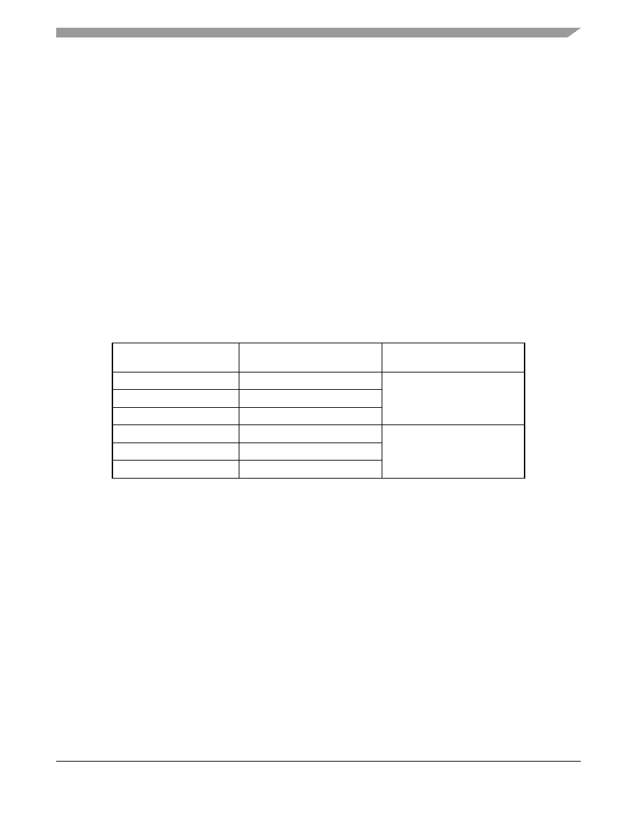
MC68HC908LB8 Data Sheet, Rev. 0
Freescale Semiconductor
229
Chapter 21
Ordering Information and Mechanical Specifications
21.1 Introduction
This section provides ordering information for the MC68HC908GZ8 along with the dimensions for:
∑
20-pin small outline intergrated circuit (SOIC) -- case 751D
∑
20-pin plastic dual in-line package (PDIP) -- case 738
The following figures show the latest package drawings at the time of this publication. To make sure that
you have the latest package specifications, contact your local Freescale Semiconductor Sales Office.
21.2 MC Order Numbers
Table 21-1. MC Order Numbers
MC Order
Number
Operating
Temperature Range
Package
MC68HC908LB8CDWE
≠40∞C to +85∞C
20-pin Small outline
integrated circuit
(SOIC)
MC68HC908LB8VDWE
≠40∞C to +105∞C
MC68HC908LB8MDWE
≠40∞C to +125∞C
MC68HC908LB8CPE
≠40∞C to +85∞C
20-pin Plastic
dual In-line package
(PDIP)
MC68HC908LB8VPE
≠40∞C to +105∞C
MC68HC908LB8MPE
≠40∞C to +125∞C
Temperature and package designators:
C = ≠40∞C to +85∞C
V = ≠40∞C to +105∞C
M = ≠40∞C to +125∞C
DW = Small outline integrated circuit package (SOIC)
E = Leadfree
P = Plastic dual in-line package (PDIP)

Ordering Information and Mechanical Specifications
MC68HC908LB8 Data Sheet, Rev. 0
230
Freescale Semiconductor
21.3 20-Pin Small Outline Integrated Circuit (SOIC) Package -- Case #751D
21.4 20-Pin Plastic Dual In-Line Package (PDIP) -- Case #738
MIN
MIN
MAX
MAX
MILLIMETERS
INCHES
DIM
A
B
C
D
F
G
J
K
M
P
R
0.510
0.299
0.104
0.019
0.035
0.012
0.009
7∞
0.415
0.029
0.499
0.292
0.093
0.014
0.020
0.010
0.004
0∞
0.395
0.010
12.95
7.60
2.65
0.49
0.90
0.32
0.25
7∞
10.55
0.75
12.65
7.40
2.35
0.35
0.50
0.25
0.10
0∞
10.05
0.25
NOTES:
1. DIMENSIONING AND TOLERANCING PER
ANSI Y14.5M, 1982.
2. CONTROLLING DIMENSION: MILLIMETER.
3. DIMENSIONS A AND B DO NOT INCLUDE
MOLD PROTRUSION.
4. MAXIMUM MOLD PROTRUSION 0.150
(0.006) PER SIDE.
5. DIMENSION D DOES NOT INCLUDE
DAMBAR PROTRUSION. ALLOWABLE
DAMBAR PROTRUSION SHALL BE 0.13
(0.005) TOTAL IN EXCESS OF D DIMENSION
AT MAXIMUM MATERIAL CONDITION.
1.27 BSC
0.050 BSC
-A-
-B-
P
10 PL
1
10
11
20
-T-
D
20 PL
K
C
SEATING
PLANE
R
X 45
∞
M
0.010 (0.25)
B
M
M
0.010 (0.25)
T A
B
M
S
S
G
18 PL
F
J
1.070
0.260
0.180
0.022
0.070
0.015
0.140
15∞
0.040
1.010
0.240
0.150
0.015
0.050
0.008
0.110
0∞
0.020
25.66
6.10
3.81
0.39
1.27
0.21
2.80
0∞
0.51
27.17
6.60
4.57
0.55
1.77
0.38
3.55
15∞
1.01
0.050 BSC
0.100 BSC
0.300 BSC
1.27 BSC
2.54 BSC
7.62 BSC
MIN
MIN
MAX
MAX
INCHES
MILLIMETERS
DIM
A
B
C
D
E
F
G
J
K
L
M
N
NOTES:
1. DIMENSIONING AND TOLERANCING PER ANSI
Y14.5M, 1982.
2. CONTROLLING DIMENSION: INCH.
3. DIMENSION L TO CENTER OF LEAD WHEN
FORMED PARALLEL.
4. DIMENSION B DOES NOT INCLUDE MOLD
FLASH.
-A-
C
K
N
E
G
F
D
20 PL
J
20 PL
L
M
-T-
SEATING
PLANE
1
10
11
20
0.25 (0.010)
T A
M
M
0.25 (0.010)
T B
M
M
B


How to Reach Us:
Home Page:
www.freescale.com
E-mail:
support@freescale.com
USA/Europe or Locations Not Listed:
Freescale Semiconductor
Technical Information Center, CH370
1300 N. Alma School Road
Chandler, Arizona 85224
+1-800-521-6274 or +1-480-768-2130
support@freescale.com
Europe, Middle East, and Africa:
Freescale Halbleiter Deutschland GmbH
Technical Information Center
Schatzbogen 7
81829 Muenchen, Germany
+44 1296 380 456 (English)
+46 8 52200080 (English)
+49 89 92103 559 (German)
+33 1 69 35 48 48 (French)
support@freescale.com
Japan:
Freescale Semiconductor Japan Ltd.
Headquarters
ARCO Tower 15F
1-8-1, Shimo-Meguro, Meguro-ku,
Tokyo 153-0064, Japan
0120 191014 or +81 3 5437 9125
support.japan@freescale.com
Asia/Pacific:
Freescale Semiconductor Hong Kong Ltd.
Technical Information Center
2 Dai King Street
Tai Po Industrial Estate
Tai Po, N.T., Hong Kong
+800 2666 8080
support.asia@freescale.com
For Literature Requests Only:
Freescale Semiconductor Literature Distribution Center
P.O. Box 5405
Denver, Colorado 80217
1-800-441-2447 or 303-675-2140
Fax: 303-675-2150
LDCForFreescaleSemiconductor@hibbertgroup.com
Information in this document is provided solely to enable system and
software implementers to use Freescale Semiconductor products. There are
no express or implied copyright licenses granted hereunder to design or
fabricate any integrated circuits or integrated circuits based on the
information in this document.
Freescale Semiconductor reserves the right to make changes without further
notice to any products herein. Freescale Semiconductor makes no warranty,
representation or guarantee regarding the suitability of its products for any
particular purpose, nor does Freescale Semiconductor assume any liability
arising out of the application or use of any product or circuit, and specifically
disclaims any and all liability, including without limitation consequential or
incidental damages. "Typical" parameters that may be provided in Freescale
Semiconductor data sheets and/or specifications can and do vary in different
applications and actual performance may vary over time. All operating
parameters, including "Typicals", must be validated for each customer
application by customer's technical experts. Freescale Semiconductor does
not convey any license under its patent rights nor the rights of others.
Freescale Semiconductor products are not designed, intended, or authorized
for use as components in systems intended for surgical implant into the body,
or other applications intended to support or sustain life, or for any other
application in which the failure of the Freescale Semiconductor product could
create a situation where personal injury or death may occur. Should Buyer
purchase or use Freescale Semiconductor products for any such unintended
or unauthorized application, Buyer shall indemnify and hold Freescale
Semiconductor and its officers, employees, subsidiaries, affiliates, and
distributors harmless against all claims, costs, damages, and expenses, and
reasonable attorney fees arising out of, directly or indirectly, any claim of
personal injury or death associated with such unintended or unauthorized
use, even if such claim alleges that Freescale Semiconductor was negligent
regarding the design or manufacture of the part.
FreescaleTM and the Freescale logo are trademarks of Freescale
Semiconductor, Inc. All other product or service names are the property
of their respective owners. The ARM POWERED logo is a registered
trademark of ARM Limited. ARM7TDMI-S is a trademark of ARM Limited.
Java and all other Java-based marks are trademarks or registered
trademarks of Sun Microsystems, Inc. in the U.S. and other countries.
The Bluetooth trademarks are owned by their proprietor and used by
Freescale Semiconductor, Inc. under license.
© Freescale Semiconductor, Inc. 2005. All rights reserved.
MC68HC908LB8
Rev. 0
2/2005
