
Motorola reserves the right to make changes without further notice to any products herein to improve reliability, function or
design. Motorola does not assume any liability arising out of the application or use of any product or circuit described herein;
neither does it convey any license under its patent rights nor the rights of others. Motorola products are not designed, intended,
or authorized for use as components in systems intended for surgical implant into the body, or other applications intended to
support or sustain life, or for any other application in which the failure of the Motorola product could create a situation where
personal injury or death may occur. Should Buyer purchase or use Motorola products for any such unintended or unauthorized
application, Buyer shall indemnify and hold Motorola and its officers, employees, subsidiaries, affiliates, and distributors harmless
against all claims, costs, damages, and expenses, and reasonable attorney fees arising out of, directly or indirectly, any claim of
personal injury or death associated with such unintended or unauthorized use, even if such claim alleges that Motorola was
negligent regarding the design or manufacture of the part.
DOCUMENT NUMBER
S12FTS128KV1/D
1
FTS128K
Block Guide
V01.03
Original Release Date: 19 JUL 2001
Revised: 11 MAR 2002
Motorola, Inc
F
r
e
e
s
c
a
l
e
S
e
m
i
c
o
n
d
u
c
t
o
r
,
I
Freescale Semiconductor, Inc.
For More Information On This Product,
Go to: www.freescale.com
n
c
.
.
.
Block Guide -- S12FTS128KV1/D V01.03
2
Revision History
Version
Number
Revision
Date
Effective
Date
Author
Description of Changes
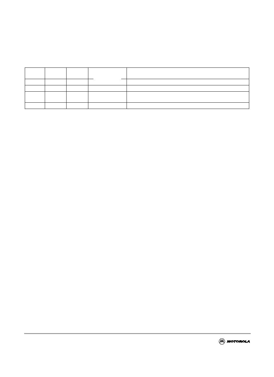
V01.00
19JUL01
19JUL01
Derek Beattie
Initial Version.
V01.01
04SEP01
04SEP01
Derek Beattie
Correct Table3_2: Memory Map Summary
V01.02
23NOV01
23NOV01
Sahba Aazami
Add description of WRALL bit in FTSTMOD register.
Add description of FADDR and FDATA registers.
V01.03
11MAR02 11MAR02
Brian Cook
Modify document number.
F
r
e
e
s
c
a
l
e
S
e
m
i
c
o
n
d
u
c
t
o
r
,
I
Freescale Semiconductor, Inc.
For More Information On This Product,
Go to: www.freescale.com
n
c
.
.
.

Block Guide -- FTS128K V01.03
3
Table of Contents
Section 1 Introduction
1.1
Overview. . . . . . . . . . . . . . . . . . . . . . . . . . . . . . . . . . . . . . . . . . . . . . . . . . . . . . . . . . . . . .9
1.1.1
Glossary . . . . . . . . . . . . . . . . . . . . . . . . . . . . . . . . . . . . . . . . . . . . . . . . . . . . . . . . . . . .9
1.2
Features . . . . . . . . . . . . . . . . . . . . . . . . . . . . . . . . . . . . . . . . . . . . . . . . . . . . . . . . . . . . . .9
1.3
Modes of Operation . . . . . . . . . . . . . . . . . . . . . . . . . . . . . . . . . . . . . . . . . . . . . . . . . . . .10
1.4
Block Diagram . . . . . . . . . . . . . . . . . . . . . . . . . . . . . . . . . . . . . . . . . . . . . . . . . . . . . . . .11
Section 2 External Signal Description
2.1
Overview. . . . . . . . . . . . . . . . . . . . . . . . . . . . . . . . . . . . . . . . . . . . . . . . . . . . . . . . . . . . .13
Section 3 Memory Map and Registers
3.1
Overview. . . . . . . . . . . . . . . . . . . . . . . . . . . . . . . . . . . . . . . . . . . . . . . . . . . . . . . . . . . . .15
3.2
Modules Memory Map . . . . . . . . . . . . . . . . . . . . . . . . . . . . . . . . . . . . . . . . . . . . . . . . . .15
3.3
Register Descriptions . . . . . . . . . . . . . . . . . . . . . . . . . . . . . . . . . . . . . . . . . . . . . . . . . . .20
3.3.1
FCLKDIV -- Flash Clock Divider Register . . . . . . . . . . . . . . . . . . . . . . . . . . . . . . . . .21
3.3.2
FSEC -- Flash Security Register. . . . . . . . . . . . . . . . . . . . . . . . . . . . . . . . . . . . . . . .21
3.3.3
FTSTMOD -- Flash Test Mode Register . . . . . . . . . . . . . . . . . . . . . . . . . . . . . . . . . .22
3.3.4
FCNFG -- Flash Configuration Register . . . . . . . . . . . . . . . . . . . . . . . . . . . . . . . . . .23
3.3.5
FPROT -- Flash Protection Register . . . . . . . . . . . . . . . . . . . . . . . . . . . . . . . . . . . . .24
3.3.6
FSTAT -- Flash Status Register . . . . . . . . . . . . . . . . . . . . . . . . . . . . . . . . . . . . . . . .26
3.3.7
FCMD -- Flash Command Register . . . . . . . . . . . . . . . . . . . . . . . . . . . . . . . . . . . . .27
3.3.8
RESERVED1 . . . . . . . . . . . . . . . . . . . . . . . . . . . . . . . . . . . . . . . . . . . . . . . . . . . . . . .28
3.3.9
FADDR -- 16-bit Address Register . . . . . . . . . . . . . . . . . . . . . . . . . . . . . . . . . . . . . .28
3.3.10
FDATA -- Flash 16-bit Data Buffer and Register . . . . . . . . . . . . . . . . . . . . . . . . . . .29
Section 4 Functional Description
4.1
Program and Erase Operation . . . . . . . . . . . . . . . . . . . . . . . . . . . . . . . . . . . . . . . . . . . .31
4.1.1
Writing the FCLKDIV Register . . . . . . . . . . . . . . . . . . . . . . . . . . . . . . . . . . . . . . . . . .31
4.1.2
Program and Erase Sequences in User Mode. . . . . . . . . . . . . . . . . . . . . . . . . . . . . .34
4.1.3
Valid Flash Commands . . . . . . . . . . . . . . . . . . . . . . . . . . . . . . . . . . . . . . . . . . . . . . .36
4.1.4
Illegal Flash Operations . . . . . . . . . . . . . . . . . . . . . . . . . . . . . . . . . . . . . . . . . . . . . . .36
4.2
Wait Mode . . . . . . . . . . . . . . . . . . . . . . . . . . . . . . . . . . . . . . . . . . . . . . . . . . . . . . . . . . .37
4.3
Stop Mode . . . . . . . . . . . . . . . . . . . . . . . . . . . . . . . . . . . . . . . . . . . . . . . . . . . . . . . . . . .37
F
r
e
e
s
c
a
l
e
S
e
m
i
c
o
n
d
u
c
t
o
r
,
I
Freescale Semiconductor, Inc.
For More Information On This Product,
Go to: www.freescale.com
n
c
.
.
.

Block Guide -- FTS128K V01.03
4
4.4
Background Debug Mode. . . . . . . . . . . . . . . . . . . . . . . . . . . . . . . . . . . . . . . . . . . . . . . .38
4.5
Flash Security. . . . . . . . . . . . . . . . . . . . . . . . . . . . . . . . . . . . . . . . . . . . . . . . . . . . . . . . .38
4.5.1
Unsecuring the Flash via the Backdoor Key Access . . . . . . . . . . . . . . . . . . . . . . . . .38
Section 5 Resets
5.1
General. . . . . . . . . . . . . . . . . . . . . . . . . . . . . . . . . . . . . . . . . . . . . . . . . . . . . . . . . . . . . .41
Section 6 Interrupts
6.1
General. . . . . . . . . . . . . . . . . . . . . . . . . . . . . . . . . . . . . . . . . . . . . . . . . . . . . . . . . . . . . .43
6.2
Description of Interrupt Operation . . . . . . . . . . . . . . . . . . . . . . . . . . . . . . . . . . . . . . . . .43
F
r
e
e
s
c
a
l
e
S
e
m
i
c
o
n
d
u
c
t
o
r
,
I
Freescale Semiconductor, Inc.
For More Information On This Product,
Go to: www.freescale.com
n
c
.
.
.

Block Guide -- FTS128K V01.03
5
List of Figures
Figure 1-1
FTS128K Module Block Diagram . . . . . . . . . . . . . . . . . . . . . . . . . . . . . . . . . . . .11
Figure 3-1
FTS128K Flash Memory Map . . . . . . . . . . . . . . . . . . . . . . . . . . . . . . . . . . . . . . .17
Figure 3-2
Flash Clock Divider Register (FCLKDIV). . . . . . . . . . . . . . . . . . . . . . . . . . . . . . .21
Figure 3-3
Flash Security Register (FSEC). . . . . . . . . . . . . . . . . . . . . . . . . . . . . . . . . . . . . .22
Figure 3-4
fts128k Test Mode Register (FTSTMOD) . . . . . . . . . . . . . . . . . . . . . . . . . . . . . .22
Figure 3-5
Flash Configuration Register (FCNFG) . . . . . . . . . . . . . . . . . . . . . . . . . . . . . . . .23
Figure 3-6
Flash Protection Register (FPROT). . . . . . . . . . . . . . . . . . . . . . . . . . . . . . . . . . .24
Figure 3-7
Flash Status Register (FSTAT) . . . . . . . . . . . . . . . . . . . . . . . . . . . . . . . . . . . . . .26
Figure 3-8
Flash Command Buffer and Register (FCMD). . . . . . . . . . . . . . . . . . . . . . . . . . .27
Figure 3-9
RESERVED1 . . . . . . . . . . . . . . . . . . . . . . . . . . . . . . . . . . . . . . . . . . . . . . . . . . . .28
Figure 3-10 fts128k: Flash 8-bit Address High Register (FADDRHI) . . . . . . . . . . . . . . . . . . .28
Figure 3-11 Flash 8-bit Address Low Register (FADDRLO) . . . . . . . . . . . . . . . . . . . . . . . . . .28
Figure 3-12 8-bit Flash Data High Register (FDATAHI) . . . . . . . . . . . . . . . . . . . . . . . . . . . . .29
Figure 3-13 8-bit Flash Data Low Register (FDATALO) . . . . . . . . . . . . . . . . . . . . . . . . . . . . .29
Figure 4-1
PRDIV8 and FDIV bits Determination Procedure . . . . . . . . . . . . . . . . . . . . . . . .33
Figure 4-2
Example Program Algorithm . . . . . . . . . . . . . . . . . . . . . . . . . . . . . . . . . . . . . . . .35
Figure 6-1
FTS128K Flash Interrupt Implementation . . . . . . . . . . . . . . . . . . . . . . . . . . . . . .44
F
r
e
e
s
c
a
l
e
S
e
m
i
c
o
n
d
u
c
t
o
r
,
I
Freescale Semiconductor, Inc.
For More Information On This Product,
Go to: www.freescale.com
n
c
.
.
.

Block Guide -- FTS128K V01.03
6
F
r
e
e
s
c
a
l
e
S
e
m
i
c
o
n
d
u
c
t
o
r
,
I
Freescale Semiconductor, Inc.
For More Information On This Product,
Go to: www.freescale.com
n
c
.
.
.

Block Guide -- FTS128K V01.03
7
List of Tables
Table 3-1
Flash Protection/Options Field. . . . . . . . . . . . . . . . . . . . . . . . . . . . . . . . . . . . . . .18
Table 3-2
Memory Maps Summary . . . . . . . . . . . . . . . . . . . . . . . . . . . . . . . . . . . . . . . . . . .18
Table 3-3
FTS128K Memory Map . . . . . . . . . . . . . . . . . . . . . . . . . . . . . . . . . . . . . . . . . . . .20
Table 3-4
Security States. . . . . . . . . . . . . . . . . . . . . . . . . . . . . . . . . . . . . . . . . . . . . . . . . . .22
Table 3-5
Register Bank Selects . . . . . . . . . . . . . . . . . . . . . . . . . . . . . . . . . . . . . . . . . . . . .24
Table 3-6
Loading of the Protection Register from Flash . . . . . . . . . . . . . . . . . . . . . . . . . .24
Table 3-7
Flash Higher Address Range Protection . . . . . . . . . . . . . . . . . . . . . . . . . . . . . . .25
Table 3-8
Flash Lower Address Range Protection . . . . . . . . . . . . . . . . . . . . . . . . . . . . . . .25
Table 3-9
FCMD NVM User Mode Commands . . . . . . . . . . . . . . . . . . . . . . . . . . . . . . . . . .27
Table 4-1
Valid Flash Commands . . . . . . . . . . . . . . . . . . . . . . . . . . . . . . . . . . . . . . . . . . . .36
Table 6-1
Flash Interrupt Sources . . . . . . . . . . . . . . . . . . . . . . . . . . . . . . . . . . . . . . . . . . . .43
F
r
e
e
s
c
a
l
e
S
e
m
i
c
o
n
d
u
c
t
o
r
,
I
Freescale Semiconductor, Inc.
For More Information On This Product,
Go to: www.freescale.com
n
c
.
.
.

Block Guide -- FTS128K V01.03
8
F
r
e
e
s
c
a
l
e
S
e
m
i
c
o
n
d
u
c
t
o
r
,
I
Freescale Semiconductor, Inc.
For More Information On This Product,
Go to: www.freescale.com
n
c
.
.
.

Block Guide -- FTS128K V01.03
9
Section 1 Introduction
1.1 Overview
This document describes the FTS128K module which is a 128k byte Flash (Non-Volatile) Memory. The
Flash array is organized as 2 blocks of 64k bytes. Each block is organized as 1024 rows of 64 bytes. The
Flash block's erase sector size is 8 rows (512 bytes).
The Flash memory may be read as either bytes, aligned words or misaligned words. Read access time is
one bus cycle for byte and aligned word, and two bus cycles for misaligned words.
Program and erase functions are controlled by a command driven interface. Both sector erase and mass
erase of an entire 64k byte Flash block are supported. An erased bit reads '1' and a programmed bit reads
'0'. The high voltage required to program and erase is generated internally by on-chip charge pumps.
Both Flash blocks can be programmed or erased at the same time, however it is not possible to read from
a Flash block while it is being erased or programmed.
The Flash is ideal for program and data storage for single-supply applications allowing for field
reprogramming without requiring external programming voltage sources.
WARNING
A word must be erased before being programmed. Cumulative programming of bits within a word
is not allowed.
1.1.1 Glossary
Banked Register
A register operating on one Flash block which shares the same register address as the equivalent registers
for the other Flash block. The active register bank is selected by a bank-select bit in the unbanked register
space.
Common Register
A register which operates on both Flash blocks.
Command Sequence
A three-step MCU instruction sequence to program, erase or erase-verify a Flash block.
1.2 Features
∑
128k bytes of flash memory comprising two 64k byte blocks.
∑
Each block in the Flash module can be read, programmed or erased concurrently.
F
r
e
e
s
c
a
l
e
S
e
m
i
c
o
n
d
u
c
t
o
r
,
I
Freescale Semiconductor, Inc.
For More Information On This Product,
Go to: www.freescale.com
n
c
.
.
.

Block Guide -- FTS128K V01.03
10
∑
Automated program and erase algorithm.
∑
Interrupts on Flash command completion and command buffer empty.
∑
Fast sector erase and word program operation.
∑
2-stage command pipeline.
∑
Flexible protection scheme for protection against accidental program or erase.
∑
Single power supply program and erase.
∑
Security feature.
1.3 Modes of Operation
∑
Program and erase operation (please refer to
4.1
for details).
F
r
e
e
s
c
a
l
e
S
e
m
i
c
o
n
d
u
c
t
o
r
,
I
Freescale Semiconductor, Inc.
For More Information On This Product,
Go to: www.freescale.com
n
c
.
.
.
Block Guide -- FTS128K V01.03
11
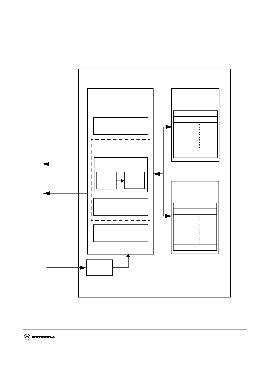
1.4 Block Diagram
Figure 1-1
shows a block diagram of the FTS128K module.
Figure 1-1 FTS128K Module Block Diagram
FTS128K
Flash-0 Array
32k * 16 Bits
row0
row1
row1024
Oscillator
Clock
Divider
Clock
Command
Interface
Command Pipelines
comm2
Command
Complete
Interrupt
Command
Buffer Empty
Interrupt
Common
EECLK
addr2
data2
comm1
addr1
data1
Flash 0-1
Registers
Banked
Registers
Protection
Security
Flash-1 Array
32k * 16 Bits
row0
row1
row1024
F
r
e
e
s
c
a
l
e
S
e
m
i
c
o
n
d
u
c
t
o
r
,
I
Freescale Semiconductor, Inc.
For More Information On This Product,
Go to: www.freescale.com
n
c
.
.
.

Block Guide -- FTS128K V01.03
12
F
r
e
e
s
c
a
l
e
S
e
m
i
c
o
n
d
u
c
t
o
r
,
I
Freescale Semiconductor, Inc.
For More Information On This Product,
Go to: www.freescale.com
n
c
.
.
.

Block Guide -- FTS128K V01.03
13
Section 2 External Signal Description
2.1 Overview
The FTS128K module contains no signals that connect off-chip.
F
r
e
e
s
c
a
l
e
S
e
m
i
c
o
n
d
u
c
t
o
r
,
I
Freescale Semiconductor, Inc.
For More Information On This Product,
Go to: www.freescale.com
n
c
.
.
.

Block Guide -- FTS128K V01.03
14
F
r
e
e
s
c
a
l
e
S
e
m
i
c
o
n
d
u
c
t
o
r
,
I
Freescale Semiconductor, Inc.
For More Information On This Product,
Go to: www.freescale.com
n
c
.
.
.

Block Guide -- FTS128K V01.03
15
Section 3 Memory Map and Registers
3.1 Overview
This section describes the FTS128K memory maps and registers.
3.2 Modules Memory Map
Figure 3-1
shows the FTS128K memory map. The HCS12 architecture places the Flash memory address
between $4000 and $FFFF, which corresponds to three 16k byte pages.The content of the PPAGE register
is used to map the logical middle page ranging from address $8000 to $BFFF to any physical 16K bytes
page in the physical memory
1
Shown within the blocks are a protection/options field and user defined
Flash protected sectors.
The FPOPEN bit in the FPROT register (see
3.3.5
) can globally protect the entirety of the corresponding
memory block. However for both Flash blocks, two protected areas, one starting from the Flash page
starting address (called lower) towards higher addresses and the other one growing downward from the
Flash page end address (called higher) can be activated. For Flash 0, the latter is mainly targeted to hold
the boot loader code since it covers the vector space. All the other areas may be used to keep critical
parameters.
The pagination process using the PPAGE register is handled the HCS12 CPU.
The Flash module register space covers the addresses BASE + $100 to BASE + $10F.
NOTES
:
1. By placing $3F or $3E in the PPAGE register, the bottom respectively top "fixed" 16Kbytes pages can be seen twice in the
MCU memory map.
F
r
e
e
s
c
a
l
e
S
e
m
i
c
o
n
d
u
c
t
o
r
,
I
Freescale Semiconductor, Inc.
For More Information On This Product,
Go to: www.freescale.com
n
c
.
.
.

Block Guide -- FTS128K V01.03
16
Security information that allows the MCU to prevent intrusive access to the NVM module is stored in the
Flash block's Flash Protection/Options field. This special memory field is held in Flash block 0. A
description of the 16 bytes used in this field is given in
Table 3-1
.
F
r
e
e
s
c
a
l
e
S
e
m
i
c
o
n
d
u
c
t
o
r
,
I
Freescale Semiconductor, Inc.
For More Information On This Product,
Go to: www.freescale.com
n
c
.
.
.

Block Guide -- FTS128K V01.03
17
Figure 3-1 FTS128K Flash Memory Map
Flash Control Registers
(BASE + $100)
$FF00 - $FF0F, Flash Protection/Security Field
(BASE + $10F)
$8000
(16 bytes)
Flash Protected Low Sectors
0.5K, 1K, 2K, 4K bytes
FLASH_START = $4000
$4800
$4200
$4400
$5000
12K
16K PAGED
MEMORY
$38
$39
$3A
$3B
$3E
$3C
$3D
$3E
$3F
Two Blocks of Flash IP
Note: $38-$3F correspond to the PPAGE register content
FLASH_END = $FFFF
$F800
$F000
$C000
$E000
Flash Protected High Sectors
2K, 4K, 8K, 16K bytes
$3F
Block 0
Block 1
F
r
e
e
s
c
a
l
e
S
e
m
i
c
o
n
d
u
c
t
o
r
,
I
Freescale Semiconductor, Inc.
For More Information On This Product,
Go to: www.freescale.com
n
c
.
.
.

Block Guide -- FTS128K V01.03
18
Table 3-1 Flash Protection/Options Field
Address
Size
(bytes)
Description
$FF00 - $FF07
8
Backdoor Comparison Keys
$FF08 - $FF0B
4
Reserved
$FF0C
1
Block 1 Flash Protection byte
Refer to Section 3.3.5
$FF0D
1
Block 0 Flash Protection byte
Refer to Section 3.3.5
$FF0E
1
Reserved
$FF0F
1
Flash Options/Security byte
Refer to Section 3.3.2
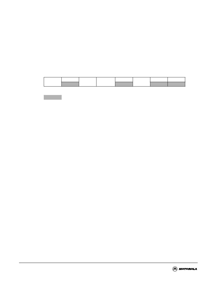
Table 3-2 Memory Maps Summary
MCU
Address
Range
PPAGE
Protectable
Low Range
Protectable
High Range
Flash
Block
Block
Relative
Address
1
$4000-$7FFF
Unpaged
($3E)
$4000-$41FF
N.A.
0
$8000-$BFFF
$4000-$43FF
$4000-$47FF
$4000-$4FFF
F
r
e
e
s
c
a
l
e
S
e
m
i
c
o
n
d
u
c
t
o
r
,
I
Freescale Semiconductor, Inc.
For More Information On This Product,
Go to: www.freescale.com
n
c
.
.
.

Block Guide -- FTS128K V01.03
19
$8000-$BFFF
$38
N.A.
N.A.
1
$0000-$3FFF
$39
N.A.
N.A.
$4000-$7FFF
$3A
$8000-$81FF
N.A.
$8000-$BFFF
$8000-$83FF
$8000-$87FF
$8000-$8FFF
$3B
N.A.
$B800-$BFFF
$C000-$FFFF
$B000-$BFFF
$A000-$BFFF
$8000-$BFFF
$3C
N.A.
N.A.
0
$0000-$3FFF
$3D
N.A.
N.A.
$4000-$7FFF
$3E
$8000-$81FF
N.A.
$8000-$BFFF
$8000-$83FF
$8000-$87FF
$8000-$8FFF
$3F
N.A.
$B800-$BFFF
$C000-$FFFF
$B000-$BFFF
$A000-$BFFF
$8000-$BFFF
$C000-$FFFF
Unpaged
($3F)
N.A.
$F800-$FFFF
0
$C000-$FFFF
$F000-$FFFF
$E000-$FFFF
$C000-$FFFF
NOTES
:
1. Inside each Flash block of size 64 Kbyte.
Table 3-2 Memory Maps Summary
MCU
Address
Range
PPAGE
Protectable
Low Range
Protectable
High Range
Flash
Block
Block
Relative
Address
1
F
r
e
e
s
c
a
l
e
S
e
m
i
c
o
n
d
u
c
t
o
r
,
I
Freescale Semiconductor, Inc.
For More Information On This Product,
Go to: www.freescale.com
n
c
.
.
.

Block Guide -- FTS128K V01.03
20
The Flash module has hardware interlocks which protect data from accidental corruption. One protected
sector is located at the higher address end of Flash block 0, just below $FFFF. Another protected sector is
located at the lower address end of Flash block 0, just after the beginning of the Flash code implementation
at address $4000. Both the high and low address protected sectors in the Flash can be sized from 512 bytes
to 4K bytes. The middle Flash page can also exhibit protectable areas as indicated in the memory map
summary
Table 3-2
.
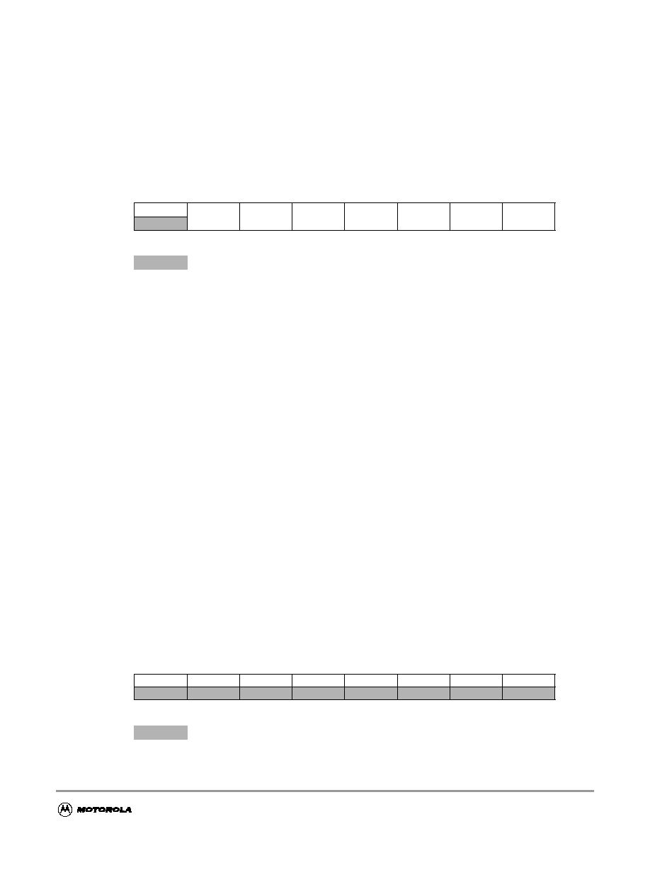
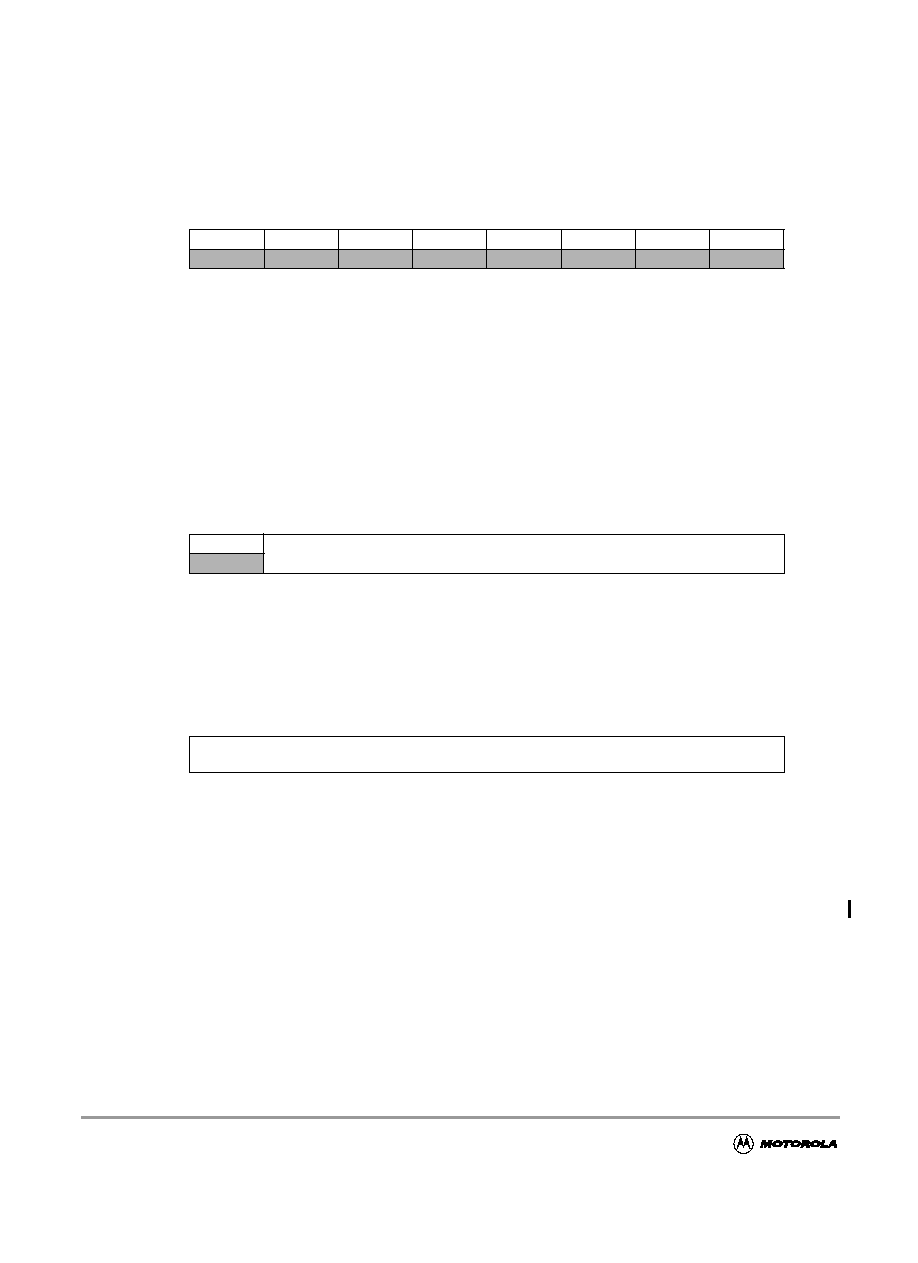
The NVM module also contains a set of 16 control and status registers located in address space BASE +
$100 to BASE + $10F. In order to accommodate two Flash blocks with a minimum register address space,
a set of registers (BASE+$104 to BASE+$10B) is duplicated in two banks. The active bank is selected by
the BKSEL bit in the unbanked Flash Configuration Register (FCNFG). A summary of these registers is
given in
Table 3-3
.
NOTE:
Register Address = Base Address + Address Offset, where the Base Address is
defined at the MCU level and the Address Offset is defined at the module level.
3.3 Register Descriptions
NOTE
Table 3-3 FTS128K Memory Map
Address
Offset
Use
Access
$_00
Flash Clock Divider Register (FCLKDIV)
R/W
$_01
Flash Security Register (FSEC)
R
$_02
Flash Test Mode Register (FTSTMOD)
1
NOTES
:
1. Intended for factory test purposes only.
R
$_03
Flash Configuration Register (FCNFG)
R/W
$_04
Flash Protection Register (FPROT)
R/W
$_05
Flash Status Register (FSTAT)
R/W
$_06
Flash Command Register (FCMD)
R/W
$_07
RESERVED1
2
2. RESERVED1 intended for factory test purposes only.
R
$_08
16-bit Address Register (FADDRHI)
3
3. Intended for factory test purposes only.
R
$_09
16-bit Address Register (FADDRLO)
4
4. Intended for factory test purposes only.
R
$_0A
16-bit Data Register (FDATAHI)
5
5. Intended for factory test purposes only.
R
$_0B
16-bit Data Register (FDATALO)
6
6. Intended for factory test purposes only.
R
F
r
e
e
s
c
a
l
e
S
e
m
i
c
o
n
d
u
c
t
o
r
,
I
Freescale Semiconductor, Inc.
For More Information On This Product,
Go to: www.freescale.com
n
c
.
.
.
Block Guide -- FTS128K V01.03
21
3.3.1 FCLKDIV -- Flash Clock Divider Register
The FCLKDIV register is used to control timed events in program and erase algorithms. This register is
unbanked.
Figure 3-2 Flash Clock Divider Register (FCLKDIV)
All bits in the FCLKDIV register are readable, bits 6-0 are write once and bit 7 is not writable.
FDIVLD -- Clock Divider Loaded.
1 = Register has been written to since the last reset.
0 = Register has not been written.
PRDIV8 -- Enable Prescaler by 8.
1 = Enables a prescaler by 8, to divide the Flash module input oscillator clock before feeding into
the CLKDIV divider.
0 = The input oscillator clock is directly fed into the FCLKDIV divider.
FDIV[5:0] -- Clock Divider Bits.
The combination of PRDIV8 and FDIV[5:0] effectively divides the Flash module input oscillator
clock down to a frequency of 150kHz - 200kHz. The maximum divide ratio is 512. Please refer to
section
4.1.1
for more information.
3.3.2 FSEC -- Flash Security Register
This FSEC register holds all bits associated with the device security. This register is unbanked.
Register address BASE + $100
7
6
5
4
3
2
1
0
R
FDIVLD
PRDIV8
FDIV5
FDIV4
FDIV3
FDIV2
FDIV1
FDIV0
W
RESET:
0
0
0
0
0
0
0
0
= Unimplemented or Reserved
Register address BASE + $101
7
6
5
4
3
2
1
0
R
KEYEN
NV6
NV5
NV4
NV3
NV2
SEC1
SEC0
W
Reset:
F
F
F
F
F
F
F
F
= Unimplemented or Reserved
F
r
e
e
s
c
a
l
e
S
e
m
i
c
o
n
d
u
c
t
o
r
,
I
Freescale Semiconductor, Inc.
For More Information On This Product,
Go to: www.freescale.com
n
c
.
.
.

Block Guide -- FTS128K V01.03
22
Figure 3-3 Flash Security Register (FSEC)
All bits in the FSEC register are readable but not writable.
The FSEC register is loaded from the Flash Protection/Options field byte at $FF0F during the reset
sequence, indicated by "F" in
Figure 3-3
.
KEYEN -- Enable backdoor key to security.
1 = backdoor to Flash is enabled.
0 = backdoor to Flash is disabled.
NV[6:2] -- Non Volatile Flag Bits.
These 5 bits are available to the user as non-volatile flags.
SEC[1:0] -- Memory Security Bits.
The SEC[1:0] bits define the security state of the device as shown in
Table 3-4
. If the Flash is
unsecured using the Backdoor Key Access, the SEC bits are forced to 10.
The security function in the Flash module is described in section
4.5
.
3.3.3 FTSTMOD -- Flash Test Mode Register
The unbanked FTSTMOD register is used primarily to control the NVM Test modes.
Figure 3-4 fts128k Test Mode Register (FTSTMOD)
Table 3-4 Security States
SEC[1:0]
Description
00
secured
01
secured
10
unsecured
11
secured
Register address BASE + $102
7
6
5
4
3
2
1
0
R
N/A
N/A
N/A
WRALL
0
0
0
N/A
W
Reset:
0
0
0
0
0
0
0
0
= Unimplemented or Reserved
F
r
e
e
s
c
a
l
e
S
e
m
i
c
o
n
d
u
c
t
o
r
,
I
Freescale Semiconductor, Inc.
For More Information On This Product,
Go to: www.freescale.com
n
c
.
.
.

Block Guide -- FTS128K V01.03
23
In user modes, all bits in the FTSTMOD register read zero and are not writable. The WRALL bit is
writable only in special modes. The purpose of this bit is to launch a command on all blocks in parallel.
This can be useful for mass erase and blank check operations. All other bits in this register must be written
to zero at all times.
WRALL --Write to all register banks.
If this bit is set, all banked registers sharing the same address will be written simultaneously.
1 = Write to all register banks.
0 = Write only to the bank selected via BKSEL.
3.3.4 FCNFG -- Flash Configuration Register
The FCNFG register enables the Flash interrupts, gates the security backdoor writes and selects the register
bank to be operated on. This register is not banked.
Figure 3-5 Flash Configuration Register (FCNFG)
CBEIE, CCIE, KEYACC and BKSEL are readable and writable. Bits 4-1 read zero and are not writable.
CBEIE -- Command Buffer Empty Interrupt Enable.
The CBEIE bit enables the interrupts in case of an empty command buffer in the Flash.
1 = An interrupt will be requested whenever the CBEIF flag,
Figure 3-7
, is set.
0 = Command Buffer Empty interrupts disabled.
CCIE -- Command Complete Interrupt Enable.
The CCIE bit enables the interrupts in case of all commands being completed in the Flash.
1 = An interrupt will be requested whenever the CCIF,
Figure 3-7
, flag is set.
0 = Command Complete interrupts disabled.
KEYACC -- Enable Security Key Writing.
1 = Writes to Flash array are interpreted as keys to open the backdoor. Reads of the Flash array
return invalid data.
0 = Flash writes are interpreted as the start of a program or erase sequence.
BKSEL -- Register Bank Select
This bit is used to select one of the two register banks. The register bank associated with Flash 0 is the
default out of reset. The bank selection is according to
Table 3-5
.
Register address BASE + $103
7
6
5
4
3
2
1
0
R
CBEIE
CCIE
KEYACC
0
0
0
0
BKSEL
W
Reset:
0
0
0
0
0
0
0
0
= Unimplemented or Reserved
F
r
e
e
s
c
a
l
e
S
e
m
i
c
o
n
d
u
c
t
o
r
,
I
Freescale Semiconductor, Inc.
For More Information On This Product,
Go to: www.freescale.com
n
c
.
.
.
Block Guide -- FTS128K V01.03
24
3.3.5 FPROT -- Flash Protection Register
The FPROT register defines which Flash sectors are protected against program or erase. This register is
banked.
Figure 3-6 Flash Protection Register (FPROT)
The FPROT register is readable in user and special modes. Bit NV6 is not writable. FPOPEN, FPHDIS
and FPLDIS bits in the FPROT register can only be written to the protected state (i.e. 0). FPLS[1:0] can
be written anytime until bit FPLDIS is cleared. FPHS[1:0] bits can be written anytime until bit FPHDIS is
cleared. If the FPOPEN bit is cleared, then the state of the FPHDIS, FPHS[1:0], FPLDIS and FPLS[1:0]
bits is irrelevant. The FPROT register is loaded from the Flash array during reset according to the
following table.
To change the Flash protection that will be loaded on reset, the upper sector of Flash must be unprotected,
then the Flash Protect/Security byte located as described in
Table 3-1
must be written to.
A protected Flash sector is disabled by the bits FPHDIS and FPLDIS while the size of the protected sector
is defined by FPHS[1:0] and FPLS[1:0] in the FPROT register.
Table 3-5 Register Bank Selects
BKSEL
Selected Register
Bank
0
Flash 0
1
Flash 1
Register address BASE + $104
7
6
5
4
3
2
1
0
R
FPOPEN
NV6
FPHDIS
FPHS1
FPHS0
FPLDIS
FPLS1
FPLS0
W
Reset:
F
F
F
F
F
F
F
F
= Unimplemented or Reserved
Table 3-6 Loading of the Protection Register from Flash
Flash Address
Protection byte for
$FF0D
Flash 0
$FF0C
Flash 1
F
r
e
e
s
c
a
l
e
S
e
m
i
c
o
n
d
u
c
t
o
r
,
I
Freescale Semiconductor, Inc.
For More Information On This Product,
Go to: www.freescale.com
n
c
.
.
.

Block Guide -- FTS128K V01.03
25
Trying to alter any of the protected areas will result in a protect violation error and bit PVIOL will be set
in the Flash Status Register FSTAT. A mass erase of a whole Flash block is only possible when protection
is fully disabled by setting FPLDIS and FPHDIS bits.
FPOPEN -- Opens the Flash for program or erase.
1 = The Flash sectors not protected are enabled for program or erase.
0 = The whole Flash array is protected. In this case the FPHDIS, FPHS[1:0], FPLDIS and
FPLS[1:0] bits within the protection register are don't care.
FPHDIS -- Flash Protection Higher address range Disable.
The FPHDIS bit determines whether there is a protected area in the higher space of the Flash address map.
1 = Protection disabled.
0 = Protection enabled.
FPHS[1:0] -- Flash Protection Higher Address Size.
The FPHS[1:0] bits determine the size of the protected sector. Refer to
Table 3-7
.
FPLDIS -- Flash Protection Lower address range Disable.
The FPLDIS bit determines whether there is a protected sector in the lower space of the Flash address map.
1 = Protection disabled.
0 = Protection enabled.
FPLS[1:0] -- Flash Protection Lower Address Size.
The FPLS[1:0] bits determine the size of the protected sector. Refer to
Table 3-8
.
Table 3-7 Flash Higher Address Range Protection
FPHS
Protected
Address
Range
Protected Size
00
see Table 3-2
2K bytes
01
4K
10
8K
11
16K
Table 3-8 Flash Lower Address Range Protection
FPLS
Protected
Address
Range
Protected Size
00
see Table 3-2
512 Bytes
01
1K
10
2K
11
4K
F
r
e
e
s
c
a
l
e
S
e
m
i
c
o
n
d
u
c
t
o
r
,
I
Freescale Semiconductor, Inc.
For More Information On This Product,
Go to: www.freescale.com
n
c
.
.
.
Block Guide -- FTS128K V01.03
26
NV6 -- Non Volatile Flag Bit.
This bit is available as non-volatile flag.
3.3.6 FSTAT -- Flash Status Register
The FSTAT register defines the Flash state machine command status and Flash array access, protection
and blank verify status. This register is banked.
Figure 3-7 Flash Status Register (FSTAT)
Register bits CBEIF, PVIOL and ACCERR are readable and writable, bits CCIF and BLANK are readable
and not writable, bits 3, 1 and 0 read zero and are not writable.
CBEIF -- Command Buffer Empty Interrupt Flag.
The CBEIF flag indicates that the address, data and command buffers are empty so that a new
command sequence can be started. The CBEIF flag is cleared by writing a "1" to CBEIF. Writing a
"0" to the CBEIF flag has no effect on CBEIF but sets ACCERR, which can be used to abort a
command sequence. This bit, CBEIF, is used together with the enable bit CBEIE, to generate the
interrupt request (see also
Figure 6-1
).
1 = Buffers are ready to accept a new command.
0 = Buffers are full.
CCIF -- Command Complete Interrupt Flag.
The CCIF flag indicates that there are no more commands pending. The CCIF flag is cleared when
CBEIF is clear and sets automatically upon completion of all active and pending commands. The CCIF
flag does not set when an active commands completes and a pending command is fetched from the
command buffer. Writing to the CCIF flag has no effect. This bit, CCIF, is used together with the
enable bit CCIE, to generate the interrupt request (see also
Figure 6-1
).
1 = All commands are completed.
0 = Command in progress.
PVIOL -- Protection Violation.
The PVIOL flag indicates an attempt was made to program or erase an address in a protected Flash
memory area. The PVIOL flag is cleared by writing a "1" to PVIOL. Writing a "0" to the PVIOL flag
has no effect on PVIOL. While PVIOL is set in either of the FSTAT registers it is not possible to launch
another command in either of the Flash blocks.
1 = A protection violation has occurred.
0 = No failure.
Register address BASE + $105
7
6
5
4
3
2
1
0
R
CBEIF
CCIF
PVIOL
ACCERR
0
BLANK
0
0
W
Reset:
1
1
0
0
0
0
0
0
= Unimplemented or Reserved
F
r
e
e
s
c
a
l
e
S
e
m
i
c
o
n
d
u
c
t
o
r
,
I
Freescale Semiconductor, Inc.
For More Information On This Product,
Go to: www.freescale.com
n
c
.
.
.

Block Guide -- FTS128K V01.03
27
ACCERR -- Flash Access Error.
The ACCERR flag indicates an illegal access to the selected Flash array. This can be either a violation
of the command sequence, issuing an illegal command (illegal combination of the CMDBx bits in the
FCMD register) or the execution of a CPU STOP instruction while a command is executing (CCIF=0).
The ACCERR flag is cleared by writing a "1" to ACCERR. Writing a "0" to the ACCERR flag has no
effect on ACCERR. While ACCERR is set in either of the FSTAT registers it is not possible to launch
another command in either of the Flash blocks.
1 = Access error has occurred.
0 = No failure.
BLANK -- Array has been verified as erased.
The BLANK flag indicates that an Erase Verify command has checked the Flash block and found it to
be blank. The BLANK flag is cleared by hardware when CBEIF is cleared as part of a new valid
command sequence. Writing to the BLANK flag has no effect on BLANK.
1 = Flash block verifies as erased.
0 = If an Erase Verify command has been requested, and the CCIF flag is set, then a zero in BLANK
indicates the block is not erased.
3.3.7 FCMD -- Flash Command Register
The FCMD register defines the Flash commands. This register is banked.
Figure 3-8 Flash Command Buffer and Register (FCMD)
Bits 7, 4, 3 and 1 read zero and are not writable. Bits CMDB6, CMDB5, CMDB2 and CMDB0 are readable
and writable during a command sequence.
CMDB -- Valid NVM User mode commands are shown in
Table 3-9
. Any commands other than those
mentioned in
Table 3-9
sets the ACCERR bit in the FSTAT register (3.3.6).
Register address BASE + $106
7
6
5
4
3
2
1
0
R
0
CMDB6
CMDB5
0
0
CMDB2
0
CMDB0
W
Reset:
0
0
0
0
0
0
0
0
Table 3-9 FCMD NVM User Mode Commands
Command
Meaning
$05
Erase Verify
$20
Byte Program
$40
Sector Erase
$41
Mass Erase
F
r
e
e
s
c
a
l
e
S
e
m
i
c
o
n
d
u
c
t
o
r
,
I
Freescale Semiconductor, Inc.
For More Information On This Product,
Go to: www.freescale.com
n
c
.
.
.
Block Guide -- FTS128K V01.03
28
3.3.8 RESERVED1
This register is reserved for factory testing and is not accessible to the user. This register is banked.
Register address BASE + $107
Figure 3-9 RESERVED1
All bits read zero and are not writable.
3.3.9 FADDR -- 16-bit Address Register
FADDRHI and FADDRLO are the Flash address registers.
Figure 3-10 fts128k: Flash 8-bit Address High Register (FADDRHI)
Figure 3-11 Flash 8-bit Address Low Register (FADDRLO)
In user modes, the FADDR (FADDRHI, FADDRLO) register reads zeros and is not writable. The unused
bits in register FADDRHI (gray shaded bit positions in
Figure 3-10
) read zero and are not writable.
The FADDRHI and FADDRLO registers can be written in special modes by writing to address BASE +
$108 and BASE + $109 in the register space.
For sector erase, the MCU address bits AB[8:0] are don't care.
For mass erase, any address within the block is valid to start the command.
7
6
5
4
3
2
1
0
R
0
0
0
0
0
0
0
0
W
Reset:
0
0
0
0
0
0
0
0
Register address Base + $108
15
14
13
12
11
10
9
8
R
0
FABHI
W
Reset:
0
0
0
0
0
0
0
0
Register address Base + $109
15
14
13
12
11
10
9
8
R
FABLO
W
Reset:
0
0
0
0
0
0
0
0
F
r
e
e
s
c
a
l
e
S
e
m
i
c
o
n
d
u
c
t
o
r
,
I
Freescale Semiconductor, Inc.
For More Information On This Product,
Go to: www.freescale.com
n
c
.
.
.

Block Guide -- FTS128K V01.03
29
3.3.10 FDATA -- Flash 16-bit Data Buffer and Register
FDATAHI and FDATALO are the Flash data registers.
Figure 3-12 8-bit Flash Data High Register (FDATAHI)
Figure 3-13 8-bit Flash Data Low Register (FDATALO)
In user modes, all FDATA bits read zero and are not writable.
In special modes, all FDATA bits are readable and writable when writing to an address within the Flash
address range.
Register address BASE + $10A
7
6
5
4
3
2
1
0
R
FDHI
W
Reset:
0
0
0
0
0
0
0
0
Register address BASE + $10B
7
6
5
4
3
2
1
0
R
FDLO
W
Reset:
0
0
0
0
0
0
0
0
F
r
e
e
s
c
a
l
e
S
e
m
i
c
o
n
d
u
c
t
o
r
,
I
Freescale Semiconductor, Inc.
For More Information On This Product,
Go to: www.freescale.com
n
c
.
.
.

Block Guide -- FTS128K V01.03
30
F
r
e
e
s
c
a
l
e
S
e
m
i
c
o
n
d
u
c
t
o
r
,
I
Freescale Semiconductor, Inc.
For More Information On This Product,
Go to: www.freescale.com
n
c
.
.
.

Block Guide -- FTS128K V01.03
31
Section 4 Functional Description
4.1 Program and Erase Operation
Write and read operations are both used for the program and erase algorithms described in this section.
These algorithms are controlled by a state machine whose timebase FCLK is derived from the oscillator
clock via a programmable divider. The command register as well as the associated address and data
registers operate as a buffer and a register (2-stage FIFO), so that a new command along with the necessary
data and address can be stored to the buffer while the previous command is still in progress. This pipelined
operation allows a time optimization when programming more than one word on a specific row, as the high
voltage generation can be kept ON in between two programming commands. The pipelined operation also
allows a simplification of command launching. Buffer empty as well as command completion are signalled
by flags in the Flash status register. Interrupts for the Flash will be generated if enabled.
The next four subsections describe:
∑
How to write the FCLKDIV register.
∑
The write sequences used to program, erase and erase-verify the Flash.
∑
Valid Flash commands.
∑
Errors resulting from illegal Flash operations.
4.1.1 Writing the FCLKDIV Register
Prior to issuing any program or erase command, it is first necessary to write the FCLKDIV register to
divide the oscillator down to within the 150kHz to 200kHz range. The program and erase timings are also
a function of the bus clock, such that the FCLKDIV determination must take this information into account.
If we define:
∑
FCLK as the clock of the Flash timing control block
∑
Tbus as the period of the bus clock
∑
INT(x) as taking the integer part of x (e.g. INT(4.323)=4),
then FCLKDIV register bits PRDIV8 and FDIV[5:0] are to be set as described in
Figure 4-1
.
For example, if the oscillator clock frequency is 950kHz and the bus clock is 10MHz, FCLKDIV bits
FDIV[5:0] should be set to 4 (000100) and bit PRDIV8 set to 0. The resulting FCLK is then 190kHz. As
a result, the Flash algorithm timings are increased over optimum target by:
NOTE
Command execution time will increase proportionally with the period of FCLK.
200
190
≠
(
)
200
/
100
◊
5%
=
F
r
e
e
s
c
a
l
e
S
e
m
i
c
o
n
d
u
c
t
o
r
,
I
Freescale Semiconductor, Inc.
For More Information On This Product,
Go to: www.freescale.com
n
c
.
.
.

Block Guide -- FTS128K V01.03
32
WARNING
Because of the impact of clock synchronization on the accuracy of the functional timings,
programming or erasing the Flash cannot be performed if the bus clock runs at less than 1 MHz.
Programming or erasing the Flash with an input clock < 150kHz should be avoided. Setting
FCLKDIV to a value such that FCLK < 150kHz can destroy the Flash due to overstress. Setting
FCLKDIV to a value such that (1/FCLK+Tbus) < 5
µ
s can result in incomplete programming or
erasure of the memory array cells.
If the FCLKDIV register is written, the bit FDIVLD is set automatically. If this bit is zero, the register has
not been written since the last reset. Program and erase commands will not be executed if this register has
not been written to.
F
r
e
e
s
c
a
l
e
S
e
m
i
c
o
n
d
u
c
t
o
r
,
I
Freescale Semiconductor, Inc.
For More Information On This Product,
Go to: www.freescale.com
n
c
.
.
.

Block Guide -- FTS128K V01.03
33
Figure 4-1 PRDIV8 and FDIV bits Determination Procedure
PRDIV8
=1
yes
no
PRDIV8
=0 (reset)
12.8MHz?
FCLK=(PRDCLK)/(1+FDIV[5:0])
PRDCLK=oscillator clock
PRDCLK=oscillator clock/8
PRDCLK[MHz]*(5+Tbus[
µ
s])
no
FDIV[5:0]
=PRDCLK[MHz]*(5+Tbus[
µ
s]) - 1
yes
START
Tbus < 1
µ
s?
an integer?
FDIV[5:0]
=INT(PRDCLK[MHz]*(5+Tbus[
µ
s]))
1/FCLK[MHz] + Tbus[
µ
s] > 5
AND
FCLK > 0.15MHz
?
END
yes
no
FDIV> 4?
PROGRAM/ERASE IMPOSSIBLE
yes
no
PROGRAM/ERASE IMPOSSIBLE
no
TRY TO DECREASE Tbus
yes
oscillator clock
F
r
e
e
s
c
a
l
e
S
e
m
i
c
o
n
d
u
c
t
o
r
,
I
Freescale Semiconductor, Inc.
For More Information On This Product,
Go to: www.freescale.com
n
c
.
.
.

Block Guide -- FTS128K V01.03
34
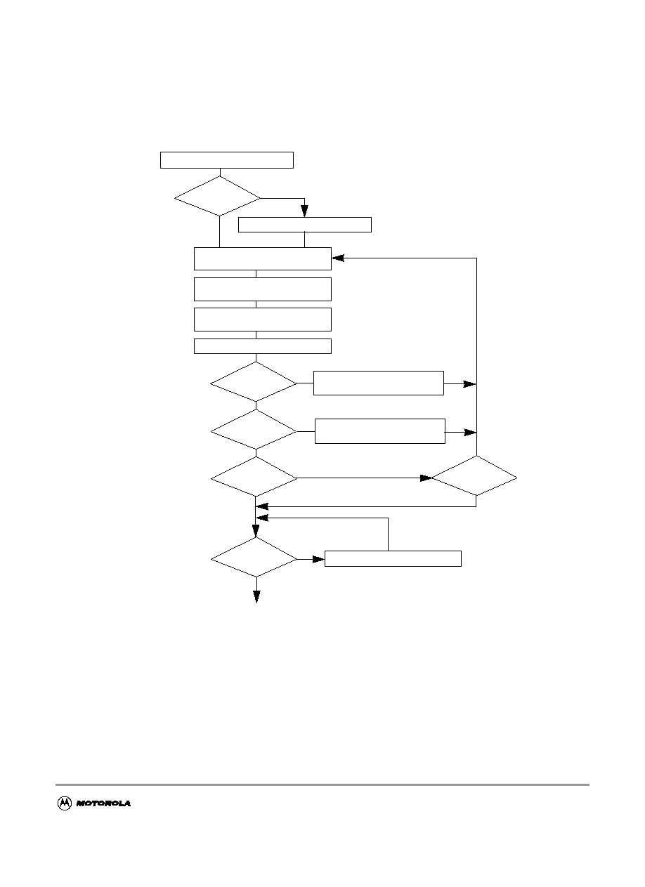
4.1.2 Program and Erase Sequences in User Mode
A Command State Machine is used to supervise the write sequencing for program and erase. The
erase-verify command follows the same flow. Before starting a command sequence, it is necessary to
verify that there is no pending access error or protection violation in either of the Flash blocks (the
ACCERR and PVIOL flags should be cleared in the FSTAT registers) It is then required to set the PPAGE
register, as well as to set the Flash configuration register FCNFG. The procedure is as follows:
1.
Verify that all ACCERR and PVIOL flags in the FSTAT register are cleared in both banks. This
requires to check the FSTAT content for both conditions of the BKSEL bit in the FCNFG register.
1.
Write to bit BKSEL in the FCNFG register to select the bank of registers corresponding to the Flash
block to be programmed or erased (see
Table 3-5
).
2.
Write to the core PPAGE register ($x030) to select one of the pages to be programmed if
programming in the $8000-$BFFF address range. There is no need to set PPAGE when
programming in the $4000-$7FFF or $C000-$FFFF address ranges.
After this possible initialization step the CBEIF flag should be tested to ensure that the address, data and
command buffers are empty. If so, the program/erase command write sequence can be started. The
following 3-step command write sequence must be strictly adhered to and no intermediate writes to the
Flash module are permitted between the 3 steps. It is possible to read any Flash register during a command
sequence. The command sequence is as follows:
1.
Write the aligned data word to be programmed to the valid Flash address space. The address and
data will be stored in internal buffers. For program, all address bits are valid. For erase, the value
of the data bytes is don't care. For mass erase, the address can be anywhere in the available address
space of the block to be erased. For sector erase the address bits[8:0] are ignored for the Flash.
2.
Write the program or erase command to the command buffer. These commands are listed in
Table
4-1
.
3.
Clear the CBEIF flag by writing a "1" to it to launch the command. When the CBEIF flag is cleared,
the CCIF flag is cleared by hardware indicating that the command was successfully launched. The
CBEIF flag will be set again indicating the address, data and command buffers are ready for a new
command sequence to begin.
The completion of the command is indicated by the CCIF flag setting. The CCIF flag only sets when all
active and pending commands have been completed.
NOTE
The Command State Machine will flag errors in program or erase write sequences by means of the
ACCERR (access error) and PVIOL (protection violation) flags in the FSTAT register. An erroneous
command write sequence will abort and set the appropriate flag. If set, the user must clear the ACCERR
or PVIOL flags before commencing another command write sequence. By writing a 0 to the CBEIF flag
the command sequence can be aborted after the word write to the Flash address space or after writing a
command to the FCMD register and before the command is launched. Writing a "0" to the CBEIF flag in
this way will set the ACCERR flag.
F
r
e
e
s
c
a
l
e
S
e
m
i
c
o
n
d
u
c
t
o
r
,
I
Freescale Semiconductor, Inc.
For More Information On This Product,
Go to: www.freescale.com
n
c
.
.
.
Block Guide -- FTS128K V01.03
35
A summary of the program algorithm is shown in
Figure 4-2
. For the erase algorithm, the user writes
either a mass or sector erase command to the FCMD register.
Figure 4-2 Example Program Algorithm
Write: Register FCLKDIV
Read: Register FCLKDIV
Bit FDIVLD set?
Write: Array Address and
Write: Register FCMD
Program Command $20
Write: Register FSTAT
yes
no
Clear bit CBEIF $80
CBEIF
Set?
Bit
yes
Clock Register
Written
Check
1.
2.
3.
Clear bit ACCERR $10
Write: Register FSTAT
no
yes
no
Protection
Violation Check
Access
Error Check
Read: Register FSTAT
CCIF
Set?
Bit
no
no
Address, Data,
Command
Buffer Empty Check
Next Write?
yes
EXIT
no
Program Data
Clear bit PVIOL $20
Write: Register FSTAT
yes
PVIOL
Set?
Bit
ACCERR
Set?
Bit
Bit Polling for
Command
Completion Check
Read: Register FSTAT
yes
NOTE: command sequence
aborted by writing $00 to
FSTAT register.
NOTE: command sequence
aborted by writing $00 to
FSTAT register.
F
r
e
e
s
c
a
l
e
S
e
m
i
c
o
n
d
u
c
t
o
r
,
I
Freescale Semiconductor, Inc.
For More Information On This Product,
Go to: www.freescale.com
n
c
.
.
.

Block Guide -- FTS128K V01.03
36
4.1.3 Valid Flash Commands
Table 4-1
summarizes the valid Flash User commands. Also shown are the effects of the commands on
the Flash
WARNING
It is not permitted to program a Flash word without first erasing the sector in which that word
resides.
4.1.4 Illegal Flash Operations
The ACCERR flag will be set during the command write sequence if any of the following illegal
operations are performed causing the command write sequence to immediately abort:
1.
Writing to the Flash address space before initializing FCLKDIV.
2.
Writing to the Flash address space in the range $8000-$BFFF when PPAGE register does not select
a 16K bytes page in the Flash block selected by the BKSEL bit in the FCNFG register.
3.
Writing to the Flash address space $4000-$7FFF or $C000-$FFFF with the BKSEL bit in the
FCNFG register not selecting Flash block 0.
4.
Writing a misaligned word or a byte to the valid Flash address space.
5.
Writing to the Flash address space while CBEIF is not set.
6.
Writing a second word to the Flash address space before executing a program or erase command on
the previously written word.
7. Writing to any Flash register other than FCMD after writing a word to the Flash address space.
Table 4-1 Valid Flash Commands
FCMD
Meaning
Flash
$05
Erase
Verify
Verify all memory bytes of the Flash block
are erased.
If the array is erased the BLANK bit will set in
the FSTAT register, upon command
completion.
$20
Program
Program a word (two bytes).
$40
Sector
Erase
Erase 256 words of Flash.
$41
Mass
Erase
Erase all the Flash array.
A mass erase of the full block is only possible
when FPLDIS, FPHDIS and FPOPEN are
set.
F
r
e
e
s
c
a
l
e
S
e
m
i
c
o
n
d
u
c
t
o
r
,
I
Freescale Semiconductor, Inc.
For More Information On This Product,
Go to: www.freescale.com
n
c
.
.
.

Block Guide -- FTS128K V01.03
37
8.
Writing a second command to the FCMD register before executing the previously written
command.
9. Writing an invalid user command to the FCMD register in user mode.
10. Writing to any Flash register other than FSTAT (to clear CBEIF) after writing to the command
register, FCMD.
11. The part enters STOP mode and a program or erase command is in progress. The command is
aborted and any pending command is killed.
12.
When security is enabled, a command other than Mass-Erase originating from a non-secure
memory or from the Background Debug Mode is written to FCMD.
13.
A "0" is written to the CBEIF bit in the FSTAT register.
The ACCERR flag will not be set if any Flash register is read during the command sequence.
If the Flash array is read during execution of an algorithm (i.e. CCIF bit in the FSTAT register is low) the
read will return non valid data and the ACCERR flag will not be set
If an ACCERR flag is set in either of the FSTAT registers the Command State Machine is locked. It is not
possible to launch another command on either block until the ACCERR flag is cleared.
The PVIOL flag will be set during the command write sequence after the word write to the Flash address
space if any of the following illegal operations are performed, causing the command sequence to
immediately abort:
1.
Writing a Flash address to program in a protected area of the Flash.
2.
Writing a Flash address to erase in a protected area of the Flash.
3.
Writing the mass erase command to FCMD while any protection is enabled. See Protection register
description in
3.3.5
.
If a PVIOL flag is set in either of the FSTAT registers the Command State Machine is locked. It is not
possible to launch another command on either block until the PVIOL flag is cleared.
4.2 Wait Mode
When the MCU enters WAIT mode and if any command is active (CCIF=0), that command and any
pending command will be completed.
The FTS256K module can recover the part from WAIT if the interrupts are enabled (see
Section 6
).
4.3 Stop Mode
If a command is active (CCIF = 0) when the MCU enters the STOP mode, the command will be aborted,
and the data being programmed or erased is lost. The high voltage circuitry to the flash will be switched
off when entering STOP mode. CCIF and ACCERR flags will be set. If commands are active in both
blocks when STOP occurs, then all the corresponding CCIF and ACCERR flags will be set. Upon exit
F
r
e
e
s
c
a
l
e
S
e
m
i
c
o
n
d
u
c
t
o
r
,
I
Freescale Semiconductor, Inc.
For More Information On This Product,
Go to: www.freescale.com
n
c
.
.
.

Block Guide -- FTS128K V01.03
38
from STOP the CBEIF flag is set and any pending command will not be executed. All ACCERR flags must
be cleared before returning to normal operation.
WARNING
As active commands are immediately aborted when the MCU enters STOP mode, it is strongly
recommended that the user does not use the STOP command during program and erase execution.
4.4 Background Debug Mode
In Background Debug Mode (BDM), the FPROT registers are writable. If the chip is unsecured then all
Flash commands listed in
Table 4-1
can be executed. In special single chip mode if the chip is secured
then the only possible command to execute is Mass Erase.
4.5 Flash Security
The Flash module provides the necessary security information to the rest of the chip. After each reset, the
Flash module determines the security state of the microcontroller as defined in section
3.3.2
.
The contents of the Flash Protection/Options byte at $FF0F in the Flash Protection/Options Field must be
changed directly by programming $FF0F when the device is unsecured and the higher address sector is
unprotected. If the Flash Protection/Options byte is left in the secure state, any reset will cause the
microcontroller to return to the secure operating mode
4.5.1 Unsecuring the Flash via the Backdoor Key Access
The microcontroller may only be unsecured by using the Backdoor Key Access feature. This requires
knowledge of the contents of the backdoor keys, four 16-bit words programmed in the Flash 0 at addresses
$FF00 - $FF07. With the KEYEN and KEYACC bits set, a write to a backdoor key address triggers a
comparison between the written data and the backdoor key data stored in the Flash. If all four words of
data are written to the correct addresses in the correct order and the data matches the backdoor keys stored
in the Flash the microcontroller will be unsecured. The data must be written to the backdoor keys
sequentially staring with $FF00-1 and ending with $FF06-7.When the KEYACC bit is set reads of the
Flash array will return invalid data.
The user code stored in the Flash must have a method of receiving the backdoor key from an external
stimulus. This external stimulus would typically be through one of the on-chip serial ports.
If the KEYEN bit is set in the FCNFG register, the flash can be unsecured by the following Back Door
Access Sequence:
1.
Set the KEYACC bit in the Flash Configuration Register FCNFG.
2.
Write the correct four 16-bit words backdoor keys to Flash addresses $FF00 - $FF07 sequentially
starting with $FF00.
3. Clear the KEYACC bit.
F
r
e
e
s
c
a
l
e
S
e
m
i
c
o
n
d
u
c
t
o
r
,
I
Freescale Semiconductor, Inc.
For More Information On This Product,
Go to: www.freescale.com
n
c
.
.
.

Block Guide -- FTS128K V01.03
39
4.
If all four 16-bit words match the Flash content, the MCU is unsecured and bits SEC[1:0] in the
FSEC register are forced to the unsecure state, `10'.
5. If any of the four 16-bit words does not match the Flash content the MCU remains secured.
After the Backdoor Access Sequence has been correctly matched, the microcontroller will be unsecured.
The Flash security byte can be programmed to the unsecure state, if desired.
In the unsecured state the user has full control of the contents of the four word Backdoor Key by
programming it in bytes $FF00 - $FF07 of the Flash Protection/Options Field.
The security of the Flash module as defined in the Flash Security/Options byte ($FF0F) is not changed by
unsecuring the flash module using the back door access scheme. The Back Door Comparison Key stored
in words $FF00 - $FF07 is unaffected by the Back Door Access sequence. After the next reset sequence,
the security state of the Flash module is determined by the Flash Security/Options byte ($FF0F)}. The
back door access method of unsecuring the microcontroller has no effect on the program and erase
protections defined in the Flash Protection Register FPROT.
It is not possible to unsecure the microcontroller in Special Single Chip mode by the Backdoor Access Key
sequence via the Background Debug Mode.
F
r
e
e
s
c
a
l
e
S
e
m
i
c
o
n
d
u
c
t
o
r
,
I
Freescale Semiconductor, Inc.
For More Information On This Product,
Go to: www.freescale.com
n
c
.
.
.

Block Guide -- FTS128K V01.03
40
F
r
e
e
s
c
a
l
e
S
e
m
i
c
o
n
d
u
c
t
o
r
,
I
Freescale Semiconductor, Inc.
For More Information On This Product,
Go to: www.freescale.com
n
c
.
.
.

Block Guide -- FTS128K V01.03
41
Section 5 Resets
5.1 General
If a reset occurs while any command is in progress that command will be immediately aborted. The state
of the word being programmed or the sector / block being erased is not guaranteed.
F
r
e
e
s
c
a
l
e
S
e
m
i
c
o
n
d
u
c
t
o
r
,
I
Freescale Semiconductor, Inc.
For More Information On This Product,
Go to: www.freescale.com
n
c
.
.
.

Block Guide -- FTS128K V01.03
42
F
r
e
e
s
c
a
l
e
S
e
m
i
c
o
n
d
u
c
t
o
r
,
I
Freescale Semiconductor, Inc.
For More Information On This Product,
Go to: www.freescale.com
n
c
.
.
.

Block Guide -- FTS128K V01.03
43
Section 6 Interrupts
6.1 General
The FTS128K module can generate an interrupt when all Flash commands are completed or the address,
data and command buffers are empty.
NOTE
Vector addresses and their relative interrupt priority are determined at the MCU level
6.2 Description of Interrupt Operation
Figure 6-1
shows the logic used for generating interrupt via the relevant block.
This system uses the CBEIF and CCIF flags in combination with the enable bits CBIE and CCIE in
addition to the BKSEL bit to discriminate for the interrupt generation. By taking account of the possible
selected bank, the system is prevented from generating false interrupts when the command buffer is empty
in an unselected bank.
Table 6-1 Flash Interrupt Sources
Interrupt Source
Interrupt Flag
Local Enable
Global (CCR)
Mask
Flash Address, Data and
Command Buffers empty
CBEIF
(FSTAT from any Flash block)
CBEIE
I Bit
All Commands are
completed on Flash
CCIF
(FSTAT from any Flash block)
CCIE
I Bit
F
r
e
e
s
c
a
l
e
S
e
m
i
c
o
n
d
u
c
t
o
r
,
I
Freescale Semiconductor, Inc.
For More Information On This Product,
Go to: www.freescale.com
n
c
.
.
.

Block Guide -- FTS128K V01.03
44
Figure 6-1 FTS128K Flash Interrupt Implementation
For a detailed description of the register bits refer to the Flash Configuration register and Flash Status
register sections (respectively
3.3.4
and
3.3.6
).
Flash 0 CBEIF
Flash Interrupt Request
Block 0 select
CBEIE
Flash 1 CBEIF
Block 1 select
Flash 0 CCIF
Block 0 select
CCIE
Flash 1 CCIF
Block 1 select
F
r
e
e
s
c
a
l
e
S
e
m
i
c
o
n
d
u
c
t
o
r
,
I
Freescale Semiconductor, Inc.
For More Information On This Product,
Go to: www.freescale.com
n
c
.
.
.

Block Guide -- FTS128K V01.03
45
Block Guide End Sheet
F
r
e
e
s
c
a
l
e
S
e
m
i
c
o
n
d
u
c
t
o
r
,
I
Freescale Semiconductor, Inc.
For More Information On This Product,
Go to: www.freescale.com
n
c
.
.
.

Block Guide -- FTS128K V01.03
46
FINAL PAGE OF
46
PAGES
F
r
e
e
s
c
a
l
e
S
e
m
i
c
o
n
d
u
c
t
o
r
,
I
Freescale Semiconductor, Inc.
For More Information On This Product,
Go to: www.freescale.com
n
c
.
.
.