 | –≠–ª–µ–∫—Ç—Ä–æ–Ω–Ω—ã–π –∫–æ–º–ø–æ–Ω–µ–Ω—Ç: D83S | –°–∫–∞—á–∞—Ç—å:  PDF PDF  ZIP ZIP |
25 Locust St, Haverhill, Massachusetts 01830 ∑ Tel: 800/252-7074, 978/374-0761 ∑ FAX: 978/521-1839
e-mail: sales@freqdev.com ∑ Web Address: http://www.freqdev.com
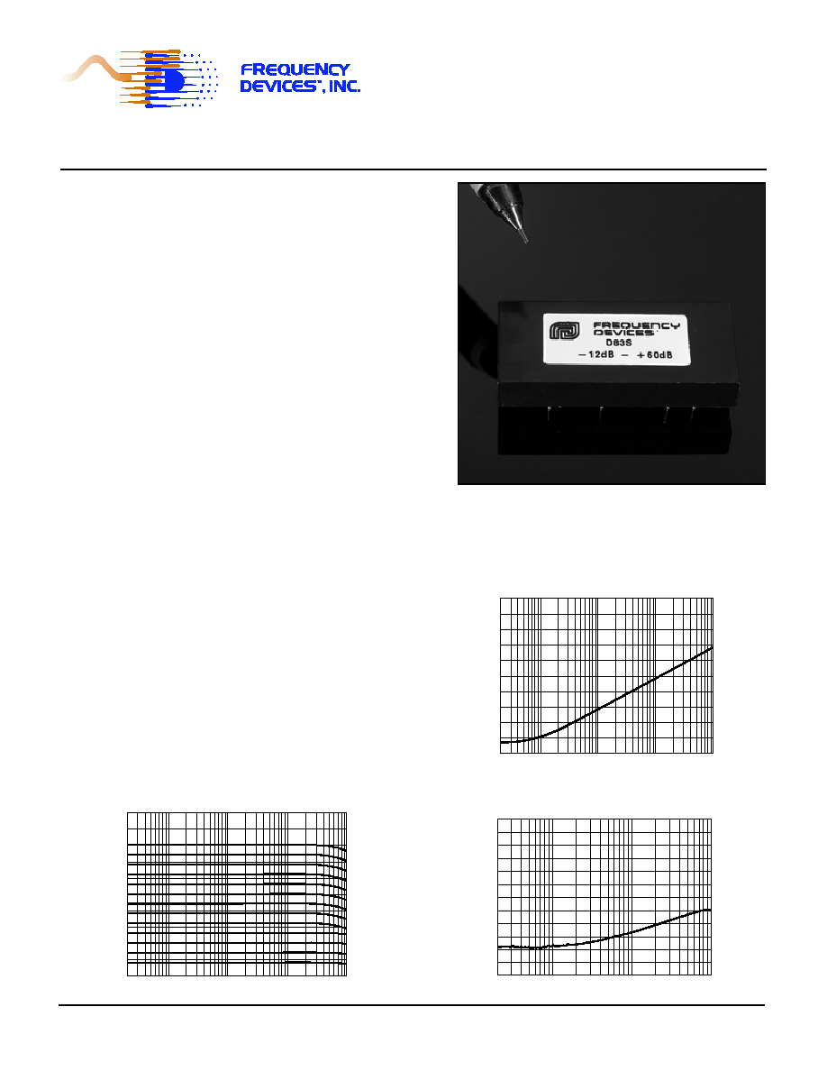
-12 dB to +60 dB
D83S Series
Programmable Amplifier
Features/Benefits:
∑ Full power bandwidth to 100 kHz for wide dynamic
range applications
∑ Compact 1.8" x 0.8" x 0.3" (32 pin DIP) size minimizes
board space requirements
∑ Serial interface and software protocol allowing
operation on a simple three wire bus.
∑ Data out line allows data verification and cascading of
multiple amplifiers over the same serial interface.
∑ Plug-in ready-to-use, reducing engineering design and
manufacturing time.
Applications
∑ Data acquisition
∑ Test equipment
∑ Remote instrumentation systems
∑ Ground loop elimination in remote measurements
∑ Improvements in system dynamic range and resolution
∑ Telemetry
∑ Process control
∑ Digitally controlled auto ranging systems
∑ Medical, Scientific & engineering research
Description
The D83S Series programmable amplifiers are digitally
controlled gain modules that were designed for condition-
ing DC-coupled wide-band signals (AC coupled-optional).
They are programmable from -12 dB to +60 dB in 6 dB
steps with an 8-bit serial data stream for gain selection
using clock, data and strobe inputs.
Other standard performance features include differential
input, single ended output, 5V interface logic, and low
noise and distortion, making this plug-in ready-to-use
amplifier ideal for many signal conditioning applications.
Available options include AC coupled input and/or differ-
ential output.
5k
100
20
-20
+30
+40
+60
Hz
50
1k
200
500
2k
10k
20k
50k 100k
+70
+80
+50
d
B
g
+20
+10
+0
-10
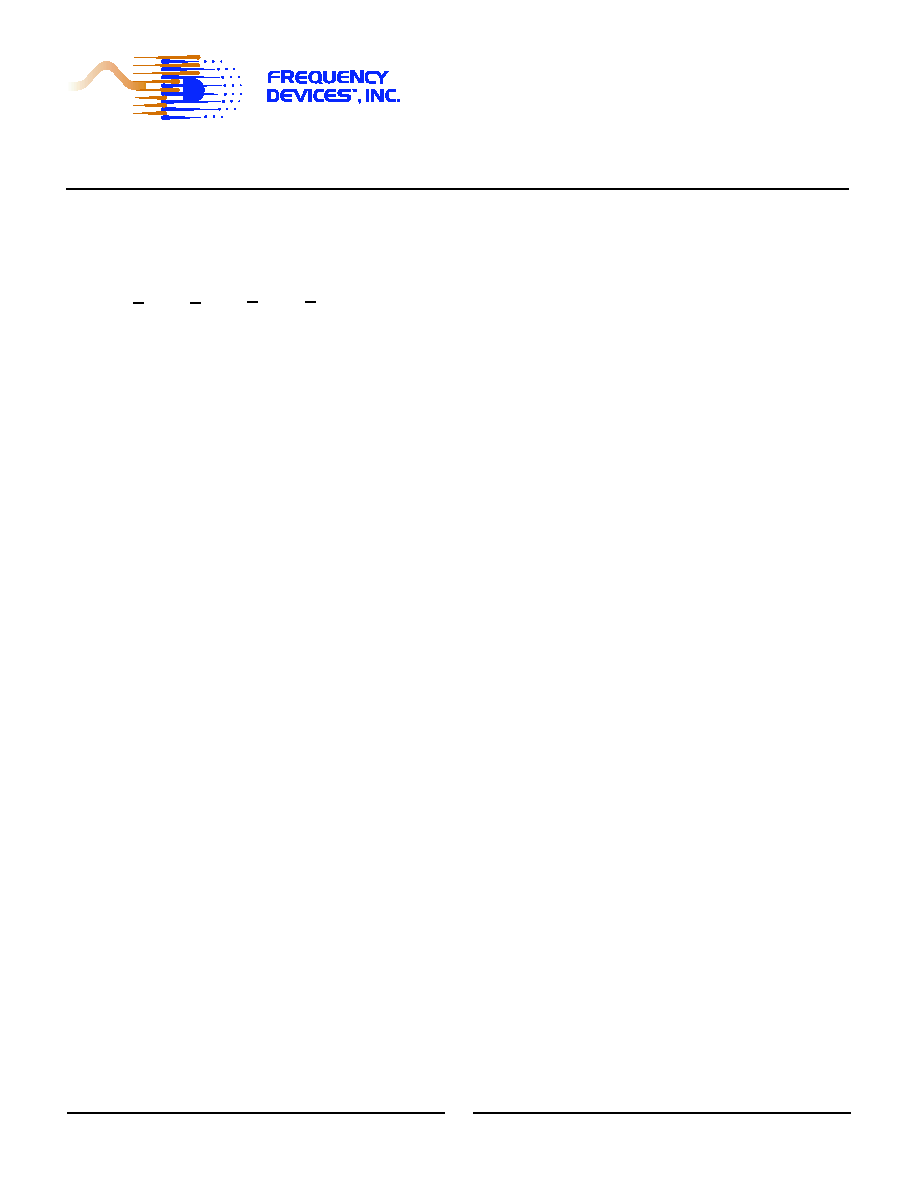
Frequency Response
Common Mode Rejection Ratio
5k
100
20
-100
-50
-40
-20
Hz
50
1k
200
500
2k
10k
20k
50k 100k
-10
+0
-30
d
B
g
-60
-70
-80
-90
Total Harmonic Distortion + Noise
5k
100
20
-120
-70
-60
-40
Hz
50
1k
200
500
2k
10k
-30
-20
-50
d
B
g
-80
-90
-100
-110
-10
+0
U.S. Selling Price (1-9)
$240.00 each
Orders for Export
U.S. Selling Price + 20%
Minimum Order Value $150.00
F.O.B. Haverhill, MA
Lead-Time: 3-4 weeks A.R.O
Accept Visa, Mcard, Amex
Gain Amplifier
D83S Series
Digital Programming & Control
25 Locust St, Haverhill, Massachusetts 01830 ∑ Tel: 800/252-7074, 978/374-0761 ∑ FAX: 978/521-1839
e-mail: sales@freqdev.com ∑ Web Address: http://www.freqdev.com
The D83S programs via a three terminal serial data interface over a gain range from 0.25 (~-12dB) to
1024 (~+60dB) using Clock (C), Strobe (S) and Data inputs (Di). A Data out (Do) connection is provided
to permit cascading of multiple D83S's or "looping" of the input data to verify the programmed setting.
Two stages of programmable gain/attenuation are used to optimize the D-C offset and gain bandwidth
performance. The gain programming equation is:
G=[1+3xD0+12xD1+48xD2+64xD3]x[1/4+(1/4)xD4+(1/2)xD5+D6]x[1+3xD7]
where D0 - D7 = "0" or "1"
Note: the use of the compliments of D0, D1, D2 and D3.
C, S and Di Input Specifications
Input Data Levels
(Cmos/TTL Logic)
Input Voltage (Vd = 5Vdc)
Low Level In
0 Vdc min.,
1.5 Vdc max.
High Level In
3.5 Vdc min.,
5.0 Vdc max.
Input Current
Low Level In
-10-5
µA typ., -1 µA max.
High Level In
+10-5
µA typ., +1 µA max.
Input Capacitance
5 pF typ.,
7.5 pF max.
Recommended Programming Table
All combinations of programming inputs produce valid gain settings as determined by the gain equation
but can result in unusual values of gain. To minimize the multiplication of D-C offset and to maximize the
bandwidth at high gains the following is the recommended programming format for binary weighted gains
from 1/4 (~-12dB) to 1024 (~60dB).
Gain ( V/V ) Gain (~dB) D0
D1
D2
D3
D4
D5
D6
D7
1/4
-12.04
1
1
1
1
0
0
0
0
1/2
-6.02
1
1
1
1
1
0
0
0
1
0.00
1
1
1
1
1
1
0
0
2
+6.02
1
1
1
1
1
1
1
0
4
+12.04
0
1
1
1
1
1
0
0
8
+18.06
0
1
1
1
1
1
1
0
16
+24.08
0
0
1
1
1
1
0
0
32
+30.10
0
0
1
1
1
1
1
0
64
+36.12
0
0
0
1
1
1
0
0
128
+42.14
0
0
0
0
1
1
0
0
256
+48.16
0
0
0
0
1
1
1
0
512
+54.19
0
0
0
0
1
1
0
1
1024
+60.21
0
0
0
0
1
1
1
1
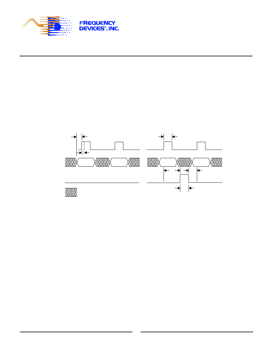
Programming Sequence The programming input circuit is a CD4094 series 8 bit shift register with
latches. It requires an 8 bit input serial data stream, Di (D0 to D7), a clock C to shift and a strobe S to
latch the data (see note 1). A timing sequence must be observed to insure accurate shifting and latching
of the input data. The input data bits, D0 through D7 are entered in reverse order, i.e. the MSB, D7, is the
first bit to be entered followed by D6 etc. and ending with the LSB, D0 (refer to timing diagram).
2
Gain Amplifier
D83S Series
Digital Programming & Control
25 Locust St, Haverhill, Massachusetts 01830 ∑ Tel: 800/252-7074, 978/374-0761 ∑ FAX: 978/521-1839
e-mail: sales@freqdev.com ∑ Web Address: http://www.freqdev.com
The Clock shifts the input data Di through the shift registers when it transitions from low to high. For the
input data to be accurately received, it must have been present for at least Ts at the time of the rising
clock transition. The maximum clock pulse frequency is 1.25MHz.
Data from the shift registers propagates through the latches when the strobe is high. Data is latched
when the Strobe transitions from high to low. To retain a programmed setting it is necessary to hold the
strobe low (or to shut off the clock). Keeping the strobe low will allow the clock to shift a new set of input
data into the registers without changing the latched setting.
To latch a new set of data the strobe must be set to its high state, after the last bit of the new input word
(D0) has been shifted in (>Tcs), held high for a minimum time of Tsw and then returned to its low state to
latch and hold the setting. The return of S to its low state must occur before the rise of the clock that
accepts the D7 of the next data word (Tsc>0).
Notes:
1.)
Data is shifted into register on positive edge of clock.
2.)
Data is latched on negative edge of strobe.
3.)
Ts is set up time (valid data before clock).
4.)
Tcs is time between D0 clock and start of strobe.
5.)
Tsw is strobe width.
6.)
Tsc is time between strobe end and D7 clock (next word).
7.)
Tcw is clock width.
8.)
Th is hold time (Valid data after clock rising edge).
Minimum Setup Times
Ts
>125nS
Time data must be present before rise of clock pulse.
Tcs
>260nS
Time from rise of Clock for last data bit, D0, to rise of Strobe pulse.
Tsw
>200nS
Strobe width.
Tsc
>0nS
Time from fall of Strobe to rise of next Clock pulse.
Tcw
>200nS
Clock pulse width.
Cf
1.25 MHz
Maximum Clock pulse frequency.
Th
>5nS
Time data must be valid after rise of clock pulse.
Caution!!
Note 1: The C, P and Di inputs are Tri-state C-MOS logic. They contain protection circuitry to guard against damage due to high static voltages or
electric fields, however the application of any voltages higher than the +5V or lower than the 0V supply voltages can cause permanent damage.
These inputs must always be connected to an appropriate logic voltage level. Permanent damage can also result if C, P and Di are allowed to float
unconnected. If the D83S is used in a configuration where these inputs can become disconnected from their drive circuits, or if their drive circuits
are not powered by the same +5V source, it is recommended to use 10k
pull up resistors to +5V on these inputs.
=Don't care
Strobe
Data
D7
Valid Input
D6
Valid Input
D0
Valid Input
D7
Valid Input
Ts
Tcw
Tcs
Tsc
Clock
Tsw
Th > 5ns
Timing Diagram
3
Specification
(25∞C and Vs ± 15 Vdc)
D83S Series
Pin-Out and Package Data
Ordering Information
25 Locust St, Haverhill, Massachusetts 01830 ∑ Tel: 800/252-7074, 978/374-0761 ∑ FAX: 978/521-1839
e-mail: sales@freqdev.com ∑ Web Address: http://www.freqdev.com
4
Ordering Information
Analog Input Characteristics
Configuration
DC coupled, differential Input
AC Coupled (Optional)
Fixed @ 10 Hz
Impedance
1 M
22pF
Bias Current
20 pA max.
Offset Current
10 pA max.
Voltage Range
±10 Vpeak
Max. Safe Voltage
±Vs
Common Mode Rejection Ratio
Typ. 80 dB @ 1 kHz
Min. 60 dB @ 1 kHz
Noise Voltage Density,
RTI
20 nV/ Hz @ 1 kHz, G=1,024
Analog Output Characteristics
Configuration
Single ended, DC coupled
Differential Output
(Optional)
Impedance
<1
typ., 10 max.
Current
(linear operation)
±5 mA max.
Offset Voltage
2 mV RTI, NTE 40 mV max.
Offset Temp. Coeff.
±(5 + 100/G) µV/∞C
General Analog Characteristics
Gain (programmable)
0.25X to 1,024X in factors of 2
Gain Tolerance
±0.10 dB
Distortion
(0 dB gain @ 3.5 Vrms)
-86 dB @ 1 kHz typ.
Full Power Bandwidth
(0 dB gain)
100 kHz
Power Supplies (±Vs), +Vd
Rated Voltage
±15 Vdc, +5 Vdc
Operating Range
±5 to ±18 Vdc, 5 ± 0.5 Vdc
Maximum Safe Voltage
±18 Vdc, +5.5 Vdc
Quiescent Current
±15 V
±12 mA
+5 V
+0.2 mA
Temperature
Operating
0 to +70∞C
Storage
-25 to +85∞C
Programmable
Instrumentation
Amplifier
Inverting
Amplifier
+OUT
-OUT
Do
+IN
-IN
C
Di
S
Programmable
Gain Stage
4094 Series 8 Bit
Shift Register
1.80
0.30
0.15 (min)
Side View
0.025 dia.
S
STROBE
ALL DIMENSIONS ARE IN INCHES
C
CLOCK
ALL CASE DIMENSIONS ± 0.01"
DI
DATA IN
GRID DIMENSIONS
DO
DATA OUT
0.10" X 0.10"
Note: NC pin is used as "-OUT" for differential output option
+Vs
-IN
GND
Bottom View
-Vs
+5V
S
Di
C
Do
+IN
+OUT
NC/-OUT
0.80
(note)
Functional Schematic
D83S-D
Options
A - AC Coupled Input
D - Differential Output
We hope the information given here will be helpful. The information is based on data and our best knowledge, and we consider the information to be true and accurate. Please read all statements,
recommendations or suggestions herein in conjunction with our conditions of sale which apply to all goods supplied by us. We assume no responsibility for the use of these statements,
recommendations or suggestions, nor do we intend them as a recommendation for any use which would infringe any patent or copyright.
PR-00D83S-01