Econo IPM series
600V / 50A 7
in one-package
7MBP50TEA060
Features
∑ Temperature protection provided by directly detecting the junction
temperature of the IGBTs
∑ Low power loss and soft switching
∑ High performance and high reliability IGBT with overheating protection
∑ Higher reliability because of a big decrease in number of parts in
built-in control circuit
Maximum ratings and characteristics
Absolute maximum ratings(at Tc=25∞C unless otherwise specified)
Symbol Rating Unit
Min. Max.
Bus voltage DC
Surge
Short operating
Collector-Emitter voltage *1
Collector current DC
1ms
Duty=76.1% *2
Collector power dissipation One transistor *3
Collector current DC
1ms
Forward current diode
Collector power dissipation One transistor *3
Supply voltage of Pre-Driver *4
Input signal voltage *5
Input signal current
Alarm signal voltage *6
Alarm signal current *7
Junction temperature
Operating case temperature
Storage temperature
Solder temperature *8
Isolating voltage (Terminal to base, 50/60Hz sine wave 1min.)
Screw torque Mounting (M5)
V
DC
V
DC(surge)
V
SC
V
CES
I
C
I
CP
-I
C
P
C
I
C
I
CP
I
F
P
C
V
CC
V
in
I
in
V
ALM
I
ALM
T
j
T
opr
T
stg
T
sol
V
iso
Item
0
0
200
0
-
-
-
-
-
-
-
-
-0.5
-0.5
-
-0.5
-
-
-20
-40
-
-
-
450
500
400
600
50
100
50
144
30
60
30
144
20
Vcc+0.5
3
Vcc
20
150
100
125
260
AC2500
3.5
V
V
V
V
A
A
A
W
A
A
A
W
V
V
mA
V
mA
∞C
∞C
∞C
∞C
V
N∑m
Inverter
Note
*1 : Vces shall be applied to the input voltage between terminal P and U or ,u or W, N and U or V or W
*2 : 125
∞C
/FWD Rth(j-c)/(Ic x VF MAX)=125/1.263/(50 x 2.6) x 100=76.1%
*3 : Pc=125
∞C
/IGBT Rth(j-c)=125/0.87=144W [Inverter]
Pc=125
∞C
/IGBT Rth(j-c)=125/0.87=144W [Breake]
*4 : VCC shall be applied to the input voltage between terminal No.4 and 1, 8 and 5, 12 and 9, 14 and 13
*5 : Vin shall be applied to the input voltage between terminal No.3 and 1, 7 and 5, 11 and 9, 16,17,18 and 13.
*6 :VALM shall be applied to the voltage between terminal No.2 and 1, No6 and 5, No10 and 9, No.19 and 13.
*7 : IALMshall be applied to the input current to terminal No.2,6,10 and 19.
*8 : Immersion time 10
±
1sec.

7MBP50TEA060
IGBT-IPM
Control circuit
Item Symbol Condition Min. Typ. Max. Unit
Supply current of P-line side pre-driver(one unit)
Supply current of N-line side pre-driver
Input signal threshold voltage (on/off)
Input zener voltage
Alarm signal hold time
Current limit resistor
Switching Trequency : 0 to 15kHz
Tc=-20 to 125∞C Fig.7
ON
OFF
Rin=20k ohm
Tc=-20∞C Fig.2
Tc=25∞C Fig.2
Tc=125∞C Fig.2
Alarm terminal
I
ccp
I
CCN
V
in(th)
V
Z
t
ALM
R
ALM
-
-
1.00
1.25
-
1.1
-
-
1425
-
-
1.35
1.60
8.0
-
2.0
-
1500
18
65
1.70
1.95
-
-
-
4.0
1575
mA
mA
V
V
V
ms
ms
ms
ohm
Protection Section ( Vcc=15V)
Turn-on time
Turn-off time
Reverse recovery time
Maximum Avalanche Energy
(A non-repetition)
ton VDC=300V,Tj=125∞C
toff IC=50A Fig.1, Fig.6
trr VDC=300V, IC=50A Fig.1, Fig.6
P
AV
Internal wiring inductance=50nH
Main circuit wiring inductace=54nH
Thermal characteristics( Tc=25∞C)
Item Symbol Min. Typ. Max. Unit
Junction to Case thermal resistance *9
Case to fin thermal resistance with compound
Rth(j-c)
Rth(j-c)
Rth(j-c)
Rth(c-f)
-
-
0.87
-
-
1.263
-
-
0.87
-
0.05 -
∞C/W
∞C/W
∞C/W
∞C/W
Inverter IGBT
FWD
Brake IGBT
Item Symbol Min. Typ. Max. Unit
DC Bus Voltage
Operating Supply Voltage of Pre-Driver
Screw torque (M5)
V
DC
V
CC
-
Recommendable value
Over Current Protection Level of Inverter circuit
Over Current Protection Level of Brake circuit
Over Current Protection Delay time
SC Protection Delay time
IGBT Chip Over Heating
Over Heating Protection Hysteresis
Under Voltage Protection Level
Under Voltage Protection Hysteresis
Electrical characteristics (at Tc=Tj=25∞C, Vcc=15V unless otherwise specified.)
Main circuit
Item Symbol Condition Min. Typ. Max. Unit
Collector current at off signal input
Collector-Emitter saturation voltage
Forward voltage of FWD
Collector current at off signal input
Collector-Emitter saturation voltage
Forward voltage of Diode
I
CES
V
CE(sat)
V
F
I
CES
V
CE(sat)
V
F
V
CE
=600V Vin terminal open.
Ic=50A
-Ic=50A
Terminal
Chip
Terminal
Chip
I
OC
I
OC
t
DOC
t
SC
T
jOH
T
jH
V
UV
V
H
Tj=125∞C
Tj=125∞C
Tj=125∞C
Tj=125∞C Fig.4
Surface of IGBT chips
75
-
45
-
-
5
-
-
-
8
150
- -
-
20
-
11.0
-
12.5
0.2
0.5
-
A
A
µs
µs
∞C
∞C
V
V
Noise Immunity ( VDC=300V, Vcc=15V, Test Circuit Fig.5)
Common mode rectangular noise
Common mode lightning surge
Pulse width 1µs, polarity ±,10minuets
Judge : no over-current, no miss operating
Rise time 1.2µs, Fall time 50µs
Interval 20s, 10 times
Judge : no over-current, no miss operating
±2.0
-
-
±5.0
-
-
Item Symbol Condition Min. Typ. Max. Unit
Item Condition Min. Typ. Max. Unit
kV
kV
-
-
400 V
13.5
15.0
16.5 V
2.5
-
3.0 Nm
Item Symbol Min. Typ. Max. Unit
Weight
Weight Wt - 270 - g
Inverter
-
-
1.0
mA
-
-
2.5
V
-
2.0
-
-
-
2.6
V
-
1.6
-
-
-
1.0
mA
-
-
2.2
V
-
1.75
-
-
-
3.3
V
-
1.9
-
1.2
-
-
µs
-
-
3.6
-
-
0.3
30
-
-
mJ
*9 For 1device, Case is under the device
Brake
Terminal
Chip
Terminal
Chip
V
CE
=600V Vin terminal open.
Ic=30A
-Ic=30A
7MBP50TEA060
IGBT-IPM
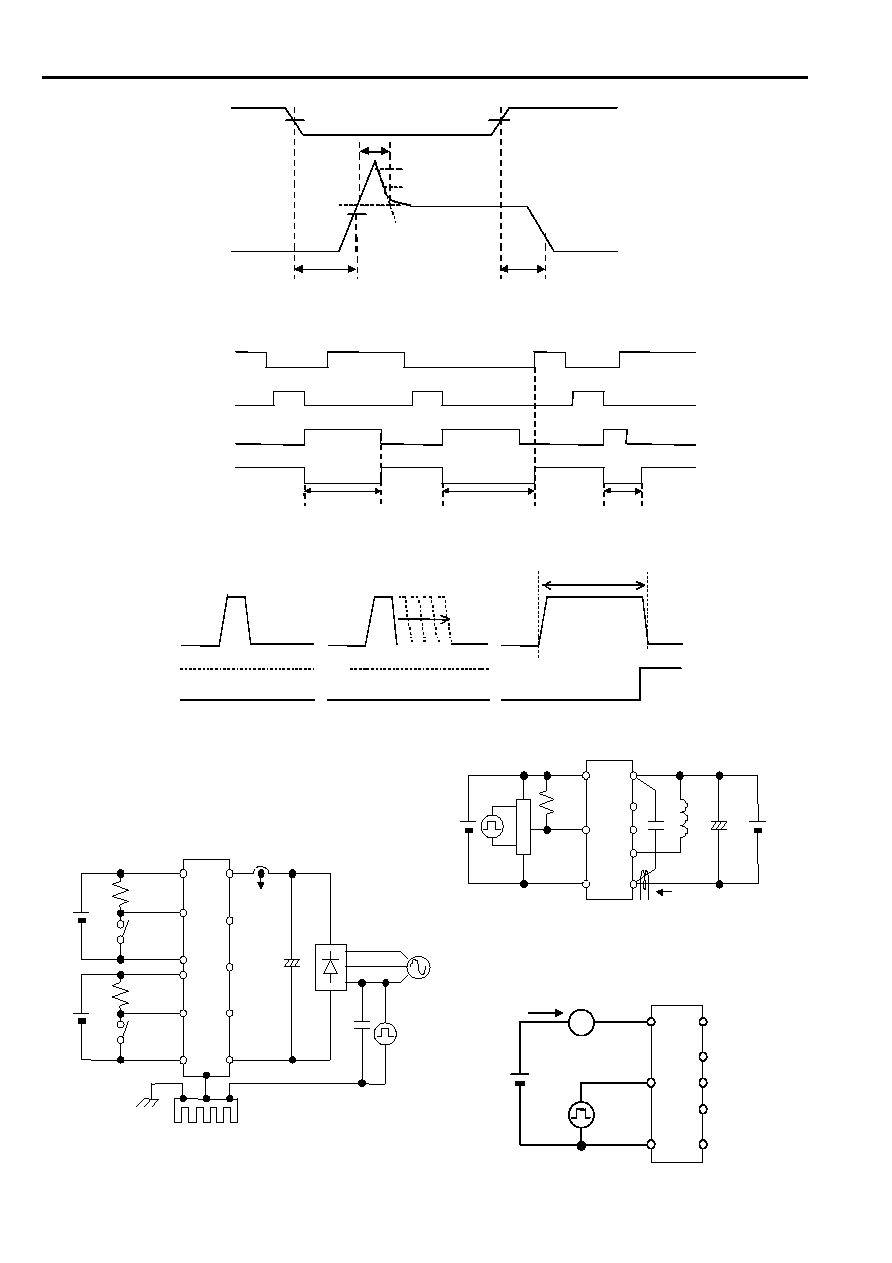
Figure 1. Switching Time Waveform Definitions
Figure 2. Input/Output Timing Diagram
Figure.4 Definition of tsc
Figure 5. Noise Test Circuit
Figure 7. Icc Test Circuit
Figure 6. Switching Characteristics Test Circuit
Ic
Ic
I
ALM
tsc
I
ALM
I
ALM
Ic
Ic
Ic
I
ALM
tsc
I
ALM
I
ALM
Ic
/Vin
Vge (Inside IPM )
Fault (Inside IPM
)
/ALM
Gate Off
on
Gate On
2ms(typ.)
off
normal
t
ALM
Max.
t
ALM >
Max.
off
Fault : Over-current,Over-heat or Under-voltage
on
alarm
t
ALM >
1
2
3
/Vin
Vge (Inside IPM )
Fault (Inside IPM
)
/ALM
Gate Off
on
Gate On
2ms(typ.)
off
normal
t
ALM
Max.
t
ALM >
Max.
off
Fault : Over-current,Over-heat or Under-voltage
on
alarm
t
ALM >
1
2
3
On
ton
Vin
Ic
Vin(th)
Vin(th)
50%
toff
10%
trr
90%
90%
On
ton
Vin
Ic
Vin(th)
Vin(th)
50%
toff
10%
trr
90%
90%
Vin
DC
15V
DC
300V
N
+
L
IPM
Ic
P
HCPL
-
4504
Vcc
GND
N
+
IPM
P
-
20 k
Vin
DC
15V
DC
300V
N
+
L
IPM
Ic
P
HCPL
-
4504
Vcc
GND
N
+
IPM
P
-
20 k
A
Vcc
Vin
GND
Icc
P
U
V
W
N
P.G
+8V
fsw
IPM
DC
15V
A
Vcc
Vin
GND
Icc
P
U
V
W
N
P.G
+8V
fsw
IPM
DC
15V
VccU
DC
15V
+
IPM
P
U
V
W
N
20k
VinU
GNDU
SW1
Vcc
DC
15V
20k
VinX
GND
SW2
Cooling
Fin
Earth
AC200V
4700p
Noise
CT
VccU
DC
15V
+
IPM
P
U
V
W
N
20k
VinU
GNDU
SW1
Vcc
DC
15V
20k
VinX
GND
SW2
Cooling
Fin
Earth
AC200V
4700p
Noise
CT
7MBP50TEA060
IGBT-IPM
Block diagram
Outline drawings, mm
Mass : 270g
U
V
W
Vcc
VinX
GND
VinY
VinZ
ALM
B
N
VinDB
VccW
ALMW
GNDW
VccV
ALMV
GNDV
P
VccU
ALMU
GNDU
VinU
VinV
VinW
Pre- Driver
Pre- Driver
Pre- Driver
Pre- Driver
Pre- Driver
Pre- Driver
Pre- Driver
Vz
R
ALM
1.5k
R
ALM
1.5k
Vz
R
ALM
1.5k
Vz
Vz
Vz
Vz
Vz
R
ALM
1.5k
Pre- Driver
Pre- Driver
Pre- Driver
Pre- Driver
Pre- Driver
Pre- Driver
Pre- Driver
Pre- Driver
Pre- Driver
Pre- Driver
Pre- Driver
Pre- Driver
Pre- Driver
Pre- Driver
4
3
2
1
8
6
5
7
12
11
10
9
14
16
13
17
18
15
19
U
V
W
Vcc
VinX
GND
VinY
VinZ
ALM
B
N
VinDB
VccW
ALMW
GNDW
VccV
ALMV
GNDV
P
VccU
ALMU
GNDU
VinU
VinV
VinW
Pre- Driver
Pre- Driver
Pre- Driver
Pre- Driver
Pre- Driver
Pre- Driver
Pre- Driver
Vz
R
ALM
1.5k
R
ALM
1.5k
Vz
R
ALM
1.5k
Vz
Vz
Vz
Vz
Vz
R
ALM
1.5k
Pre- Driver
Pre- Driver
Pre- Driver
Pre- Driver
Pre- Driver
Pre- Driver
Pre- Driver
Pre- Driver
Pre- Driver
Pre- Driver
Pre- Driver
Pre- Driver
Pre- Driver
Pre- Driver
4
4
3
2
1
8
6
5
7
12
11
10
9
14
16
13
17
18
15
19
Pre-drivers include following functions
1.Amplifier for driver
2.Short circuit protection
3.Under voltage lockout circuit
4.Over current protection
5.IGBT chip over heating protection
Package type : P622
Dimensions in mm

IGBT-IPM
Characteristics
Control circuit characteristics (Respresentative)
7MBP50TEA060
0
10
20
30
40
50
60
0
5
10
15
20
25
P ower sup ply current vs. Switching frequency
Tc=1 25∞C
N-side
P-side
P
o
w
e
r
s
u
p
p
l
y
c
u
rr
e
n
t
:
I
c
c
(
m
A
)
Switching frequency : fsw (kHz)
Vcc=13V
Vcc= 13V
Vcc=15V
Vcc= 15V
Vcc=17V
Vcc= 17V
0
0.5
1
1.5
2
2.5
12
13
14
15
16
17
18
Input signal threshold voltage
vs. P ower sup ply voltag e
In
p
u
t s
i
g
n
a
l
t
h
r
e
s
h
o
l
d
v
o
l
t
ag
e
: V
i
n
(
on
)
,
V
i
n
(
o
f
f)
(
V
)
Power supply voltag e : Vcc (V)
Tj=25∞C
Tj= 125∞C
} Vin(on)
} Vin(off)
0
2
4
6
8
10
12
14
20
40
60
80
100
120
140
Under voltage vs. Junction temp erature
Un
d
e
r
v
o
l
t
a
g
e
:
V
U
V
T
(
V
)
Ju nction temperatu re : Tj (∞C)
0
0.2
0.4
0.6
0.8
1
20
40
60
80
100
120
140
Under voltage hysterisis vs. Jnction temperature
U
nder
v
o
l
t
ag
e h
y
s
t
e
r
i
s
i
s
:
V
H
(
V
)
Ju nction temperatu re : Tj (∞C)
0
0.5
1
1.5
2
2.5
3
12
13
14
15
16
17
18
Alarm hold tim e vs. P ower sup ply voltag e
Al
a
r
m
h
o
l
d
t
i
m
e
:
t
A
L
M
(
m
Se
c
)
Power supply voltage : Vcc (V)
Tc= 100∞ C
Tc=25∞C
0
50
100
150
200
12
13
14
15
16
17
18
Over heatin g characteristics
TjOH,TjH vs. Vcc
O
v
er
h
e
ati
n
g
p
r
ot
e
c
t
i
on
: T
j
O
H
(
∞
C
)
OH
h
y
s
t
e
r
i
s
i
s
:
T
j
H
(
∞
C
)
Power supply voltag e : Vcc (V)
TjO H
TjH
7MBP50TEA060
IGBT-IPM
Main circuit characteristics (Respresentative)
0
10
20
30
40
50
60
0
0.5
1
1.5
2
2.5
3
Collector curren t vs. Collector-Em itter voltag e
Tj=25
∞ C
(Chip)
Vcc=13V
Vcc=15V
Vc c= 17V
Co
l
l
e
c
t
o
r
Cu
r
r
e
n
t
:
I
c
(
A
)
Collector-Emitter voltage : Vce (V)
0
10
20
30
40
50
60
0
0.5
1
1.5
2
2.5
3
Collector current vs. Collector-Em itter voltage
Tj=25∞C(Term inal)
Vcc=13V
Vcc= 15V
Vcc=17V
C
o
l
l
e
c
t
o
r
C
u
rr
e
n
t
:
I
c
(
A
)
Collector-Emitter voltage : Vce (V)
0
10
20
30
40
50
60
0
0.5
1
1.5
2
2.5
3
Collector curren t vs. Collector-Em itter voltag e
Tj=125∞C(Chip)
Vcc=13V
Vcc=15V
Vcc=17V
C
o
l
l
e
c
t
o
r
C
u
rre
n
t
:
I
c
(A
)
Collector-Emitter voltage : Vce (V)
0
10
20
30
40
50
60
0
0.5
1
1.5
2
2.5
3
Collector curren t vs. Collector-Em itter voltag e
Tj=125∞C(Term inal)
Vcc= 13V
Vcc=15V
Vcc=17V
C
o
l
l
e
c
t
o
r
C
u
rre
n
t
:
I
c
(A
)
Collector-Emitter voltage : Vce (V)
0
20
40
60
80
100
0
0.5
1
1.5
2
2.5
Forward current vs. Forward voltage
(Chip)
125∞ C
25∞C
F
o
r
w
ar
d
C
u
r
r
en
t
:
If
(
A
)
Forw ard voltage : Vf (V)
0
20
40
60
80
100
0
0.5
1
1.5
2
2.5
Forward current vs. Forward voltage
(Terminal)
125∞ C
25∞C
F
o
r
w
ar
d
C
u
r
r
ent
:
If
(
A
)
Forw ard voltage : Vf (V)

7MBP50TEA060
IGBT-IPM
0
1
2
3
4
5
6
0
10
20
30
40
50
60
Switching Loss vs.Collector Current
Edc=30 0V,Vcc=15 V,Tj=25∞C
Eon
Eoff
E rr
S
w
it
ch
i
n
g
l
o
s
s
:
E
o
n
,
E
o
f
f
,
E
r
r
(
m
J
/
cy
cl
e
)
Collector current : Ic (A)
0
1
2
3
4
5
6
0
10
20
30
40
50
60
Switching Loss vs.Collector Current
Edc=300V,V cc=15V,Tj=1 25∞C
Eon
Eoff
E rr
Sw
i
t
c
h
i
n
g
l
o
s
s
:
Eo
n,
Eo
f
f
,
E
r
r
(
m
J
/
c
y
c
l
e
)
Collector current : Ic (A)
0
50
100
150
0
100
200
300
400
500
600
700
Reversed b iased safe operating area
Vcc=15V,Tj
12 5
∞C
C
o
l
l
e
c
t
o
r
c
u
r
r
en
t :
Ic
(
A
)
Collector-Emitter voltag e : Vce (V)
RBS O A(Rep etitive pu lse)
0.01
0.1
1
0.001
0.01
0.1
1
Transient therm al resistance
T
h
e
r
ma
l
r
e
si
st
a
n
ce
:
R
t
h
(
j
-
c
)
(
∞
C
/
W
)
Pu lse width :Pw (sec)
FW D
IGBT
0
50
100
150
0
20
40
60
80
100 120 140 160
Power derating for IG BT
(per device)
Co
l
l
e
c
t
e
r
P
o
we
r
D
i
s
s
i
p
a
t
i
o
n
:
P
c
(
W
)
Case Temp erature : Tc (∞C)
0
50
100
150
0
20
40
60
80
100 120 140 160
Power derating for FW D
(per device)
C
o
l
l
ec
t
e
r
P
o
w
e
r
D
i
s
s
i
pat
i
o
n
:
P
c
(
W
)
Case Temp erature : Tc (∞C)

7MBP50TEA060
IGBT-IPM
10
100
1000
10000
20
30
40
50
60
70
80
Switching tim e vs. Collector current
E dc=300V,Vcc=15V,Tj=25
∞C
S
w
i
t
c
h
i
n
g
t
i
m
e
: ton
,
t
o
ff,tf (
n
S
e
c
)
Collector cu rrent : Ic (A)
toff
ton
tf
10
100
1000
10000
20
30
40
50
60
70
80
Switching tim e vs. Collector current
Ed c=300V,Vcc=15V,Tj=12 5
∞ C
S
w
i
t
c
h
i
n
g
t
i
m
e
: ton
,
t
o
ff,tf
(
n
S
e
c
)
Collector cu rrent : Ic (A)
toff
ton
tf
1
10
100
20
30
40
50
60
70
80
Reverse recovery characteristics
trr,Irr vs.IF
R
e
v
e
r
s
e
re
c
o
v
e
ry
c
u
r
r
e
n
t
:
I
r
r
(
A
)
R
e
v
e
rse
r
e
c
o
v
e
ry
t
i
m
e
:
t
rr(n
s
e
c
)
Forw ard cu rren t:IF(A)
trr125∞C
trr25∞ C
Irr125∞C
Irr25∞ C

7MBP50TEA060
IGBT-IPM
Characteristics
Dynamic Brake Characteristics (Respresentative)
0
10
20
30
40
50
60
0
0.5
1
1.5
2
2.5
3
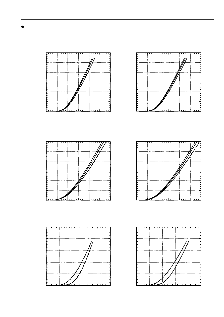
Collector current vs. Collector-Em itter voltage
Tj=25∞C
Vc c= 13V
Vc c= 15V
Vc c= 17V
C
o
l
l
e
c
t
o
r
C
u
rr
e
n
t
:
I
c
(
A
)
Collector-Emitter voltage : Vce (V)
0
10
20
30
40
50
60
0
0.5
1
1.5
2
2.5
3
Collector curren t vs. Collector-Em itter voltage
Tj=1 25∞C
Vc c= 13V
Vcc=15V
Vcc= 17V
Co
l
l
e
c
t
o
r
Cu
r
r
e
n
t
:
I
c
(
A
)
Collector-Emitter voltage : Vce (V)
0.01
0.1
1
0.001
0.01
0.1
1
Transient therm al resistance
T
h
er
m
a
l
r
e
s
i
s
t
an
c
e
:
R
t
h
(
j
-
c
)
(
∞
C
/
W
)
Pu lse width :Pw (sec)
IGB T
0
20
40
60
80
100
0
100
200
300
400
500
600
700
Reversed b iased safe operating area
Vcc=15V,Tj
1 25∞C
C
o
l
l
e
c
t
o
r
c
u
r
r
en
t :
Ic
(
A
)
Collector-Emitter voltage : Vce (V)
RBS O A(Rep etitive pu lse)
0
50
100
150
0
20
40
60
80
100 120 140 160
Power derating for IG BT
(per device)
C
o
l
l
ec
t
e
r
P
o
w
e
r
D
i
s
s
i
pat
i
o
n
:
P
c
(
W
)
Case Temp erature : Tc (∞C)