H04-004-07
Fuji Electric Co.,Ltd.
Matsumoto Factory
SPECIFICATION
Device Name :
Type Name :
Spec. No. :
IGBT - IPM
7MBP75RTB060
MS6M 0653
1
23
MS6M 0653
Sep. 17 '02
K.Sekigawa
K.Yamada
T.Fujihira
Nishiura
Sep.-17 -'02
a
Sep. 17 '02

H04-004-06
R e v i s e d R e c o r d s
Date
Classi-
fication
Ind.
Content
Applied
date
Drawn
Checked
Approved
enactment
Issued
date
MS6M 0653
2
22
K.Yamada
Sep.-17-'02
T.Fujihira
K.Sekigawa
Nishiura
a
K.Yamada
Apr.-09-'03
T.Fujihira
N.Matsuda
T.Miyasaka
Revision
a
Reliability Test Items.
Apr.-09-'03

H04-004-03
23
MS6M 0653
a
3
7MBP75RTB060
1. Outline Drawing ( Unit : mm )
P
N
W
V
U
B
1 0 9
1 0 9
1 0 9
1 0 9
9 5
9 5
9 5
9 5
6 7 . 4
6 7 . 4
6 7 . 4
6 7 . 4
1 5 . 2 4
1 5 . 2 4
1 5 . 2 4
1 5 . 2 4
5 . 0 8
5 . 0 8
5 . 0 8
5 . 0 8
5 . 0 8
5 . 0 8
5 . 0 8
5 . 0 8
1 0 . 1 6
1 0 . 1 6
1 0 . 1 6
1 0 . 1 6
1 0 . 1 6
1 0 . 1 6
1 0 . 1 6
1 0 . 1 6
1 0 . 1 6
1 0 . 1 6
1 0 . 1 6
1 0 . 1 6
1 3 . 8
1 3 . 8
1 3 . 8
1 3 . 8
5 . 5
5 . 5
5 . 5
5 . 5
5 . 0 8
5 . 0 8
5 . 0 8
5 . 0 8
2 . 5 4
2 . 5 4
2 . 5 4
2 . 5 4
3 . 2 2
3 . 2 2
3 . 2 2
3 . 2 2
88
88
88
88
74
74
74
74
20
20
20
20
20
20
20
20
17
17
17
17
10
10
10
10
2
2
2
2
0.5
0.5
0.5
0.5
2 4
2 4
2 4
2 4
2 6
2 6
2 6
2 6
2 6
2 6
2 6
2 6
0 . 5
0 . 5
0 . 5
0 . 5
�0.3
�0.3
�0.3
�0.3
�0.15
�0.15
�0.15
�0.15
�0.15
�0.15
�0.15
�0.15
�0.15
�0.15
�0.15
�0.15
�0.3
�0.3
�0.3
�0.3
�1
�1
�1
�1
�0.3
�0.3
�0.3
�0.3
�
0.3
�
0.3
�
0.3
�
0.3
�
0.3
�
0.3
�
0.3
�
0.3
�
1
�
1
�
1
�
1
4-
4-
4-
4-
�0.2
�0.2
�0.2
�0.2
�0.2
�0.2
�0.2
�0.2
�0.2
�0.2
�0.2
�0.2
�0.25
�0.25
�0.25
�0.25
�0.1
�0.1
�0.1
�0.1
8
8
8
8
31
31
31
31
22
22
22
22
17
17
17
17
9
9
9
9
7
7
7
7
22
22
22
22
0 . 6 4
0 . 6 4
0 . 6 4
0 . 6 4
2 . 5
2 . 5
2 . 5
2 . 5
-0.3
-0.3
-0.3
-0.3
-0.2
-0.2
-0.2
-0.2
16-
16-
16-
16-
2-
2-
2-
2-
+1.0
+1.0
+1.0
+1.0
+1.0
+1.0
+1.0
+1.0
-0.3
-0.3
-0.3
-0.3
+1.0
+1.0
+1.0
+1.0
14.5
14.5
14.5
14.5
6-M5
2 . 5 4
2 . 5 4
2 . 5 4
2 . 5 4
2 . 5 4
2 . 5 4
2 . 5 4
2 . 5 4
3 . 2 2
3 . 2 2
3 . 2 2
3 . 2 2
2
2
2
2
2
2
2
2
2
2
2
2
4.
5
4.
5
4.
5
4.
5
�0.1
�0.1
�0.1
�0.1
0.
1ma
x
0.
1ma
x
0.
1ma
x
0.
1ma
x
�0.3
�0.3
�0.3
�0.3
�0.1
�0.1
�0.1
�0.1
2. 5
2 . 5
2 . 5
2 . 5
10
10
10
10
8
8
8
8
1
1
1
1
�
0.3
�
0.3
�
0.3
�
0.3
Details of control terminals
0 . 6 4
( 1 1 . 5 )
(1
2)
Indication of Lot No.
Odered No. in monthly
Manufactured month
Last digit of manufactured year
(Jan.Sep.:19,Oct.:O,Nov.:N,Dec.:D)
Lot No.
Dimensions in mm
Package type : P610
1
1
1
1
4
4
4
4
7
7
7
7
1 0
1 0
1 0
1 0
1 6
1 6
1 6
1 6
a

H04-004-03
23
MS6M 0653
a
4
2Pin Descriptions
Main circuit
Description
Positive input supply voltage.
Output (U).
Output (V).
Output (W).
Negative input supply voltage.
Collector terminal of Brake IGBT.
Control circuit
Symbol
Description
GNDU High side ground (U).
VinU
Logic input for IGBT gate drive (U).
VccU
High side supply voltage (U).
GNDV High side ground (V).
VinV
Logic input for IGBT gate drive (V).
VccV
High side supply voltage (V).
GNDW High side ground (W).
VinW
Logic input for IGBT gate drive (W).
VccW
High side supply voltage (W).
GND
Low side ground.
Vcc
Low side supply voltage.
VinDB Logic input for Brake IGBT gate drive.
VinX
Logic input for IGBT gate drive (X).
VinY
Logic input for IGBT gate drive (Y).
VinZ
Logic input for IGBT gate drive (Z).
ALM
Low side alarm signal output.
B
W
N
Symbol
P
U
V

H04-004-03
23
MS6M 0653
a
5
3. Block Diagram
Pre- Driver
Pre- Driver
Pre- Driver
Pre- Driver
Pre- Driver
Pre- Driver
Pre- Driver
Over heat ing protect ion
circuit
3
R
ALM
U
V
W
N
B
P
VccU
VccV
VinU
GNDU
VccW
VinW
GNDW
VinV
GNDV
Vcc
VinX
GND
VinY
VinZ
VinDB
ALM
V
Z
V
Z
V
Z
V
Z
V
Z
1. 5k
V
Z
V
Z
2
1
6
5
4
9
8
7
11
13
10
14
15
12
16
Pre- Driver
Pre- Driver
Pre- Driver
Pre- Driver
Pre- Driver
Pre- Driver
Pre- Driver
Pre- Driver
Pre- Driver
Pre- Driver
Pre- Driver
Pre- Driver
Pre- Driver
Over heat ing protect ion
circuit
3
R
ALM
U
V
W
N
B
P
VccU
VccV
VinU
GNDU
VccW
VinW
GNDW
VinV
GNDV
Vcc
VinX
GND
VinY
VinZ
VinDB
ALM
V
Z
V
Z
V
Z
V
Z
V
Z
1. 5k
V
Z
cV
VinU
GNDU
VccW
VinW
GNDW
VinV
GNDV
Vcc
VinX
GND
VinY
VinZ
VinDB
ALM
V
Z
V
Z
V
Z
V
Z
V
Z
1. 5k
V
Z
V
Z
2
1
6
5
4
9
8
7
11
13
10
14
15
12
16
Pre-drivers include following functions
1 Amplifier for driver
2 Short circuit protection
3 Under voltage lockout circuit
4 Over current protection
5 IGBT chip over heating protection

H04-004-03
23
MS6M 0653
a
6
4Absolute Maximum Ratings
Tc25 unless otherwise specified.
Symbol
Min.
Max.
Units
Bus Voltage
DC
V
DC
0
450
V
(between terminal P and N)
Surge
V
DC(surge)
0
500
V
Shortoperating
Vsc
200
400
V
Collector-Emitter Voltage *1
Vces
0
600
V
DC
Ic
-
75
A
Collector Current
1ms
Icp
-
150
A
Duty=75.0 % *2
-Ic
-
75
A
Collector Power Dissipation
One transistor *3
Pc
-
198
W
Collector Current
DC
Ic
-
50
A
1ms
Icp
-
100
A
Forward Current of Diode
IF
-
50
A
Collector Power Dissipation
One transistor *3
Pc
-
198
W
Supply Voltage of Pre-Driver *4
Vcc
-0.5
20
V
Input Signal Voltage *5
Vin
-0.5
Vcc+0.5
V
Input Signal Current
Iin
-
3
mA
Alarm Signal Voltage *6
VALM
-0.5
Vcc
V
Alarm Signal Current *7
ALM
-
20
mA
Junction Temperature
Tj
-
150
Operating Case Temperature
Topr
-20
100
Storage Temperature
Tstg
-40
125
Isolating Voltage
(Terminal to base, 50/60Hz sine wave 1min.) *8
Screw Torque
Terminal(M5)
Mounting(M5)
Note
*1 Vces shall be applied to the input voltage between terminal P and U or or W or DB, N and U
or V or W or DB
*2 125/FWD Rth(j-c)/(Ic�VF MAX)=125/0.855/(75�2.6)�100=75.0%
*3 Pc=125/IGBT Rth(j-c)=125/0.63=198W [Inverter]
Pc=125/IGBT Rth(j-c)=125/0.63=198W [Break]
*4 VCC shall be applied to the input voltage between terminal No.3 and 1,6 and 4, 9 and 7,
11 and 10.
*5 V shall be applied to the input voltage between terminal No.2 and 1, 5 and 4, 8 and 7,
13,14,15 and 10.
*6 shall be applied to the voltage between terminal No.16 and 10.
*7 shall be applied to the input current to terminal No.16.
*8 50Hz/60Hz sine wave 1 minute.
-
V
Nm
3.5
-
Items
Viso
-
AC2500
Inverter
Brake

H04-004-03
23
MS6M 0653
a
7
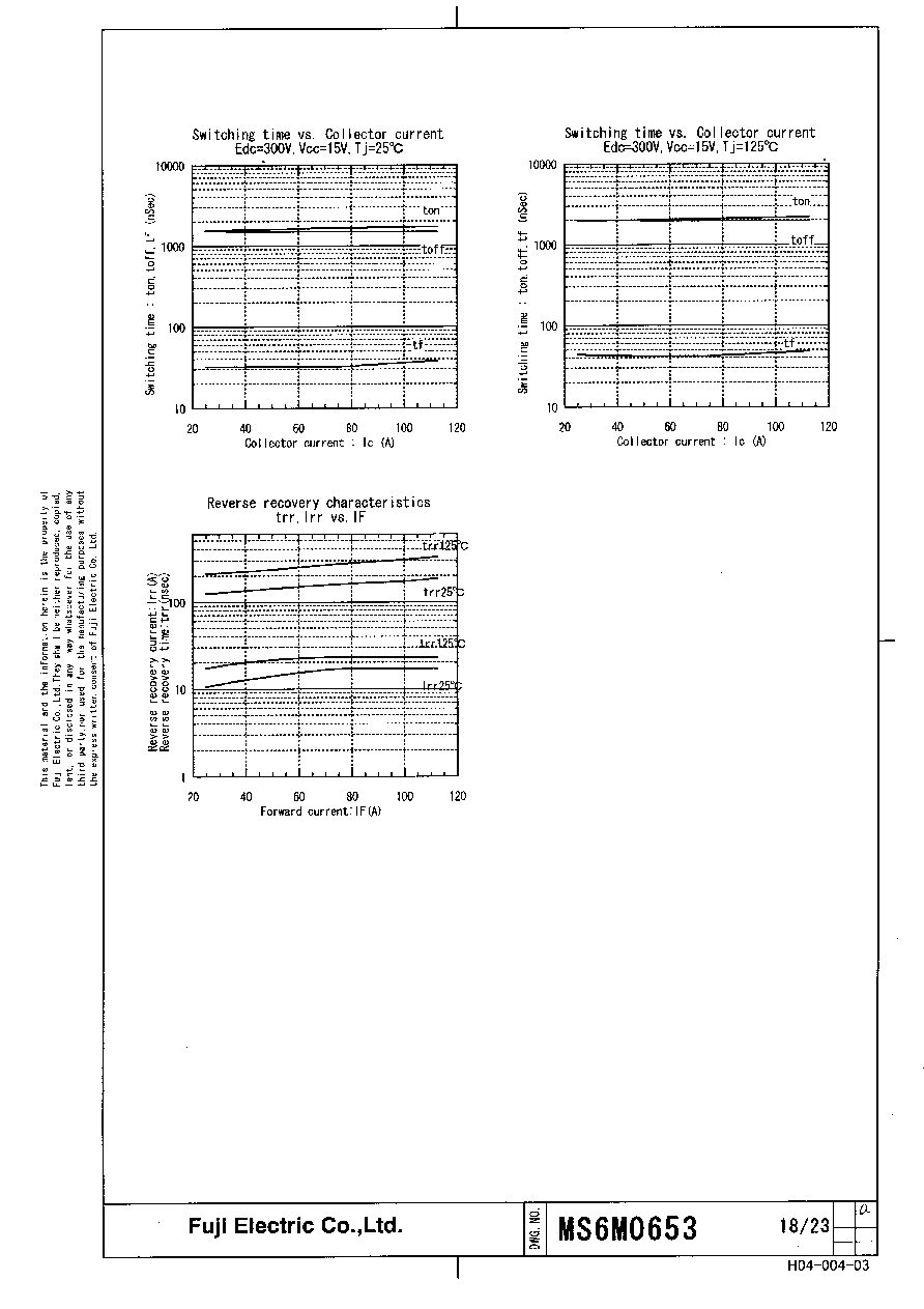
5. Electrical Characteristics
Tj25Vcc15V unless otherwise specified.
5.1 Main circuit
Symbol
Min.
Typ.
Max.
Units
Collector Current
600V
at off signal input
Vin terminal open.
Collector-Emitter
75A
Terminal
-
-
2.4
saturation voltage
Chip
-
2.0
-
V
-75A
Terminal
-
-
2.6
Chip
-
1.6
-
V
Collector Current
600V
at off signal input
Vin terminal open.
Collector-Emitter
50A
Terminal
-
-
2.2
saturation voltage
Chip
-
1.75
-
V
-50A
Terminal
-
-
3.3
Chip
-
1.9
-
V
Turn-on time
ton
V
DC
300VTj=125
1.2
-
-
Turn-off time
toff
Ic75AFig.1Fig.6
-
-
3.6
us
trr
V
DC
300V
IF75A Fig.1Fig.6
P
AV
internal wiring
Maximum AvalancheEnergy
inductance50nH
40
-
-
mJ
Main circuit wiring
inductance54nH
5.2 Control circuit
Symbol
Min.
Typ.
Max.
Units
Supply current
Switching Frequency
Supply current
Iccn
Tc-20125 Fig.7
ON
1
1.35
1.7
OFF
1.25
1.6
1.95
Input Zener Voltage
Vz
Rin20k
-
8.0
-
V
Tc-20Fig.2
1.1
-
-
Alarm Signal Hold Time
tALM
Tc25Fig.2
-
2.0
-
ms
Tc125Fig.2
-
-
4.0
Current Limit Resistor
RALM Alarm terminal
1425
1500
1575
V
CE
Forward voltage of Diode
VF
I
CES
: 015kHz
0.3
-
-
Item
Conditions
Item
Conditions
(A non-repetition)
Reverse recovery time
Forward voltage of FWD
I
CES
V
CE
VF
V
mA
mA
-
-
18
-
-
65
Vin(th)
Input signal threshold voltage
of N-side pre-driver
of P-side pre-driver (one unit)
Iccp
mA
-
-
1.0
mA
-
-
1.0
Inverter
Brake

H04-004-03
23
MS6M 0653
a
8
5.3 Protection Section Vcc
Symbol
Conditions
Min.
Typ.
Max.
Units
Over Current Protection Level
Tj=125
113
-
-
of Inverter circuit
Ioc
A
Over Current Protection Level
Tj=125
75
-
-
of Brake circuit
Over Current Protection Delay time
tdoc
Tj=125
-
5
-
us
SC Protection Delay time
tsc
Tj=125 Fig.4
-
-
8
us
IGBT Chips Over Heating
TjOH
Surface
150
-
-
Protection Temperature Level
ofIGBT Chips
Over Heating Protection Hysteresis
TjH
-
20
-
Over Heating Protection
TOH
VDC=0V,IC=0A
110
-
125
TemperatureLevel
CaseTemperature
Over Heating Protection Hysteresis
TcH
-
20
-
Under Voltage Protection Level
VUV
11
-
12.5
V
Under Voltage Protection Hysteresis
VH
0.2
0.5
-
6. Thermal Characteristics
Item
Symbol
Min.
Typ.
Max.
Units
Junction to Case
Inverter
IGBT
Rth(j-c)
-
-
0.63
Thermal Resistance *9
FWD
Rth(j-c)
-
-
0.855
/W
Brake
IGBT
Rth(j-c)
0.63
Case to Fin Thermal Resistance with Compound
Rth(c-f)
-
0.05
-
7. Noise Immunity Vdc=300VVcc=15VTest Circuit Fig 5.
Item
Conditions
Min.
Typ.
Max.
Units
Common mode
Pulse width 1us,polarity �,10 minuets
�2.0
-
-
kV
rectangular noise
Judgeno over-current, no miss operating
Common mode
Rise time 1.2us,Fall time 50usInterval 20s,10 times
�5.0
-
-
kV
lightning surge
Judgeno over-current, no miss operating
8. Recommended Operating Conditions
Item
Symbol
Min.
Typ.
Max.
Units
DC Bus Voltage
VDC
-
-
400
V
Power Supply Voltage of Pre-Driver
Vcc
13.5
15
16.5
V
Screw Torque (M5)
-
2.5
-
3
Nm
9. Weight
Item
Symbol
Min.
Typ.
Max.
Units
Weight
Wt
-
450
-
g
*9( For 1device Case is under the device )
Item

H04-004-03
23
MS6M 0653
a
9
ff
1
/Vin
Vge (Inside IPM)
Fault (Inside IPM)
/ALM
Gate Off
on
Gate On
2ms(typ.)
off
normal
t
ALM
t
ALMMax.
t
ALMMax.
off
FaultOver-current,Over-heat or Under-voltage
on
alarm
Figure 1. Switching Time Waveform Definitions
Figure 2. Input/Output Timing Diagram
Figure 3. Over-current Protection Timing Diagram
on
/Vin
Ic
/ALM
tdoc
Ioc
off
alarm
on
tdoc
Necessary conditions for alarm reset (refer to to in figure2.)
This represents the case when a failure-causing Fault lasts for a period more than tALM.
The alarm resets when the input Vin is OFF and the Fault has disappeared.
This represents the case when the ON condition of the input Vin lasts for a period more
than tALM. The alarm resets when the Vin turns OFF under no Fault conditions.
This represents the case when the Fault disappears and the Vin turns OFF within tALM.
The alarm resets after lasting for a period of the specified time tALM.
When a collector current over the OC level flows and the OFF command is input within
a period less than the trip delay time tdoc, the current is hard-interrupted and no alarm
is output.
When a collector current over the OC level flows for a period more than the trip delay
time tdoc, the current is soft-interrupted. If this is detected at the lower arm IGBTs,
an alarm is output.
Period :
Period :

H04-004-03
23
MS6M 0653
a
10
VccU
DC
15V
+
IPM
P
U
V
W
N
20k
VinU
GNDU
SW1
Vcc
DC
15V
20k
VinX
GND
SW2
Cooling
Fin
Earth
AC200V
4700p
Noise
CT
Figure 5. Noise Test Circuit
A
Vcc
Vin
GND
Icc
P
U
V
W
N
P.G
+8V
fsw
IPM
DC
15V
Figure 7. Icc Test Circuit
Figure.4 Definition of tsc
Ic
Ic
Ic
I
ALM
I
ALM
I
ALM
t
SC
Vcc
Vin
GND
DC
15V
DC
300V
N
+
L
IPM
Ic
P
HCPL-
4504
20k
Vcc
Vin
GND
DC
15V
DC
300V
N
+
L
IPM
Ic
P
HCPL-
4504
20k
Figure 6. Switching Characteristics Test Circuit

H04-004-03
23
MS6M 0653
a
11
10. Truth table
10.1 IGBT Control
The following table shows the IGBT ON/OFF status with respect to the input signal Vin.
The IGBT turn-on when Vin is at "Low" level under no alarm condition.
10.2 Fault Detection
(1) When a fault is detected at the high side, only the detected arm stops its output.
At that time the IPM dosen't any alarm.
(2) When a fault is detected at the low side, all the lower arms stop their outputs and the IP
outputs an alarm of the low side.
Alarm Output
U-phase
V-phase
W-phase
Low side
ALM
High side
OC
OFF
*
*
*
H
UV
OFF
*
*
*
H
TjOH
OFF
*
*
*
H
High side
OC
*
OFF
*
*
H
UV
*
OFF
*
*
H
TjOH
*
OFF
*
*
H
High side
OC
*
*
OFF
*
H
UV
*
*
OFF
*
H
TjOH
*
*
OFF
*
H
OC
*
*
*
OFF
L
UV
*
*
*
OFF
L
TjOH
*
*
*
OFF
L
Case
TcOH
*
*
*
OFF
L
*Depend on input logic.
Temperature
Fault
Low side
U-phase
V-phase
W-phase
Input
Output
(Vin)
(IGBT)
Low
ON
High
OFF

H04-004-03
23
MS6M 0653
a
12
11. Cautions for design and application
1. Trace routing layout should be designed with particular attention to least stray capacity
between the primary and secondary sides of optical isolators by minimizing the wiring
length between the optical isolators and the IPM input terminals as possible.
2. Mount a capacitor between Vcc and GND of each high-speed optical isolator as close to
as possible.
Vcc-GND
3. For the high-speed optical isolator, use high-CMR type one with tpHL, tpLH 0.8�s.
tpHL,tpLH0.8usCMR
4. For the alarm output circuit, use low-speed type optical isolators with CTR 100%.
CTR100%
5. For the control power Vcc, use four power supplies isolated each. And they should be
designed to reduce the voltage variations.
Vcc
6. Suppress surge voltages as possible by reducing the inductance between the DC bus P
and N, and connecting some capacitors between the P and N terminals.
P-NP-N
7. To prevent noise intrusion from the AC lines, connect a capacitor of some 4700pF between
the three-phase lines each and the ground.
AC
8. At the external circuit, never connect the control terminal GNDU to the main terminal
U-phase, GNDV to V-phase, GNDW to W-phase, and GND to N-phase. Otherwise,
malfunctions may be caused.
VVWW
N
9. Take note that an optical isolator's response to the primary input signal becomes slow
if a capacitor is connected between the input terminal and GND.
-GND

H04-004-03
23
MS6M 0653
a
13
+100m
0
Heat sink
Mounting holes
10. Taking the used isolator's CTR into account, design with a sufficient allowance to decide
the primary forward current of the optical isolator.
CTR
11. Apply thermal compound to the surfaces between the IPM and its heat sink to reduce
the thermal contact resistance.
12. Finish the heat sink surface within roughness of 10�m and flatness (camber) between scre
positions of 0 to +100�m. If the flatness is minus, the heat radiation becomes worse due to
a gap between the heat sink and the IPM. And, if the flatness is over +100�m, there is a da
that the IPM copper base may be deformed and this may cause a dielectric breakdown.
10um
0100um
IPM
100um
13. This product is designed on the assumption that it applies to an inverter use. Sufficient
examination is required when applying to a converter use. Please contact Fuji Electric Co.,
if you would like to applying to converter use.
14. Please see theFuji IGBT-IPM R SERIES APPLICATION MANUAL and Fuji IGBT
MODULES N SERIES APPLICATION MANUAL.
IGBT-IPM R IGBT N

H04-004-03
23
MS6M 0653
a
14
+
10uF
0.1uF
20k
Vcc
I
F
U
V
W
N
B
P
M
+
AC200V
+
10uF
0.1uF
20k
Vcc
I
F
+
10uF
0.1uF
Vcc
I
F
20k
+
10uF
0.1uF
20k
Vcc
I
F
+
10uF
0.1uF
20k
I
F
+
10uF
0.1uF
I
F
20k
+
0.1uF
I
F
20k
10uF
5V
1k
IPM
12. Example of applied circuit
13. Package and Marking
Please see the MT6M4140 which is packing specification of P610 & P611 & P621 package
14. Cautions for storage and transportation
Store the modules at the normal temperature and humidity (5 to 35�C, 45 to 75%).
(5354575%)
Avoid a sudden change in ambient temperature to prevent condensation on the module
surfaces.
Avoid places where corrosive gas generates or much dust exists.
Store the module terminals under unprocessed conditions
.
Avoid physical shock or falls during the transportation.
15. Scope of application
This specification is applied to the IGBT-IPM (type: 7MBP75RTB060).
IGBT-IPM (7MBP75RTB060)
16. Based safety standards
UL1557


H04-004-03
23
MS6M 0653
a
20
Test
cate-
gories
Test items
Test methods and conditions
Reference
norms
EIAJ
ED-4701
Number
of sample
Accept-
ance
number
1 Terminal strength
Pull force
: 40 N (main terminal)
Test Method 401
5
( 1 : 0 )
10 N (control terminal)
Method
(Pull test)
Test time
: 10 �1 sec.
2 Mounting Strength Screw torque
: 2.5 ~ 3.5 Nm (M5)
Test Method 402
5
( 1 : 0 )
Test time
: 10 �1 sec.
method
3 Vibration
Range of frequency
: 10500 Hz
Test Method 403
5
( 1 : 0 )
Sweeping time
: 15 min.
Condition code B
Acceleration
: 100 m/s
2
Sweeping direction
: Each X,Y,Z axis
Test time
: 6 hr. (2hr./direction)
4 Shock
Maximum acceleration : 5000 m/s
2
Test Method 404
5
( 1 : 0 )
Pulse width
1.0 ms
Condition code B
Direction
: Each X,Y,Z axis
Test time
: 3 times/direction
5 Solderabitlity
Solder temp.
: 235 �5
Test Method 303
5
( 1 : 0 )
Immersion duration
: 5.0 �0.5 sec.
Condition code A
Test time
: 1 time
Each terminal should be Immersed in solder
within 1~1.5mm from the body.
6 Resistance to
Solder temp.
: 260 �5
Test Method 302
5
( 1 : 0 )
soldering heat
Immersion time
: 10 �1sec.
Condition code A
Test time
: 1 time
Each terminal should be Immersed in solder
within 1~1.5mm from the body.
1 High temperature
Storage temp.
: 125 �5
Test Method 201
5
( 1 : 0 )
storage
Test duration
: 1000 hr.
2 Low temperature
Storage temp.
: -40 �5
Test Method 202
5
( 1 : 0 )
storage
Test duration
: 1000 hr.
3 Temperature
Storage temp.
: 85 �2
Test Method 103
5
( 1 : 0 )
humidity storage
Relative humidity
: 85 �5%
Test code C
Test duration
: 1000hr.
4 Unsaturated
Test temp.
: 120 �2
Test Method 103
5
( 1 : 0 )
pressure cooker
Atmospheric pressure : 1.7x10
5
Pa
Test code E
Test humidity
: 85 �5%
Test duration
: 96 hr.
5 Temperature
Test temp.
: Minimum storage temp. -40 �5
Test Method 105
5
( 1 : 0 )
cycle
Maximum storage temp. 125 �5
Normal temp. 5 ~ 35
Dwell time
: Tmin ~ T
N
~ Tmax ~ T
N
1hr. 0.5hr. 1hr. 0.5hr.
Number of cycles
: 100 cycles
6 Thermal shock
+0
Test Method 307
5
( 1 : 0 )
Test temp.
: High temp. side 100
-5
method
+5
Condition code A
Low temp. side 0
-0
Fluid used
: Pure water (running water)
Dipping time
: 5 min. par each temp.
Transfer time
: 10 sec.
Number of cycles
: 10 cycles
Mechanical Tests
Environment Tests
Mechanical Tests
Environment Tests
Reliability Test Items
Reliability Test Items
Reliability Test Items
Reliability Test Items
a

H04-004-03
23
MS6M 0653
a
21
Test
cate-
gories
Test items
Test methods and conditions
Reference norms
EIAJ
ED-4701
Number
of sample
Accept-
ance
number
1 High temperature
Test temp.
: Ta = 125 �5
Test Method 101
5
( 1 : 0 )
reverse bias
(Tj 150 )
Bias Voltage
: VC = 0.8�VCES
Bias Method
: Applied DC voltage to C-E
Vcc = 15V
Test duration
: 1000 hr.
2 Temperature Test
temp.
: 85
�2
Test Method 102
5
( 1 : 0 )
humidity bias
Relative humidity
: 85 �5 %
Condition code C
Bias Voltage
: VC = 0.8�VCES
Vcc = 15V
Bias Method
: Applied DC voltage to C-E
Test duration
: 1000 hr.
3 Intermitted
ON time
: 2 sec.
Test Method 106
5
( 1 : 0 )
operating life
OFF time
: 18 sec.
(Power cycle)
Test temp.
:
Tj=100 �5deg
Tj 150 , Ta=25 �5
Number of cycles
: 15000 cycles
Endurance Tests
Endurance Tests
a
Failure Criteria
Failure Criteria
Failure Criteria
Failure Criteria
Item
Characteristic
Symbol
Failure criteria
Unit
Note
Lower limit Upper limit
Electrical
Leakage current
ICES
-
USL�2
mA
characteristic
Saturation voltage
VCE(sat)
-
USL�1.2
V
Forward voltage
VF
-
USL�1.2
V
Thermal
IGBT
th(j-c)
-
USL�1.2
/W
resistance
FWD
th(j-c)
-
USL�1.2
/W
Over Current Protection
Ioc
LSL�0.8
USL�1.2
Alarm signal hold time
tALM
LSL�0.8
USL�1.2
ms
Over heating Protection
TcOH
LSL�0.8
USL�1.2
Isolation voltage
Viso
Broken insulation
-
Visual
Visual inspection
inspection
Peeling
-
The visual sample
-
Plating
and the others
LSL : Lower specified limit.
USL : Upper specified limit.
Note : Each parameter measurement read-outs shall be made after stabilizing the components at room
ambient for 2 hours minimum, 24 hours maximum after removal from the tests. And in case of the
wetting tests, for example, moisture resistance tests, each component shall be made wipe or dry
completely before the measurement.

H04-004-03
23
MS6M 0653
a
22
1. This product shall be used within its absolute maximum rating (voltage, current, and temperature).
This product may be broken in case of using beyond the ratings.
2. Connect adequate fuse or protector of circuit between three-phase line and this product to prevent
the equipment from causing secondary destruction.
3. When studying the device at a normal turn-off action, make sure that working paths of the turn-off
voltage and current are within the RBSOA specification. And ,when studying the device duty at
a short-circuit current non-repetitive interruption, make sure that the paths are also within the
avalanche proof(PAV) specification which is calculated from the snubber inductance, the IPM
inner inductance and the turn-off current. In case of use of IGBT-IPM over these specifications,
it might be possible to be broken.
RBSOA
(PAV)
4. Use this product after realizing enough working on environment and considering of product's reliability
life. This product may be broken before target life of the system in case of using beyond the product's
reliability life.
5. If the product had been used in the environment with acid, organic matter, and corrosive gas
(For example : hydrogen sulfide, sulfurous acid gas), the product's performance and appearance
can not be ensured easily.
6. The thermal stress generated from rise and fall of Tj restricts the product lifetime.
You should estimate the Tj from power losses and thermal resistance, and design the inverter lifetime
within the number of cycles provided from the power cycle curve. (Technical Rep. No.: MT6M4057)
Tj
(MT6M4057)
7. Never add mechanical stress to deform the main or control terminal.
The deformed terminal may cause poor contact problem.
Warnings

H04-004-03
23
MS6M 0653
a
23
8. According to the outline drawing, select proper length of screw for main terminal. Longer screws
may break the case.
9. If excessive static electricity is applied to the control terminals, the devices can be broken.
Implement some countermeasures against static electricity.
1. Fuji Electric is constantly making every endeavor to improve the product quality and reliability.
However, semiconductor products may rarely happen to fail or malfunction. To prevent accidents
causing injury or death, damage to property like by fire, and other social damage resulted from
a failure or malfunction of the Fuji Electric semiconductor products, take some measures to keep
safety such as redundant design, spread-fire-preventive design, and malfunction-protective design.
2. The application examples described in this specification only explain typical ones that used the Fuji
Electric products. This specification never ensure to enforce the industrial property and other rights,
nor license the enforcement rights.
3. The product described in this specification is not designed nor made for being applied to the equipment
or systems used under life-threatening situations. When you consider applying the product of this
specification to particular used, such as vehicle-mounted units, shipboard equipment, aerospace
equipment, medical devices, atomic control systems and submarine relaying equipment or systems,
please apply after confirmation of this product to be satisfied about system construction and required
reliability.
Caution
If there is any unclear matter in this specification, please contact Fuji Electric Co., Ltd.