
7MBR15NE120
IGBT Modules
IGBT MODULE
1200V / 15A / PIM
Features
∑ High Speed Switching
∑ Voltage Drive
∑ Low Inductance Module Structure
∑ Converter Diode Bridge Dynamic Brake Circuit
Applications
∑ Inverter for Motoe Drive
∑ AC and DC Servo Drive Amplifier
∑ Uninterruptible Power Supply
Maximum ratings and characteristics
Absolute maximum ratings (Tc=25∞C unless without specified)
Item Symbol Condition Ra ting Unit
Collector-Emitter voltage
Gate-Emitter voltage
Collector current
Collector power disspation
Collector-Emitter voltage
Gate-Emitter voltage
Collector current
Collector power disspation
Repetitive peak reverse voltage
Average forward current
Surge current
Repetitive peak reverse voltage
Non-Repetitive peak reverse voltage
Average output current
Surge current (Non-Repetitive)
I≤t (Non-Repetitive)
Con
v
e
r
ter Bra
k
e In
v
e
r
t
er
Operating junction temperature
Storage temperature
Isolation voltage
Mounting screw torque
V
CES
V
GES
I
C
I
CP
-I
C
P
C
V
CES
V
GES
I
C
I
CP
P
C
V
RRM
I
F(AV)
I
FSM
V
RRM
V
RSM
I
O
I
FSM
T
j
T
stg
V
iso
Continuous
1ms
1 device
Continuous
1ms
1 device
10ms
50Hz/60Hz sine wave
Tj=150∞C, 10ms
Tj=150∞C, 10ms
AC : 1 minute
1200
±20
15
30
15
120
1200
±20
10
20
88
1200
1
50
1600
1700
25
320
512
+150
-40 to +125
AC 2500
1.7 *
1
V
V
A
A
A
W
V
V
A
A
W
V
A
A
V
V
A
A
A≤s
∞C
∞C
V
N∑m
*
1
Recommendable value : 1.3 to 1.7 N∑m (M4)

Electrical characteristics (Tj=25∞C unless without specified)
Item Symbol Condition Characteristics Unit
Min. Typ. Max.
Zero gate voltage collector current
Gate-Emitter leakage current
Gate-Emitter threshold voltage
Collector-Emitter saturation voltage
Collector-Emitter voltage
Input capacitance
Switching time
Reverse recovery time of FRD
Zero gate voltage collector current
Gate-Emitter leakage current
Collector-Emitter saturation voltage
Switching time
Reverse current
Reverse recovery time
Forward voltage
Reverse current
Con
v
e
r
t
er
B
r
a
k
e
Br
a
k
e (IGBT) In
v
e
r
ter (IGBT)
(FWD)
I
CES
I
GES
V
GE(th)
V
CE(sat)
-V
CE
C
ies
t
on
t
r
t
off
t
f
t
rr
I
CES
I
GES
V
CE(sat)
t
on
t
r
t
off
t
f
I
RRM
t
rr
V
FM
I
RRM
V
CE
=1200V, V
GE
=0V
V
CE
=0V, V
GE
=±20V
V
CE
=20V, I
C
=15mA
V
GE
=15V, Ic=15A
-Ic=15A
V
GE
=0V, V
CE
=10V, f=1MHz
V
CC
=600V
I
C
=15A
V
GE
=±15V
R
G
=82 ohm
I
F
=15A
V
CES
=1200V, V
GE
=0V
V
CE
=0V, V
GE
=±20V
I
C
=10A, V
GE
=15V
V
CC
=600V
I
C
=10A
V
GE
=±15V
R
G
=120 ohm
V
R
=1200V
I
F
=25A
V
R
=1600V
1.0
20
7.5
3.3
3.0
1.2
0.6
1.5
0.5
0.35
1.0
0.1
3.3
0.8
0.6
1.5
0.5
1
0.6
1.4
1.0
2400
4.5
mA
µA
V
V
V
pF
µs
µs
µs
µs
µs
mA
µA
V
µs
µs
µs
µs
mA
µs
V
mA
Item Symbol Condition Characteristics Unit
Min. Typ. Max.
Inverter IGBT
Inverter FRD
Brake IGBT
Converter Diode
With thermal compound
1.04
2.78
1.43 ∞C/W
3.40
0.05
Thermal resistance ( 1 device ) Rth(j-c)
Contact thermal resistance * Rth(c-f)
Thermal Characteristics
IGBT Module
7MBR15NE120
* This is the value which is defined mounting on the additional cooling fin with thermal compound
Equivalent Circuit Schematic
*
NLU (Over current Limiting circuit)

IGBT Module
7MBR15NE120
Collector current vs. Collector-Emitter voltage
Tj=25∞C
Collector current vs. Collector-Emitter voltage
Tj=125∞C
Collector-Emitter vs. Gate-Emitter voltage
Tj=25∞C
Collector-Emitter vs. Gate-Emitter voltage
Tj=125∞C
Switching time vs. Collector current
Vcc=600V, RG=82 ohm, VGE=±15V, Tj=25∞C
Switching time vs. Collector current
Vcc=600V, RG=82 ohm, VGE=±15V, Tj=125∞C
Collector-Emitter voltage : VCE [V]
Collector-Emitter voltage : VCE [V]
Collector current : Ic [A]
Collector current : Ic [A]
20
10
0
0
0 1 2 3 4 5
0 1 2 3 4 5
Collector-Emitter v
oltage :
VCE [V]
Collector-Emitter v
oltage :
VCE [V]
10
8
6
4
2
0
0 5 10 15 20 25
0 5 10 15 20 25
10
8
6
4
2
0
Gate-Emitter voltage : VGE [V]
Gate-Emitter voltage : VGE [V]
Switching time :
ton, tr
, toff
, tf [n sec.]
1000
100
10
0 10 20 30
Collector current : Ic [A]
Collector current : Ic [A]
Switching time :
ton, tr
, toff
, tf [n sec.]
1000
100
10
20
10
30
30
0 10 20 30
Characteristics (Representative)
Inverter

IGBT Module
7MBR15NE120
Switching time vs. RG
Vcc=600V, Ic=15A, VGE=±15V, Tj=25∞C
Dynamic input characteristics
Tj=25∞C
Gate resistance : RG [ohm]
100
Gate charge : Qg [nC]
0 50 100 150 200 250 300
100
1000
1000
800
600
400
200
0
Switching time :
ton, tr
, toff
, tf [n sec.]
Collector-Emitter v
o
ltage :
VCE [V]
F
orward current :
IF [A]
20
10
0
0 1 2 3 4 5
Gate-Emitter v
oltage :
V
GE [V]
0
5
15
20
25
Forward voltage : VF [V]
Re
v
erse reco
v
e
r
y
current :
Irr [A]
Re
v
erse reco
v
e
r
y
time :
trr [n sec.]
Forward current vs. Forward voltage
VGE=0V
Reverse recovery characteristics
trr, Irr, vs. IF
Forward current : IF [A]
10
100
1
Ther
mal resistance :
Rth (j-c) [∞C/W]
Transient thermal resistance
0.1
1
0.001 0.01 0.1 1
Pulse width : PW [sec.]
Reversed biased safe operating area
+VGE=15V, -VGE = 15V, Tj = 125∞C, RG = 82 ohm
0 5 10 15 20
<
<
>
100
80
60
40
20
0
0 200 400 600 800 1000 1200
Collector-Emitter voltage : VCE [V]
Collector current : Ic [A]
10
30
0.01
120
140

IGBT Module
7MBR15NE120
Switching loss vs. Collector current
Vcc=600V, RG=82 ohm, VGE=±15V
Switching loss :
Eon, Eoff
, Err [mJ /cycle]
Collector current : Ic [A]
0
2
1
3
4
0 5 10 15 20 25 30
Collector-Emitter voltage : VCE [V]
0 5 10 15 20 25 30 35
0.1
1
10
Capacitance :
Cies, Coes
, Cres [nF]
Capacitance vs. Collector-Emitter voltage
Tj=25∞C
F
orward current :
IF [A]
30
25
20
15
10
5
0
0 0.5 1.0 1.5 2.0
Forward voltage : VF [V]
Converter Diode
Forward current vs. Forward voltage
5
6

IGBT Module
7MBR15NE120
Collector current vs. Collector-Emitter voltage
Tj=25∞C
Collector current vs. Collector-Emitter voltage
Tj=125∞C
Collector-Emitter vs. Gate-Emitter voltage
Tj=25∞C
Collector-Emitter vs. Gate-Emitter voltage
Tj=125∞C
Switching time vs. Collector current
Vcc=600V, RG=120 ohm, VGE=±15V, Tj=25∞C
Switching time vs. Collector current
Vcc=600V, RG=120 ohm, VGE=±15V, Tj=125∞C
Collector-Emitter voltage : VCE [V]
Collector-Emitter voltage : VCE [V]
Collector current : Ic [A]
Collector current : Ic [A]
25
20
15
10
5
0
0
0 1 2 3 4 5
0 1 2 3 4 5
Collector-Emitter v
oltage :
VCE [V]
Collector-Emitter v
oltage :
VCE [V]
10
8
6
4
2
0
0 5 10 15 20 25
0 5 10 15 20 25
10
8
6
4
2
0
Gate-Emitter voltage : VGE [V]
Gate-Emitter voltage : VGE [V]
Switching time :
ton, tr
, toff
, tf [n sec.]
1000
100
10
0 5 10 15 20
Collector current : Ic [A]
Collector current : Ic [A]
Switching time :
ton, tr
, toff
, tf [n sec.]
1000
100
10
25
20
15
10
5
Brake
0 5 10 15 20

IGBT Module
7MBR15NE120
Switching loss vs. Collector current
Vcc=600V, RG=120 ohm, VGE=±15V
Switching loss :
Eon, Eoff
, Err [mJ /cycle]
Collector current : Ic [A]
0
1
0 5 10 15 20
Collector-Emitter voltage : VCE [V]
0 5 10 15 20 25 30 35
0.1
1
Capacitance :
Cies, Coes
, Cres [nF]
Capacitance vs. Collector-Emitter voltage
Tj=25∞C
Switching time vs. RG
Vcc=600V, Ic=10A, VGE=±15V, Tj=25∞C
Dynamic input characteristics
Tj=25∞C
Gate resistance : RG [ohm]
Gate charge : Qg [nC]
0 50 100 150 200
100
1000
1000
800
600
400
200
0
Switching time :
ton, tr
, toff
, tf [n sec.]
Collector-Emitter v
oltage :
VCE [V]
Gate-Emitter v
oltage :
V
GE [V]
0
5
10
15
20
25
Reversed biased safe operating area
+VGE=15V, -VGE = 15V, Tj = 125∞C, RG = 120 ohm
<
<
>
100
80
60
40
20
0
0 200 400 600 800 1000 1200
Collector-Emitter voltage : VCE [V]
Collector current : Ic [A]
100
1000
2
3
4
10
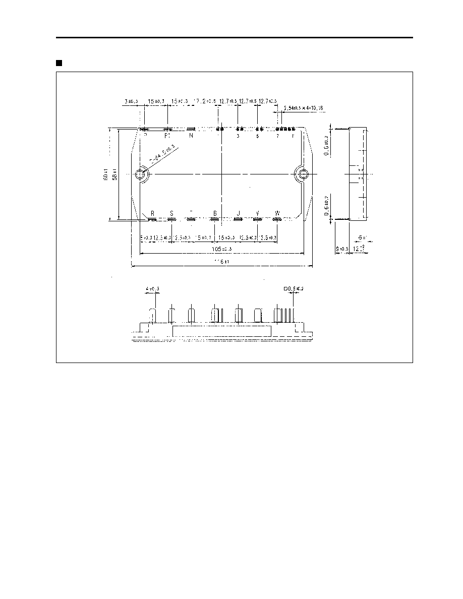
IGBT Module
7MBR15NE120
Outline Drawings, mm

For more information, contact:
Collmer Semiconductor, Inc.
P.O. Box 702708
Dallas, TX 75370
972-733-1700
972-381-9991 Fax
http://www.collmer.com