 | –≠–ª–µ–∫—Ç—Ä–æ–Ω–Ω—ã–π –∫–æ–º–ø–æ–Ω–µ–Ω—Ç: FA3635P | –°–∫–∞—á–∞—Ç—å:  PDF PDF  ZIP ZIP |
FA3635P
1
FA3635P
s
Description
FA3635P is a CMOS IC which includes low on-resistance
power MOSFET for PWM-type switching power supply control.
This IC achieves high efficiency DC-DC converter and it is
suitable for buck converter or inverting converter with high
input voltage of 10V to 50V.
s
Features
∑ Built-in low on-resistance Pch power MOSFET
50V/1.1
(typ.)/1A(peak)
∑ Wide range of 10V to 50V for input voltage
∑ 1.2mA low operating current as a Power IC
∑ Latch-mode short-circuit protection function
∑ Built-in over-temperature protection
Tj =125
∞
C (min.)
s
Applications
∑ Power supply for general equipment
s
Dimensions, mm
DIP-8
1
8
5
4
9.4
6.5
7.6
3.4
4.5max
1.5
3.1min
0~15∞
0~15∞
0.5
±
0.1
2.54
±
0.25
0.25
+0.1
≠0.05
s
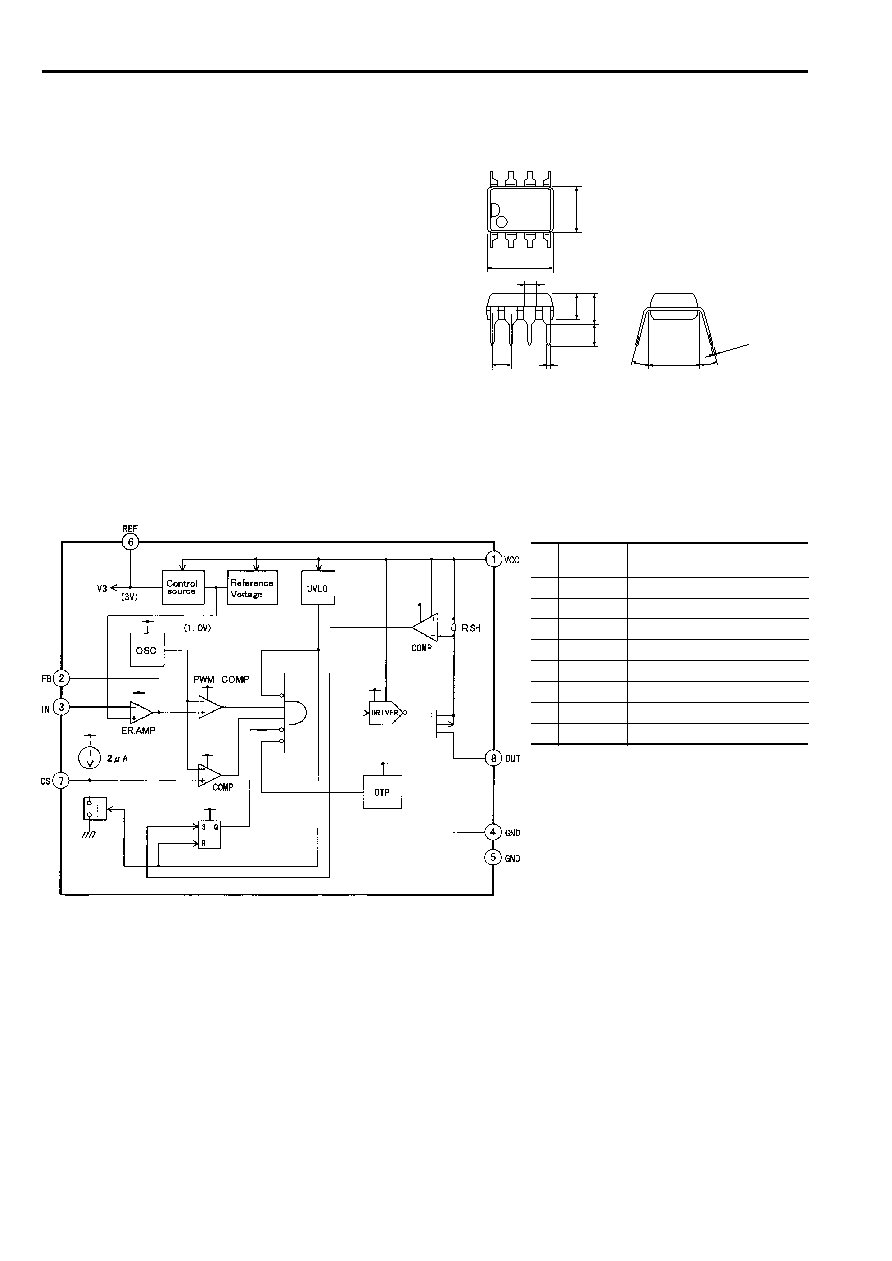
Block diagram
CMOS IC
For Switching Power Supply Control
Pin
Pin
Description
No.
symbol
1
VCC
Power supply
2
FB
Error amplifier output
3
IN
Inverting input to error amplifier
4
GND
Ground
5
GND
Ground
6
REF
Reference voltage
7
CS
Capacitor for soft-start
8
OUT
Output
FA3635P
2
s
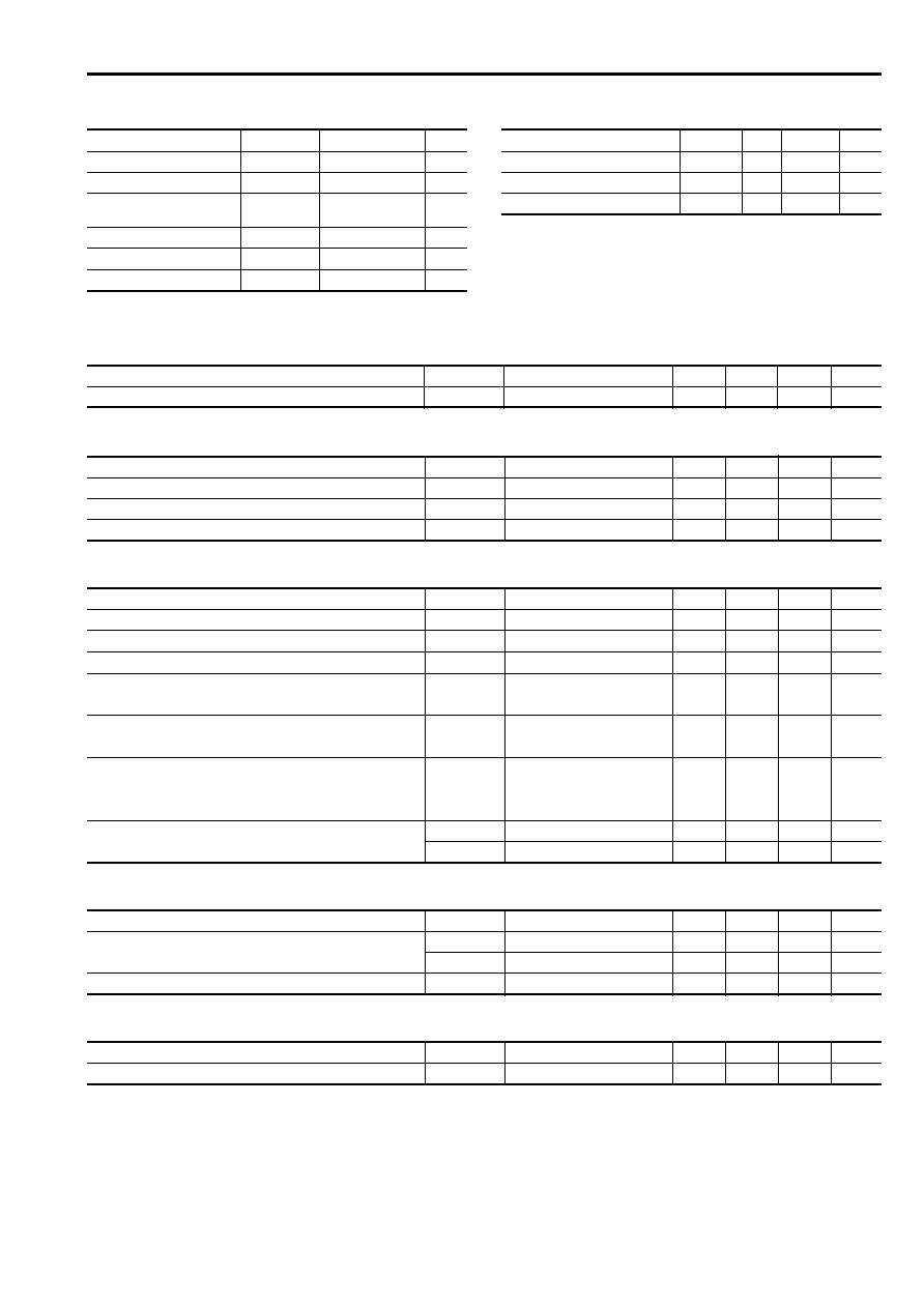
Electrical characteristics (Ta=25
∞
C, V
CC
=44V, C
REF
=0.1
µ
F)
Reference voltage section
Item
Symbol
Test condition
Min.
Typ.
Max.
Unit
terminal Voltage
V
REG
C
REF
=0.1
µ
F
3.00
3.12
3.24
V
Oscillator section
Item
Symbol
Test condition
Min.
Typ.
Max.
Unit
Oscillation frequency
f
OSC
70
81
100
kHz
Frequency change with supply voltage
f
dV
V
CC
=10 to 45V
±
1
±
3
%
Frequency change with temperature
f
dT
T
a=≠20 to +85
∞
C
±
3
±
5
%
Error amplifier section
Item
Symbol
Test condition
Min.
Typ.
Max.
Unit
Input common mode voltage range
V
ICOM
0.2
2.5
V
Open-loop gain
A
VOL
55
dB
Unity-gain bandwidth
f
T
1.0
MHz
Output sink current
I
FBL
Voltage follower
3.0
3.8
mA
V
FB
=
V
ref
+0.05V
Output source current
I
FBH
Voltage follower
≠140
≠100
µ
A
V
FB
=
V
ref
≠0.05V
Reference Voltage
V
ref
Voltage follower
0.97
1.00
1.03
V
V
CC
=10 to 45V
T
a=≠20 to +85
∞
C
Input threshold voltage (Pin 2)
V
FB 0
Duty cycle=0%
0.5
0.6
0.7
V
V
FB 100
Duty cycle=100%
2.3
2.5
2.7
V
Undervoltage lockout circuit section
Item
Symbol
Test condition
Min.
Typ.
Max.
Unit
Operating voltage
V
UVLO
5.0
6.1
8.5
V
Soft-start circuit section
Item
Symbol
Test condition
Min.
Typ.
Max.
Unit
Input threshold voltage (Pin 7)
V
CS 0
Duty cycle=0%
0.5
0.6
0.7
V
V
CS 100
Duty cycle=100%
2.3
2.5
2.7
V
Charge current
I
CS
≠2.8
≠2.2
≠1.6
µ
A
s
Recommended operating conditions
Item
Symbol
Min.
Max.
Unit
Supply voltage
V
CC
10.0
45.0
V
REF terminal by-pass capacitor
C
REF
0.047 0.22
µ
F
VCC terminal by-pass capacitor
C
O
470
µ
F
s
Absolute maximum ratings
Item
Symbol
Rating
Unit
V
CC
50.0
V
V
IN
5.5
V
P
d
1.1
W
T
j
125
∞
C
Operating temperature
T
op
≠20 to +85
∞
C
∞
C
Storage temperature
T
stg
≠40 to +150
∞
C
Supply voltage
Error amplifier input voltage
Total Power dissipation
(Ta = 25
∞
C)
Junction temperature

FA3635P
3
Output section
Item
Symbol
Test condition
Min.
Typ.
Max.
Unit
Voltage drop
V
DROP
I
OUT
=1.0A
1.1
1.4
V
I
OUT
=0.7A
0.7
0.9
I
OUT
=0.1A
0.1
0.2
Overcurrent limit
I
OLMT
Peak current
1.0
1.75
2.0
A
s
Characteristic curve
Thermal characteristic
Ambient temperature [
∞
C]
L
OSS
[W]
0.2
0.4
0.6
0.8
1.2
1.4
1.6
1
0
0
50
100
150
Overall device
Item
Symbol
Test condition
Min.
Typ.
Max.
Unit
Operating current
I
CC
Out pin open,
V
CC
=44V
0.9
4.0
mA
Duty cycle=100%
Thermal resistance :
j-c(Junction to case) = 30
∞
C/W
j-a(Junction to air) = 90
∞
C/W
Overheat protection section
Item
Symbol
Test condition
Min.
Typ.
Max.
Unit
Operating temperature
T
OH
125
135
145
∞
C
Hysteresis width
T
OH
45
50
55
∞
C
FA3635P
4
s
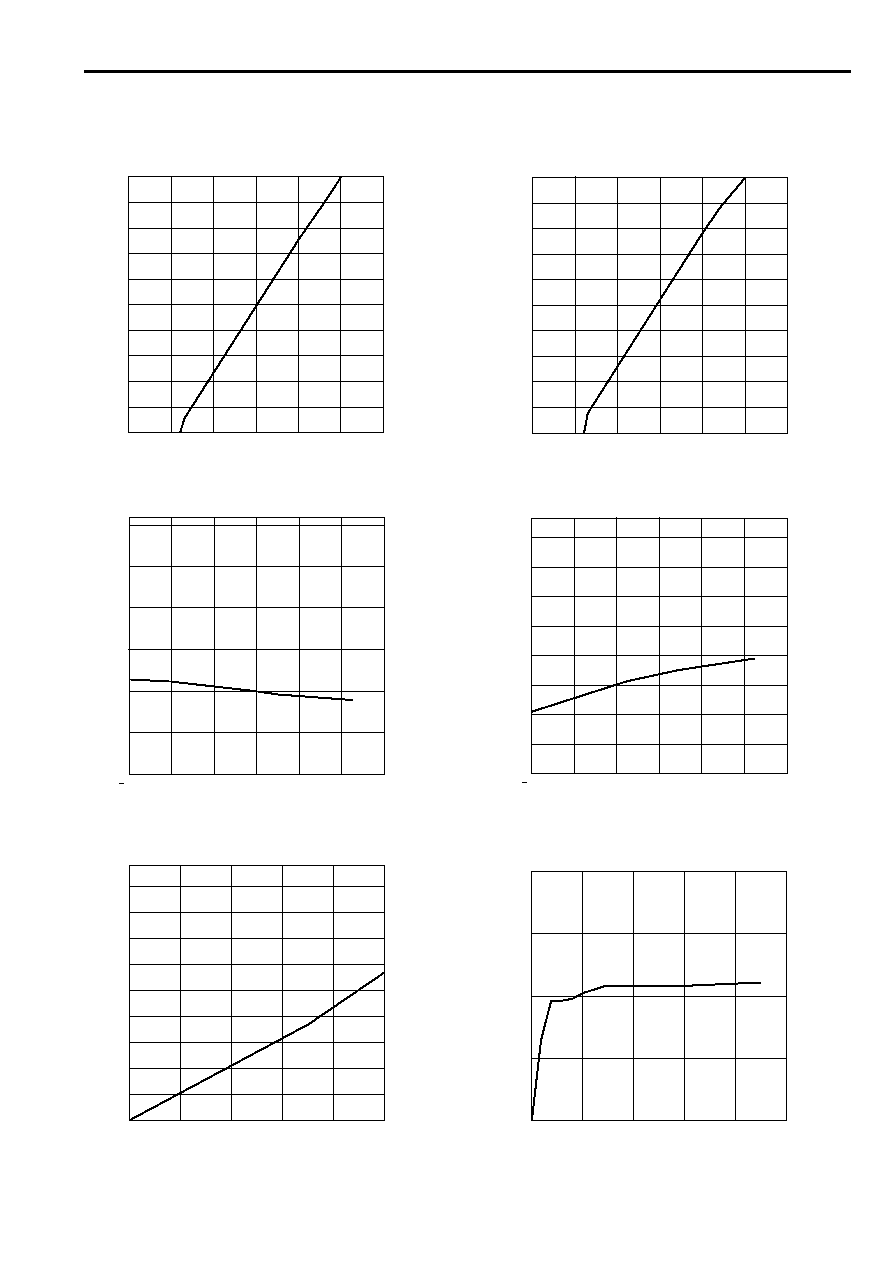
Characteristic curves (Ta=25
∞
C)
Output duty cycle vs. FB terminal voltage (V
FB
)
Output duty cycle vs. CS terminal voltage (V
CS
)
0
0.5
1
1.5
2
2.5
3
0
10
20
30
40
50
60
70
80
90
100
V
FB
[V]
Output duty cycle [%]
Oscillation frequency (f
OSC
) vs. ambient temperature (T
a
)
Reference voltage (V
REF
) vs. ambient temperature (T
a
)
Ta [
∞
C]
fosc [kHz]
75
80
85
90
95
100
70
0
20
40
60
80
100
20
Output voltage (V
OUT
) vs. output current (I
OUT
)
Supply current (I
CC
) vs. supply voltage (V
CC
)
I
OUT
[A]
0.2
0.4
0.6
0.8
1
1.2
1.4
1.6
1.8
0
0
0.2
0.4
0.6
0.8
1
V
CC≠
V
OUT
[V]
0
0.5
1
1.5
2
2.5
3
0
10
20
30
40
50
60
70
80
90
100
V
CS
[V]
Output duty cycle [%]
V
REF
[V]
0.97
0.98
0.99
1
1.01
1.02
1.03
1.04
1.05
Ta [
∞
C]
0
20
40
60
80
100
20
Vcc [V]
Icc [mA]
0
0.5
1.5
2
1
0
10
20
30
40
50
FA3635P
5
s
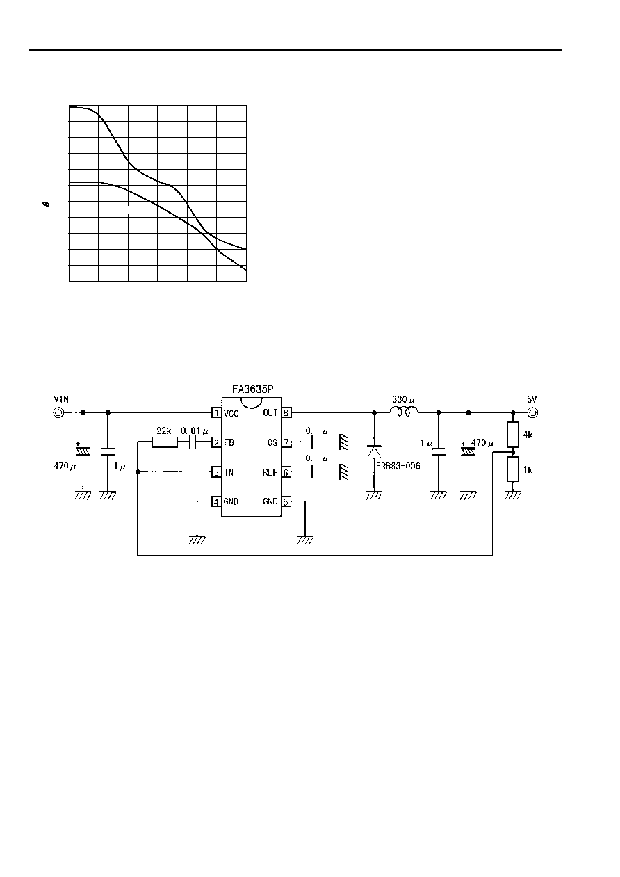
Application circuit
Error amplifier voltage gain (A
V
)/ phase (
) vs. frequency (f)
Condition: Open loop
[H
Z
]
[deg]
A
v
[dB]
0
20
40
60
80
100
120
140
160
180
10
100
10K
1K
100K
1M
10M
≠ 40
≠ 20
Voltage gain
Phase
Parts tolerances characteristics are not defined in the circuit design
sample shown above. When designing an actual circuit for a product,
you must determine parts tolerances and characteristics for safe and
economical operation.