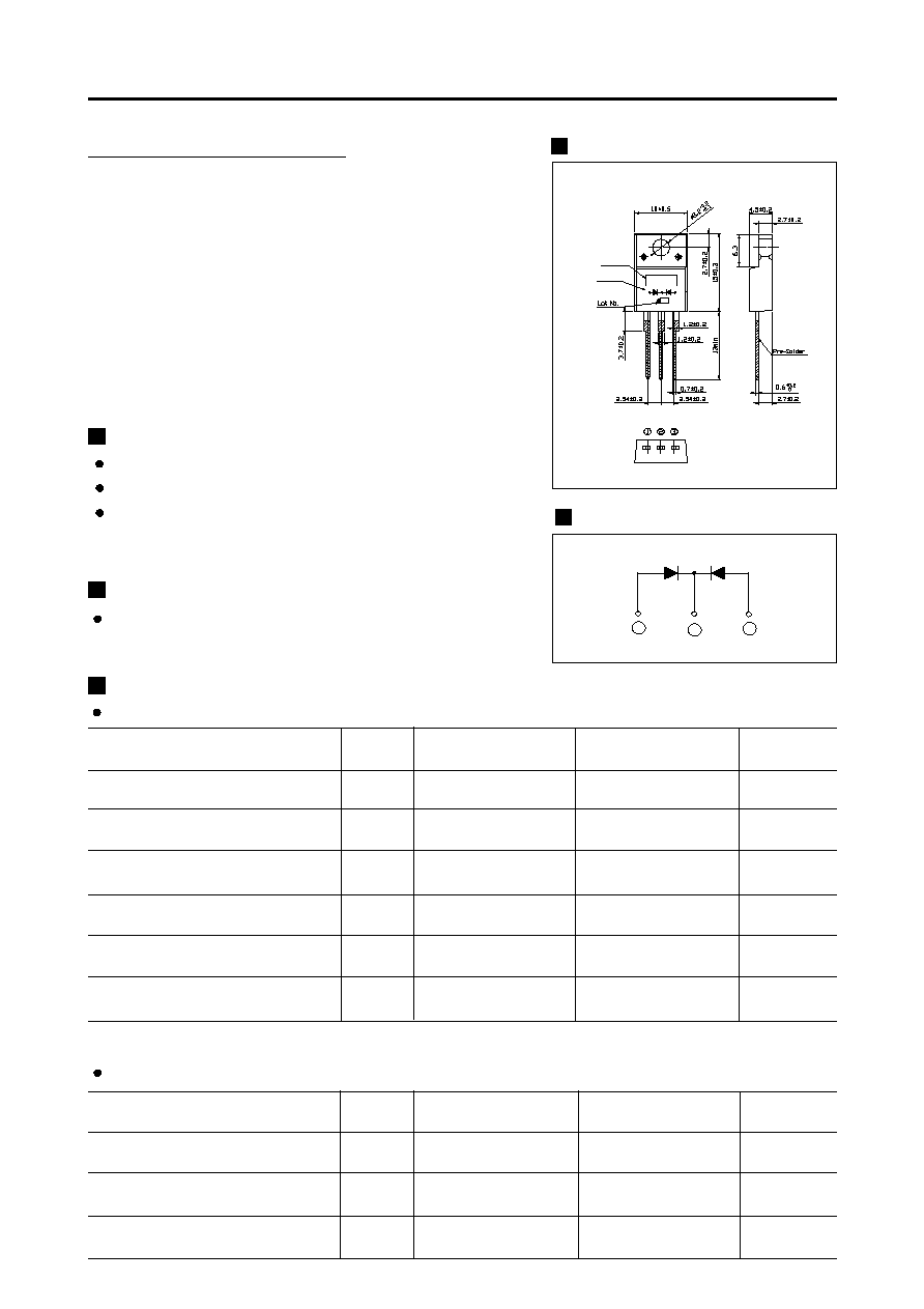
Type name
Polarity mark
TO-220F
YG838C03R
(30A)
(30V / 30A )
Features
Low V
F
Super high speed switching
High reliability by planer design
Applications
High speed power switching
Maximum ratings and characteristics
Absolute maximum ratings
Item
Repetitive peak reverse voltage
Repetitive peak surgereverse voltage
Average output current
Surge current
Operating junction temperature
Storage temperature
Symbol
V
RRM
V
RSM
I
o
I
FSM
T
j
T
stg
Conditions
Sine wave
10ms
180
-40 to +150
-40 to +150
Unit
V
V
A
A
∞C
∞C
Electrical characteristics (Ta=25∞C Unless otherwise specified )
Item
Forward voltage drop
Reverse current
Thermal resistance
Symbol
V
FM
I
RRM
R
th(j-c)
Conditions
I
FM
=12.5A
V
R
=V
RRM
Junction to case
Max.
0.53
8
2.0
Unit
V
mA
∞C/W
tw=500ns, duty=
1/40
Square wave, duty=
1/2
Tc=85∞C
Rating
30
35
30*
SCHOTTKY BARRIER DIODE
Outline drawings, mm
Connection diagram
1
3
2
*
Average forward current of centertap full wave connection

YG838C04R (30A)
(40V / 30A )
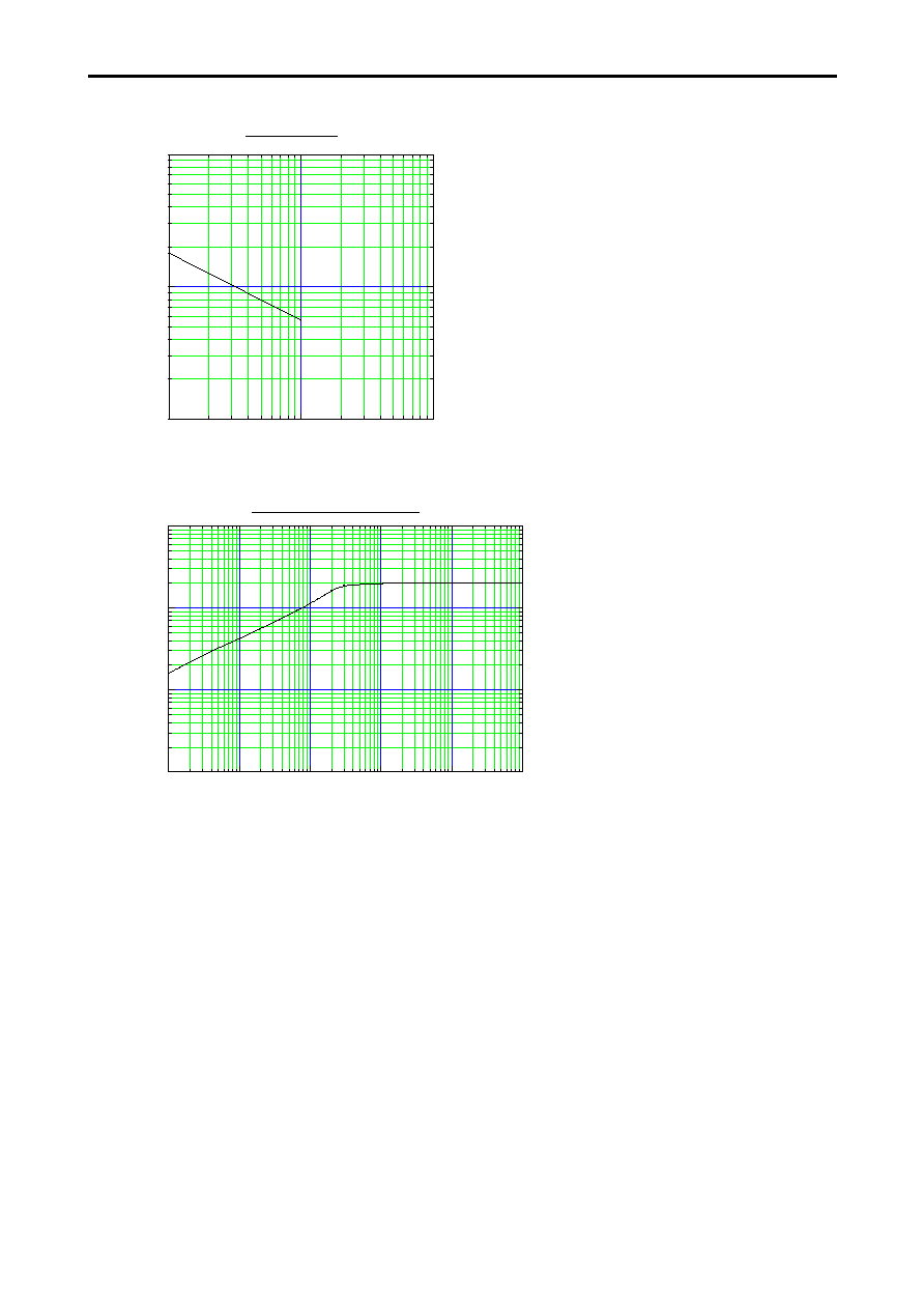
Characteristics
0.1
1
10
100
0.0 0.1 0.2 0.3 0.4 0.5 0.6 0.7 0.8 0.9 1.0 1.1 1.2
Tj=150∞C
Tj=125∞C
Tj=100∞C
Tj=25∞C
Forward Characteristic (typ.)
IF Forward Current (A)
VF Forward Voltage (V)
0
10
20
30
40
50
10
-2
10
-1
10
0
10
1
10
2
10
3
Reverse Characteristic (typ.)
Tj= 25∞C
Tj=100∞C
Tj=125∞C
Tj=150∞C
IR Reverse Current (mA)
VR Reverse Voltage (V)
0
2
4
6
8
10
12
14
16
0
2
4
6
8
10
12
14
16
18
20
22
Per 1element
DC
Square wave
=180∞
Sine wave
=180∞
Square wave
=120∞
Square wave
=60∞
Forward Power Dissipation
WF Forward Power Dissipation (W)
Io Average Forward Current (A)
360∞
Io
-5
0
5
10
15
20
25
30
35
40
45
0
2
4
6
8
10
12
14
16
18
20
22
24
26
28
30
32
34
36
38
Reverse Power Dissipation
=180∞
DC
PR Reverse Power Dissipation (W)
VR Reverse Voltage (V)
360∞
VR
0
5
10
15
20
25
30
35
40
45
30
40
50
60
70
80
90
100
110
120
130
140
150
160
:Conduction angle of forward current for each rectifier element
Io:Output current of center-tap full wave connection
Square wave
=120∞
Square wave
=60∞
Square wave
=180∞
Sine wave
=180∞
DC
Current Derating (Io-Tc)
Tc Case Temperature (∞C)
Io Average Output Current (A)
VR=30V
360∞
Io
1
10
100
10
100
1000
10000
Junction Capacitance Characteristic (typ.)
Cj Junction Capacitance (pF)
VR Reverse Voltage (V)
YG838C04R (30A)
(40V / 30A )
1
10
100
10
100
1000
Surge Capability
I FSM Peak Half - Wave Current (A)
Number of Cycles at 50Hz
10
-3
10
-2
10
-1
10
0
10
1
10
2
10
-2
10
-1
10
0
10
1
Transient Thermal Impedance
Transient Thermal Impedance (∞C/W)
t Time (sec.)