DS04-28203-4E
FUJITSU SEMICONDUCTOR
DATA SHEET
ASSP Image Processing
BIPOLAR
A/D Converter
(1-channel, 8-bit low-power model with built-in clamp circuit)
MB40568
s
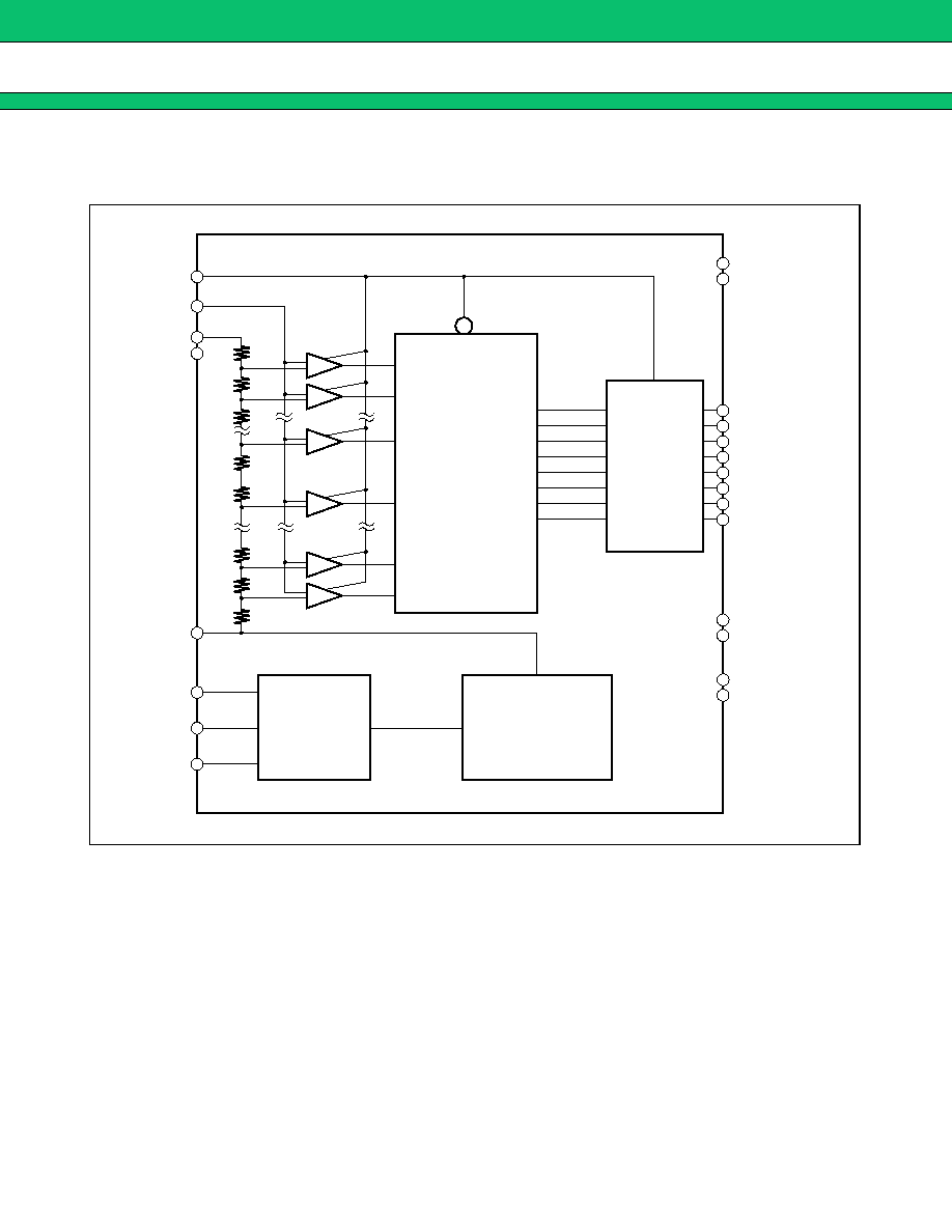
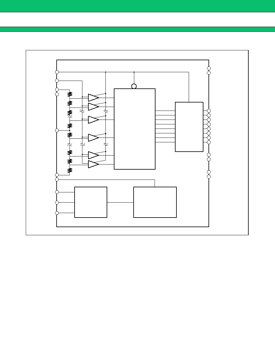
DESCRIPTION
The MB40568 is an all-parallel (flash type) A/D converter for 8-bit video applications, and uses high-speed bipolar
process technology for low-power consumption and high-speed conversion.
This A/D converter is capable of converting analog signals into digital signals at a rate of DC to 20 MSPS
(megasamples per second). Additional circuitry including a clamp circuit and reference voltage generator circuits
are build in, to make the MB40568 ideally suited for video signal processing.
s
FEATURES
∑ Resolution: 8 bits
∑ Linearity error: ±0.15 % typ.
∑ Maximum conversion rate: 20 MSPS min.
∑ Analog input voltage: 0 to 3 V in 2 V
P-P
(clamp circuit)
3 to 5 V (without clamp circuit)
∑ Digital input/output level: TTL Levels
∑ Power supply voltage: +5 V single power supply
∑ Power dissipation: 200 mW typ.
s
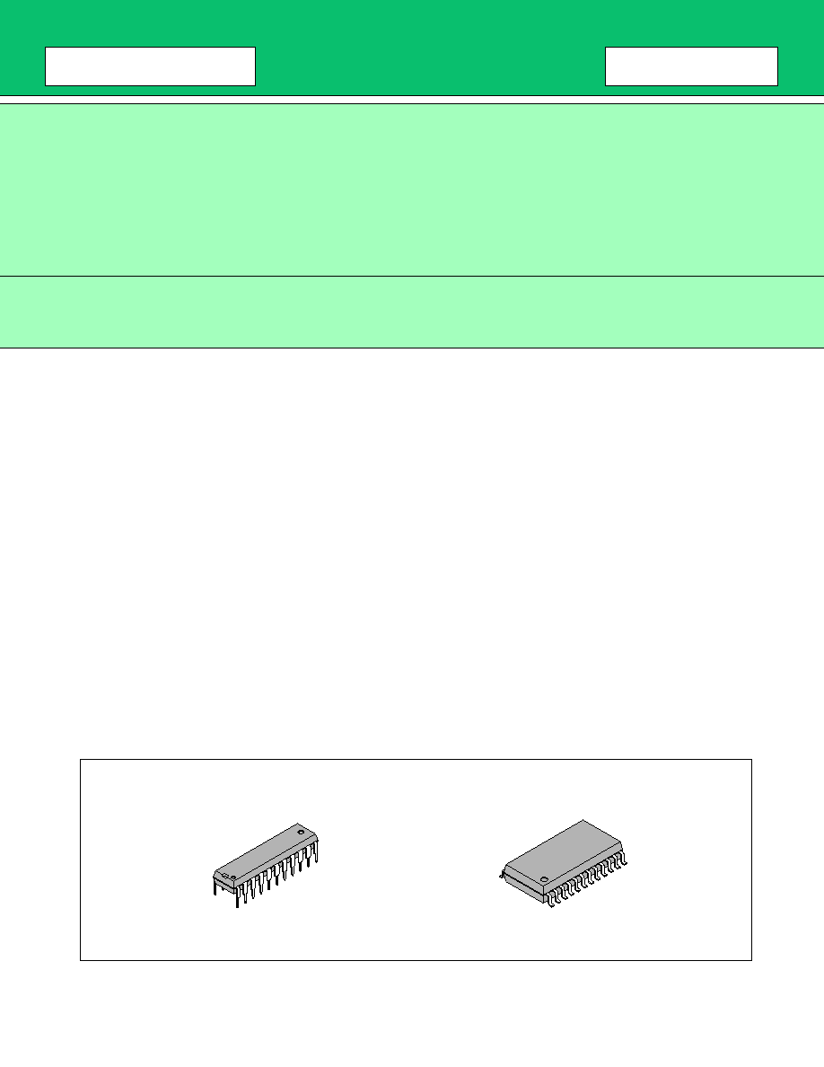
PACKAGES
22-pin Plastic SK-DIP
(DIP-22P-M04)
24-pin Plastic SOP
(FPT-24P-M02)
2
MB40568
s
PIN ASSIGNMENTS
s
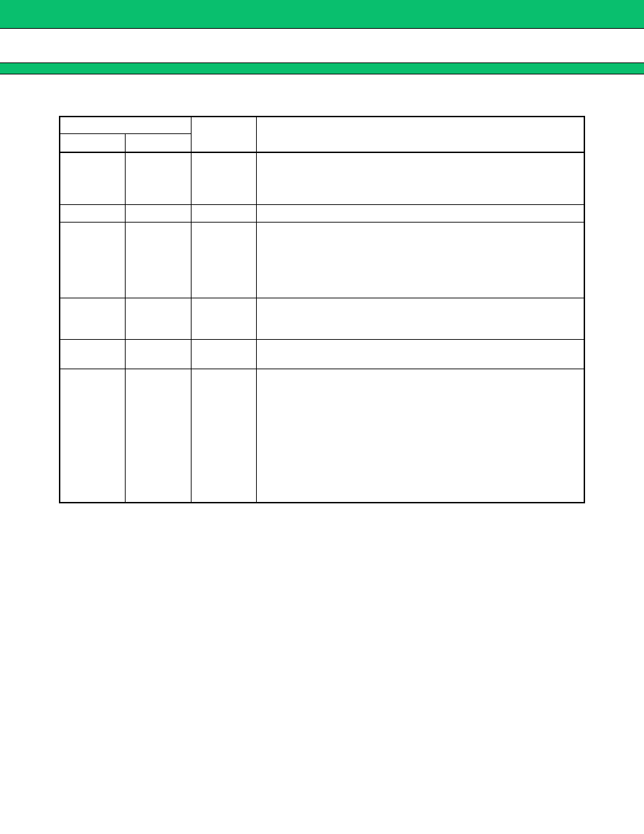
PIN DESCRIPTIONS
(Continued)
Pin no.
Symbol
Function
DIP
SOP
1, 11
1, 11
D.GND
Ground pin
Should be connected to the analog system ground.
2 to 9
2 to 9
D
8
to D
1
Digital signal output pin
10
10
CLK
Clock input pin
12, 22
12, 24
A.GND
Ground pin
Should be connected to the analog system ground.
13, 21
13, 23
V
CCD
Power supply voltage input pin
Also functions as V
CCA
power supply, and should be in the same
voltage level as V
CCA
pin.
14, 20
14, 22
V
CCA
Power supply voltage input pin
Also functions as V
CCD
power supply, and should be in the same
voltage level as V
CCD
pin.
15
15
V
INC
Clamp circuit input pin
The clamp circuit is a diode-clamp type sync chip clamp circuit.
Should be shorted to ground if the clamp circuit is not used.
16
16
V
OUTC
Clamp circuit output pin
A capacitor of at least 1
µ
F should be connected between this pin
and the V
CLMP
pin.
Should be left open if the clamp circuit is not used.
D.GND
D
8
(LSB)
D
7
D
6
D
5
D
4
D
3
D
2
D
1
(MSB)
CLK
D.GND
1
2
3
4
5
6
7
8
9
10
11
22
21
20
19
18
17
16
15
14
13
12
A.GND
V
CCD
V
CCA
V
RB
V
INA
V
CLMP
V
OUTC
V
INC
V
CCA
V
CCD
A.GND
(Top view)
(DIP-22P-M04)
(FPT-24P-M02)
D.GND
D
8
(LSB)
D
7
D
6
D
5
D
4
D
3
D
2
D
1
(MSB)
CLK
D.GND
A.GND
1
2
3
4
5
6
7
8
9
10
11
12
24
23
22
21
20
19
18
17
16
15
14
13
A.GND
V
CCD
V
CCA
V
RB
V
REF
V
RM
V
INA
V
CLMP
V
OUTC
V
INC
V
CCA
V
CCD
(Top view)
3
MB40568
(Continued)
Pin no.
Symbol
Function
DIP
SOP
17
17
V
CLMP
Clamp voltage output pin
A capacitor of at least 1
µ
F should be connected between this pin
and the V
OUTC
pin.
Should be left open if the clamp circuit is not used.
18
18
V
INA
Analog signal input pin
19
--
V
RB
Analog reference voltage pin
In the DIP model, this pin is internally connected to the reference
circuit.
Always be sure that a capacitor is connected immediately next to the
IC, between this pin and the ground. The capacitor must be at least
1
µ
F with excellent frequency characteristics.
--
19
V
RM
Reference voltage monitor pin
Set to the midpoint of resistance between V
CCA
and V
RB
.
Should be left open in normal use.
--
20
V
REF
Reference voltage output pin
Should be left open when no reference voltage source is used.
--
21
V
RB
Analog reference voltage input pin
When an internal reference voltage source is used, this pin should
be shorted to the V
REF
pin. In this case, always be sure that a
capacitor is connected immediately next to the IC, between this pin
and the ground. The capacitor must be at least 1
µ
F with excellent
frequency characteristics.
When an external reference voltage source is used, this pin will
carry a current of up to 8.5 mA, therefore it is necessary to use a
voltage source with sufficient sync capacity.
A capacitor connection should also be used similar to that used with
internal reference voltage sources.