1.5KA6.8 THRU 1.5KA43A
AUTOMOTIVE TRANSIENT VOLTAGE SUPPRESSOR
Breakdown Voltage - 6.8 to 43 Volts Peak Pulse Power - 1500 Watts
FEATURES
Designed for under the hood applications
Plastic package has Underwriters Laboratory
Flammability Classification 94V-0
1500W peak pulse power surge capability with a
10/1000
µ
s waveform, repetition rate (duty cycle): 0.01%
Exclusive patented PARTM oxide passivated
chip construction
Excellent clamping capability
Low incremental surge resistance
Fast response time: typically less
than 1.0 ps from 0 Volts to V
(BR)
for uni-directional
For devices with V
(BR)
10V I
D
are typically less than
1.0
µ
A at T
A
=150∞C
High temperature soldering guaranteed:
300∞C/10 seconds, 0.375" (9.5mm) lead length,
5lbs. (2.3 kg) tension
MECHANICAL DATA
Case: Molded plastic over passivated junction
Terminals: Solder plated axial leads, solderable per
MIL-STD-750, Method 2026
Polarity: Color band denotes positive end (cathode)
Mounting Position: Any
Weight: 0.045 ounce, 1.2 grams
MAXIMUM RATINGS AND CHARACTERISTICS
Ratings at 25∞C ambient temperature unless otherwise specified.
SYMBOL
VALUE
UNITS
Peak pulse power dissipation with a 10/1000
µ
s waveform
(NOTE 1, FIG. 1)
P
PPM
Minimum 1500
Watts
Peak pulse current at T
A
=25∞C with a 10/1000
µ
s waveform
(NOTE 1, FIG. 3)
I
PPM
SEE TABLE 1
Amps
Steady state power dissipation at T
L
=75∞C
lead lengths 0.375" (9.5mm)
(NOTE 2)
P
M(AV)
5.0
Watts
Peak forward surge current, 8.3ms single half
Sine-wave superimposed on rated load
(JEDEC Method)
(NOTE 3)
I
FSM
200
Amps
Maximum instantaneous forward voltage at 100A
(NOTE 3)
V
F
3.5
Volts
Operating junction and storage temperature range
T
J
, T
STG
-65 to +185
∞C
NOTES:
(1) Non-repetitive current pulse, per Fig. 3 and derated above T
A
=25∞C per Fig. 2
(2) Mounted on copper pad area of 0.8 x 0.8" (20 x 20mm) per Fig. 5
(3) 8.3ms single half sine-wave or equivalent square wave, duty cycle=4 pulses per minutes maximum
1/27/99
1.0 (25.4)
MIN.
1.0 (25.4)
MIN.
0.375 (9.5)
0.285 (7.2)
0.210 (5.3)
0.190 (4.8)
DIA.
0.042 (1.07)
0.038 (0.96)
DIA.
Case Style 1.5KA
P
A
TENTED*
Available in uni-directional only
Dimensions in inches and (millimeters)
*
Patent #'s 4,980,315
5,166,769
5,278,094
0
1.0
2.0
3.0
4.0
0
100
150
50
0
25
50
75
100
125
150
175
200
0
1.25
2.5
3.75
5.0
0.1
µ
s
1.0
µ
s
10
µ
s
100
µ
s
1.0ms
10ms
0.1
1.0
10
100
50
100
150
200
0
50
100
75
25
25
75
125
175
0
1.0
2
10
50
100
100
1,000
10,000
20,000
20
1
10
100
10
50
100
200
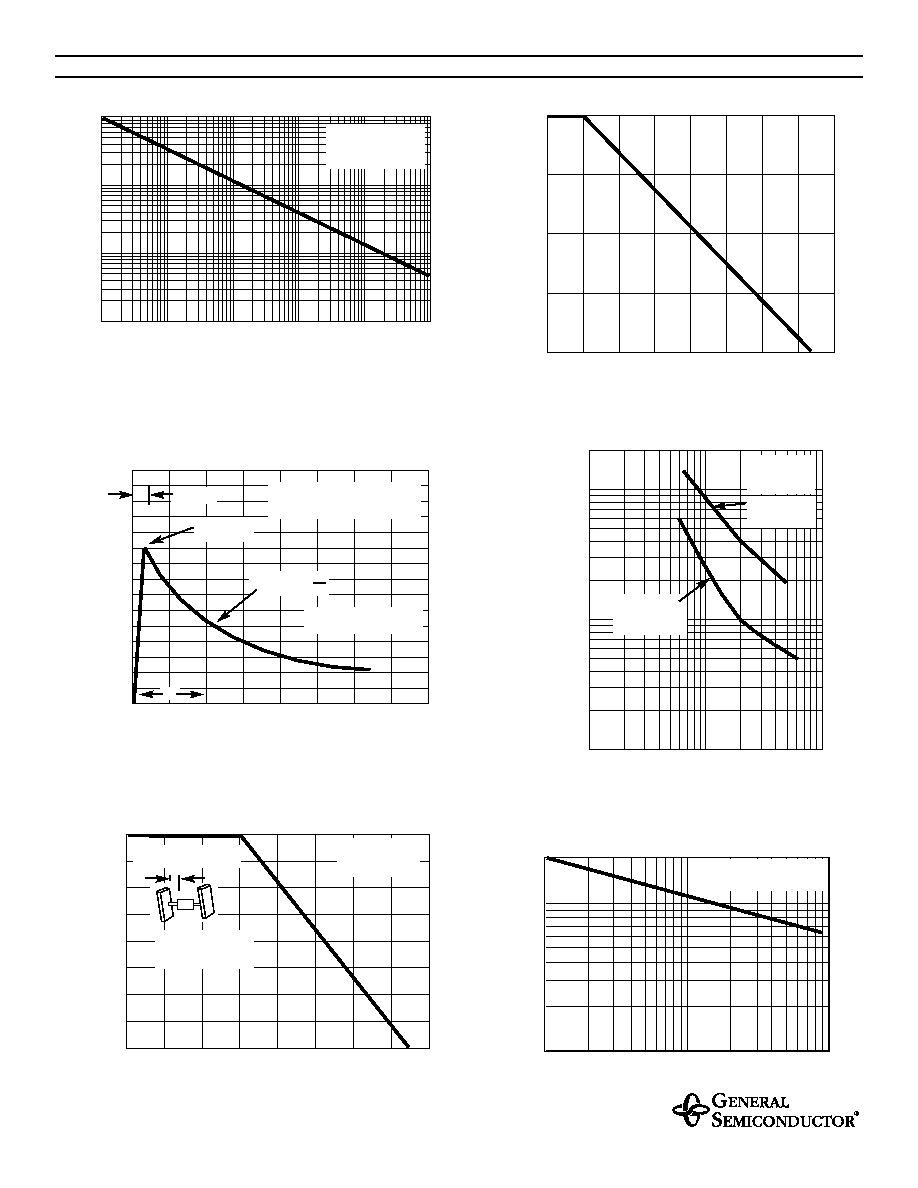
RATINGS AND CHARACTERISTIC CURVES 1.5KA6.8 THRU 1.5KA43A
FIG. 1 - PEAK PULSE POWER RATING CURVE
P
PPM
, PEAK PULSE POWER, kW
td, PULSE WIDTH, sec.
T
A
, AMBIENT TEMPERATURE, ∞C
FIG. 4 - TYPICAL JUNCTION CAPACITANCE
UNIDIRECTIONAL
FIG. 3 - PULSE WAVEFORM
t, TIME, ms
V
(BR)
, BREAKDOWN VOLTAGE, VOLTS
T
L,
LEAD TEMPERATURE,∞C
NUMBER OF CYCLES AT 60 H
Z
I
PPM
PEAK PULSE CURRENT
, %
PEAK PULSE POWER (P
PP
) or CURRENT
(I
PP
)
DERA
TING IN PERCENT
AGE, %
C
J
, CAP
ACIT
ANCE , pF
I
FSM,
PEAK FOR
W
ARD SURGE CURRENT
,
AMPERES
NON-REPETITIVE
PULSE WAVEFORM
SHOWN in FIG. 3
T
A
=25∞C
PULSE WIDTH (t
d
) is DEFINED
as the POINT WHERE the PEAK
CURRENT DECAYS to 50% of I
PP
t
r
=10
µ
sec.
T
J
=25∞C
f=1.0 MHZ
V
SIG
=50mV
P-P
MEASURED at
ZERO BIAS
MEASURED at
STAND-OFF
VOLTAGE, V
WM
0.8 x 0.8 x 0.040"
(20 x 20 x 1mm)
COPPER HEAT SINKS
60 H
Z
RESISTIVE OR
INDUCTIVE LOAD
T
L
=75∞C
8.3
ms
SINGLE HALF SINE-WAVE
(JEDEC Method)
td
HALF VALUE - I
PP
2
10/1000
µ
sec. WAVEFORM
as DEFINED by R.E.A.
FIG. 6 - MAXIMUM NON-REPETITIVE FORWARD
SURGE CURRENT
PEAK VALUE
I
PPM
FIG. 5 - STEADY STATE POWER DERATING
CURVE
PM
(A
V),
STEADY
ST
A
TE POWER DISSIP
A
TION,
W
A
TTS
FIG. 2 - PULSE DERATING CURVE
=0.375" (9.5mm)
LEAD LENGTHS
L