 | –≠–ª–µ–∫—Ç—Ä–æ–Ω–Ω—ã–π –∫–æ–º–ø–æ–Ω–µ–Ω—Ç: 2N3904 | –°–∫–∞—á–∞—Ç—å:  PDF PDF  ZIP ZIP |
2N3904
SMALL SIGNAL TRANSISTORS (NPN)
FEATURES
® NPN Silicon Epitaxial Planar Transistor for
switching and amplifier applications.
® As complementary type, the PNP transistor
2N3906 is recommended.
® On special request, this transistor is also
manufactured in the pin configuration
TO-18.
® This transistor is also available in the SOT-23 case
with the type designation MMBT3904.
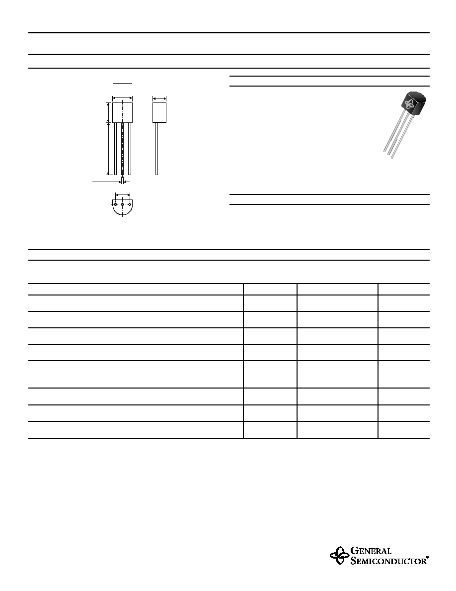
MECHANICAL DATA
Case: TO-92 Plastic Package
Weight: approx. 0.18g
MAXIMUM RATINGS AND ELECTRICAL CHARACTERISTICS
Ratings at 25°C ambient temperature unless otherwise specified
SYMBOL
VALUE
UNIT
Collector-Base Voltage
V
CBO
60
V
Collector-Emitter Voltage
V
CEO
40
V
Emitter-Base Voltage
V
EBO
6.0
V
Collector Current
I
C
200
mA
Power Dissipation at T
A
= 25°C
P
tot
625
mW
at T
C
= 25°C
1.5
W
Thermal Resistance Junction to Ambient Air
R
qJA
250
(1)
°C/W
Junction Temperature
T
j
150
°C
Storage Temperature Range
T
S
– 65 to +150
°C
NOTES:
(1) Valid provided that leads are kept at ambient temperature.
0.181 (4.6)
m
i
n
.
0.492
(12.5
)
0.1
81 (4
.6)
0.142 (3.6)
0.098 (2.5)
max.
∆ 0.022 (0.55)
E
C
B
TO-92
1/5/99
Dimensions in inches and (millimeters)
NEW PRODUCT
NEW PRODUCT
NEW PRODUCT
2N3904
ELECTRICAL CHARACTERISTICS
Ratings at 25°C ambient temperature unless otherwise specified
SYMBOL
MIN.
MAX.
UNIT
Collector-Base Breakdown Voltage
at I
C
= 10
mA, I
E
= 0
V
(BR)CBO
60
–
V
Collector-Emitter Breakdown Voltage
at I
C
= 1 mA, I
B
= 0
V
(BR)CEO
40
–
V
Emitter-Base Breakdown Voltage
at I
E
= 10
mA, I
C
= 0
V
(BR)EBO
6
–
V
Collector Saturation Voltage
at I
C
= 10 mA, I
B
= 1 mA
V
CEsat
–
0.2
V
at I
C
= 50 mA, I
B
= 5 mA
V
CEsat
–
0.3
V
Base Saturation Voltage
at I
C
= 10 mA, I
B
= 1 mA
V
BEsat
–
0.85
V
at I
C
= 50 mA, I
B
= 5 mA
V
BEsat
–
0.95
V
Collector-Emitter Cutoff Current
V
EB
= 3 V, V
CE
= 30 V
I
CEV
–
50
nA
Emitter-Base Cutoff Current
V
EB
= 3 V, V
CE
= 30 V
I
EBV
–
50
nA
DC Current Gain
at V
CE
= 1 V, I
C
= 0.1 mA
h
FE
40
–
–
at V
CE
= 1 V, I
C
= 1 mA
h
FE
70
–
–
at V
CE
= 1 V, I
C
= 10 mA
h
FE
100
300
–
at V
CE
= 1 V, I
C
= 50 mA
h
FE
60
–
–
at V
CE
= 1 V, I
C
= 100 mA
h
FE
30
–
–
Input Impedance
at V
CE
= 10 V, I
C
= 1 mA, f = 1 kHz
h
ie
1
10
k
W
Voltage Feedback Ratio
at V
CE
= 10 V, I
C
= 1 mA, f = 1 kHz
h
re
0.5 · 10
–4
8 · 10
–4
–
Gain-Bandwidth Product
at V
CE
= 20 V, I
C
= 10 mA, f = 100 MHz
f
T
300
–
MHz
Collector-Base Capacitance
at V
CB
= 5 V, f = 100 kHz
C
CBO
–
4
pF
Emitter-Base Capacitance
at V
EB
= 0.5 V, f = 100 kHz
C
EBO
–
8
pF
2N3904
ELECTRICAL CHARACTERISTICS
Ratings at 25°C ambient temperature unless otherwise specified
SYMBOL
MIN.
MAX.
UNIT
Small Signal Current Gain
at V
CE
= 10 V, I
C
= 1 mA, f = 1 kHz
h
fe
100
400
–
Output Admittance
at V
CE
= 1 V, I
C
= 1 mA, f = 1 kHz
h
oe
1
40
mS
Noise Figure
at V
CE
= 5 V, I
C
= 100
mA, R
G
= 1 k
W,
f = 10 … 15000 Hz
NF
–
5
dB
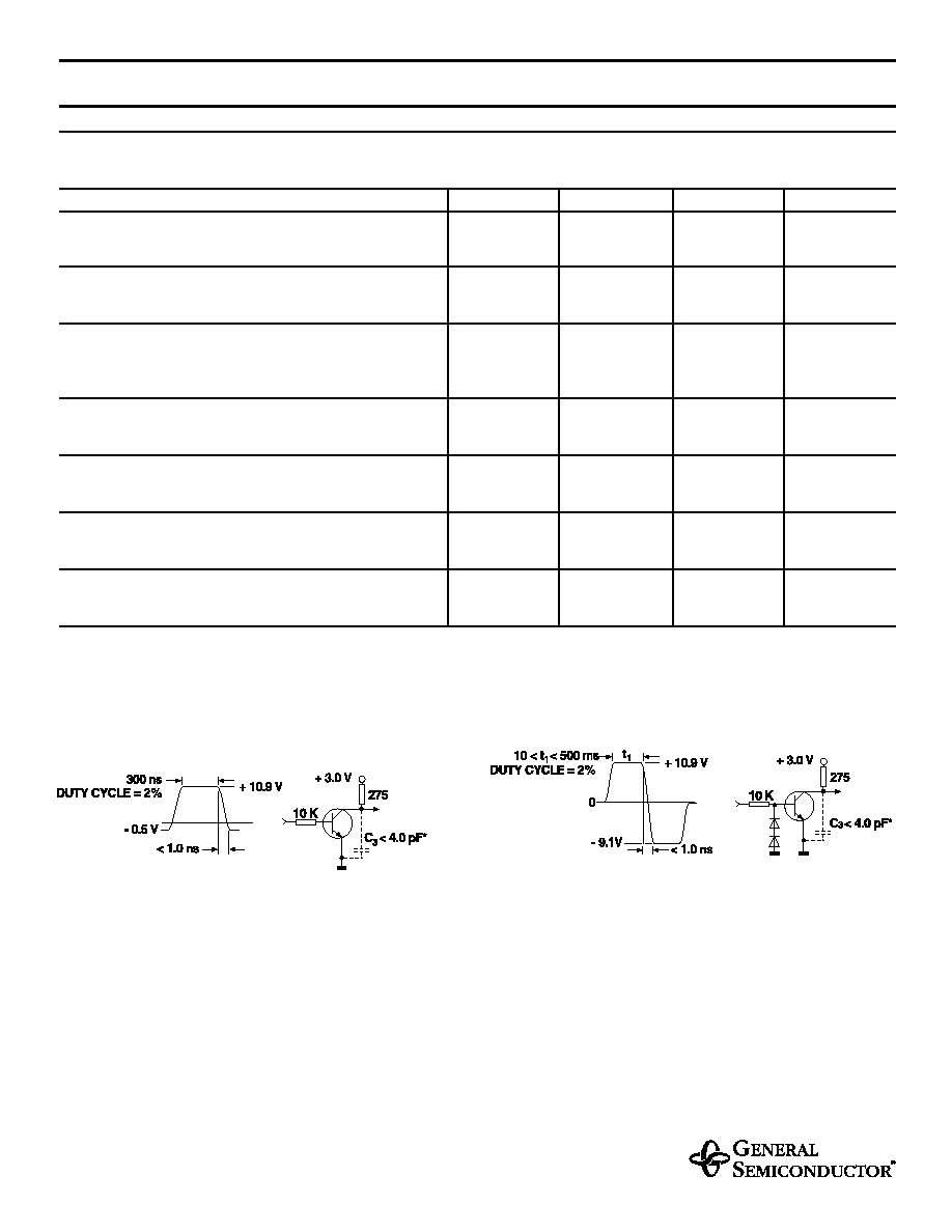
Delay Time (see Fig. 1)
at I
B1
= 1 mA, I
C
= 10 mA
t
d
–
35
ns
Rise Time (see Fig. 1)
at I
B1
= 1 mA, I
C
= 10 mA
t
r
–
35
ns
Storage Time (see Fig. 2)
at –I
B1
= I
B2
= 1 mA, I
C
= 10 mA
t
s
–
200
ns
Fall Time (see Fig. 2)
at –I
B1
= I
B2
= 1 mA, I
C
= 10 mA
t
f
–
50
ns
Fig. 2: Test circuit for storage and fall time
* total shunt capacitance of test jig and connectors
Fig. 1: Test circuit for delay and rise time
* total shunt capacitance of test jig and connectors