SMCG AND SMCJ5.0 THRU 170CA
SURFACE MOUNT T
RANS
Z
ORB
TM TRANSIENT VOLTAGE SUPPRESSOR
Stand-off Voltage - 5.0 - 170 Volts Peak Pulse Power - 1500 Watts
FEATURES
Plastic package has Underwriters
Laboratory Flammability Classification 94V-0
For surface mounted applications in order to optimize
board space
Low profile package
Built-in strain relief
Glass passivated junction
Low inductance
1500W peak pulse power capability with a 10/1000
µ
s
waveform, repetition rate (duty cycle): 0.01%
Excellent clamping capability
Fast response time: typically less than 1.0ps from 0 Volts
to V
(BR)
for uni-directional and 5.0ns for bi-directional types
For devices with V
(BR)
10V, I
D
are typically less
than 1.0
µ
A
High temperature soldering guaranteed:
250∞C/10 seconds at terminals
MECHANICAL DATA
Case: JEDEC DO214AB / DO215AB molded plastic over
passivated junction
Terminals: Solder plated, solderable per MIL-STD-750,
Method 2026
Polarity: For unidirectional types the color band denotes the
cathode, which is postitive with respect to the anode under
normal TVS operation
Mounting Position: Any
Weight: 0.007 ounces, 0.21 gram
DEVICES FOR BI-DIRECTIONAL APPLICATIONS
For bi-directional use add suffix C or CA for types SMC-5.0 thru SMC-170 (e.g. SMCG5.0C, SMCJ170CA).
Electrical characteristics apply in both directions.
MAXIMUM RATINGS AND ELECTRICAL CHARACTERISTICS
Ratings at 25∞C ambient temperature unless otherwise specified.
SYMBOLS
VALUE
UNITS
Peak pulse power dissipation with a 10/1000
µ
s waveform
(NOTES 1, 2, FIG. 1)
P
PPM
Minimum 1500
Watts
Peak pulse current with a 10/1000
µ
s waveform
(NOTE 1, FIG. 3)
I
PPM
SEE TABLE 1
Amps
Peak forward surge current 8.3ms single half sine-wave superimposed
on rated load (JEDEC Method)
(NOTES 2, 3)
- uni-directional only
I
FSM
200.0
Amps
Maximum instantaneous forward voltage at 100A
(NOTE 3)
uni-directional only
V
F
3.5
Volts
Operating junction and storage temperature range
T
J
, T
STG
-55 to +150
∞C
NOTES:
(1) Non-repetitive current pulse, per Fig.3 and derated above T
A
=25∞C per Fig. 2
(2) Mounted on 0.31 x 0.31" (8.0 x 8.0mm) copper pads to each terminal
(3) Measured on 8.3ms single half sine-wave. For uni-directional devices only.
Dimensions in inches and (millimeters)
DO-215AB
GULL WING
DO-214AB
MODIFIED J-BEND
0.280 (7.11)
0.260 (6.60)
0.016 (0.41)
0.006 (0.15)
0.020
(0.51)
MAX.
0.058 (1.47)
0.038 (0.97)
0.400 (10.16)
0.380 (9.64)
0.032 (8.10)
0.024 (6.10)
0.008 (0.20)
0.004 (0.10)
SEATING
PLANE
0.245 (6.22)
0.130 (5.72)
0.125 (3.17)
0.115 (2.92)
0.095 (2.41)
0.075 (1.90)
0.006 (0.152)
0.012 (0.305)
0.030 (0.76)
0.060 (1.52)
0.008 (0.203)
0.305 (7.75)
0.320 (8.13)
0.260 (6.60)
0.280 (7.11)
0.079 (2.06)
0.103 (2.62)
0.220 (5.59)
0.245 (6.22)
0.126 (3.20)
0.114 (2.90)
MAX.
1/25/99
ELECTRICAL CHARACTERISTICS at (T
A
=
25∞C unless otherwise noted) TABLE 1 (Cont'd)
Breakdown
Maximum
Maximum
Device
Voltage
Reverse
Peak Pulse
Maximum
Device Type
Device Type
Marking
V
(BR)
(Volts)
Test
Stand-off
Leakage
Surge
Clamping
Gull Wing
Modified
Code
(NOTE 1)
Current
Voltage
at V
WM
Current I
PPM
Voltage at I
PPM
Lead
"J" Bend Lead
UNI BI
(MIN / MAX)
at I
T
(mA)
V
WM
(Volts)
(NOTE 3)
I
D
(
µ
A)
(NOTE 2)
(Amps)
V
C
(Volts)
SMCG54
SMCJ54
GGD
60.0 / 73.3
1.0
54.0
5.0
15.6
96.3
SMCG54A
SMCJ54A
GGE
60.0 / 66.3
1.0
54.0
5.0
17.2
87.1
SMCG58
SMCJ58
GGF
64.4 / 78.7
1.0
58
5.0
14.6
103
SMCG58A
SMCJ58A
GGG
6.4.4 / 71.2
1.0
58
5.0
16.0
93
SMCG60
SMCJ60
GGH
66.7 / 81.5
1.0
60
5.0
14.0
107
SMCG60A
SMCJ60A
GGK
66.7 / 73.7
1.0
60
5.0
15.5
96
SMCG64
SMCJ64
GGL
71.1 / 86.9
1.0
64
5.0
13.2
114
SMCG64A
SMCJ64A
GGM
71.1 / 78.6
1.0
64
5.0
14.6
103
SMCG70
SMCJ70
GGN
77.8 / 95.1
1.0
70
5.0
12.0
125
SMCG70A
SMCJ70A
GGP
77.8 / 86.0
1.0
70
5.0
13.3
113
SMCG75
SMCJ75
GGQ
83.3 / 102
1.0
75
5.0
11.2
134
SMCG75A
SMCJ75A
GGR
83.3 / 92.1
1.0
75
5.0
12.4
121
SMCG78
SMCJ78
GGS
86.7 / 106
1.0
78
5.0
10.8
139
SMCG78A
SMCJ78A
GGT
86.7 / 95.8
1.0
78
5.0
11.9
126
SMCG85
SMCJ85
GGU
94.4 / 115
1.0
85
5.0
9.9
151
SMCG85A
SMCJ85A
GGV
94.4 / 104
1.0
85
5.0
10.9
137
SMCG90
SMCJ90
GGW
100 / 122
1.0
90
5.0
9.4
160
SMCG90A
SMCJ90A
GGX
100 / 111
1.0
90
5.0
10.3
146
SMCG100
SMCJ100
GGY
111 / 136
1.0
100
5.0
8.4
179
SMCG100A
SMCJ100A
GGZ
111 / 123
1.0
100
5.0
9.3
162
SMCG110
SMCJ110
GHD
122 / 149
1.0
110
5.0
7.7
196
SMCG110A
SMCJ110A
GHE
122 / 135
1.0
110
5.0
8.5
177
SMCG120
SMCJ120
GHF
133 / 163
1.0
120
5.0
7.0
214
SMCG120A
SMCJ120A
GHG
133 / 147
1.0
120
5.0
7.8
193
SMCG130
SMCJ130
GHH
144 / 176
1.0
130
5.0
6.5
231
SMCG130A
SMCJ130A
GHK
144 / 159
1.0
130
5.0
7.2
209
SMCG150
SMCJ150
GHL
16.7 / 204
1.0
150
5.0
5.6
268
SMCG150A
SMCJ150A
GHM
167 / 185
1.0
150
5.0
6.2
243
SMCG160
SMCJ160
GHN
178 / 218
1.0
160
5.0
5.2
287
SMCG160A
SMCJ160A
GHP
178 / 197
1.0
160
5.0
5.8
259
SMCG170
SMCJ170
GHQ
189 / 231
1.0
170
5.0
4.9
304
SMCG170A
SMCJ170A
GHR
189 / 209
1.0
170
5.0
5.5
275
N0TES:
(1) V
(BR)
measured after I
T
applied for 300
µ
s square wave pulse or equivalent
(2) Surge current waveform per Fig. 3 and derate per Fig. 2
(3) For bi-directional types having V
WM
of 10 Volts and less, the I
D
limit is doubled
(4) For the bi-directional SMCG/SMCJ5.0CA, the maximum V
(BR)
is 7.25 Volts
(5) All terms and symbols are consistent with ANSI/IEEE C62.35
APPLICATION N0TES
These surface mountable packages are designed specifically for transient voltage suppression. The wide leads assure a large sur-
face contact for good heat dissipation, and a low resistance path for surge current flow to ground. These high speed transient voltage
suppressors can be used to effectively protect sensitive components such as integrated circuits and MOS devices.
A 1500W (SMC) device is normally selected when the threat of transients is from lightning-induced transients conducted via external
leads or I/0 lines. It is also used to protect against switching transients induced by large coils or industrial motors.
System impedance at component level in a system is usually high enough to limit the current to within the peak pulse current (I
PP
)
rating of this series.
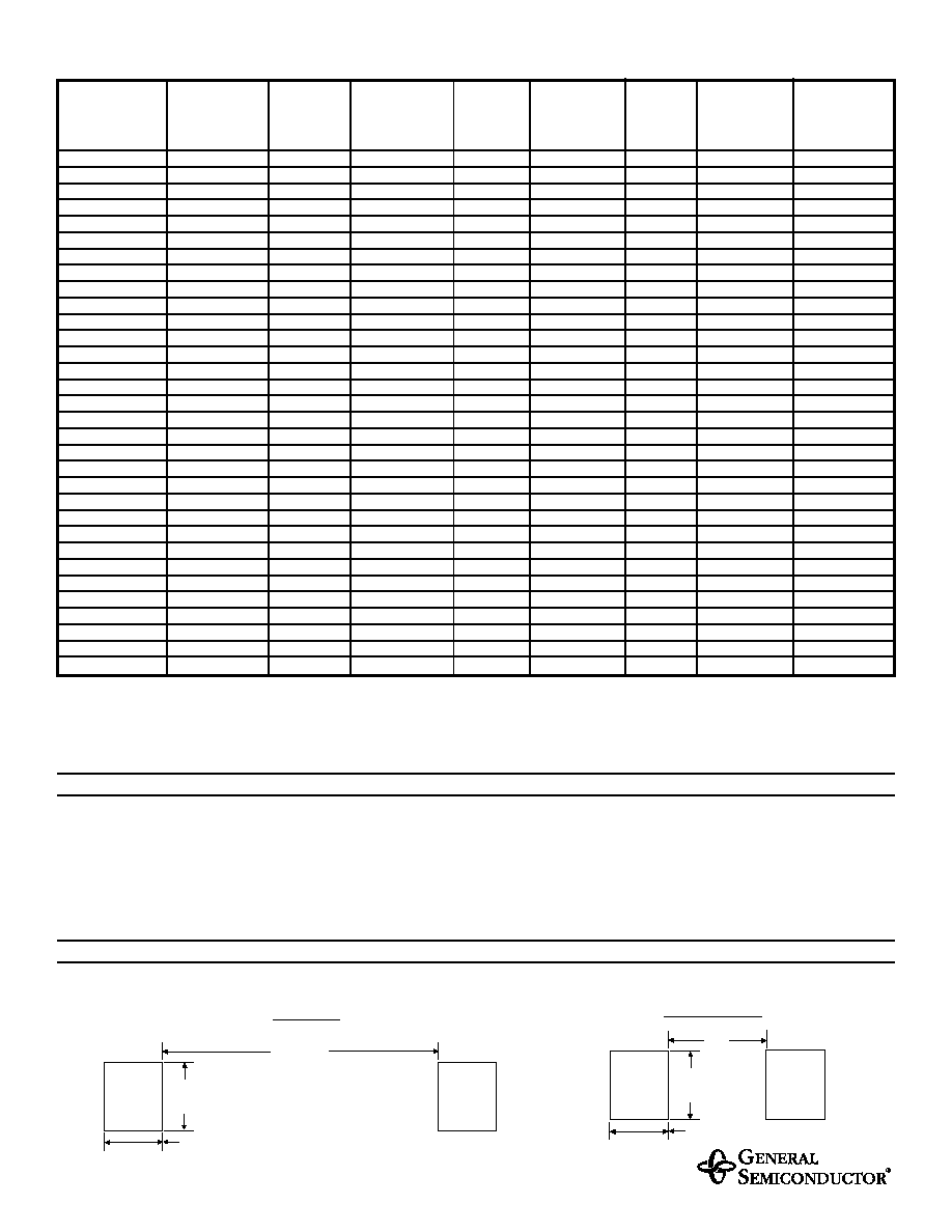
RECOMMENDED PAD SIZES
The pad dimensions should be 0.010" (0.25mm) longer than the contact size, in the lead axis.
This allows a solder fillet to form, see figure below. Contact factory for soldering methods.
0.310" (7.87)
0.125" (3.17)
0.050" (1.27)
0.190" (4.83)
0.125" (3.17)
0.070" (1.78)
MODIFIED J-BEND
GULL- WING
GGD
GGE
GGF
GGG
GGH
GGK
GGL
GGM
GGN
GGP
GGQ
GGR
GGS
GGT
GGU
GGV
GGW
GGX
GGY
GGZ
GHD
GHE
GHF
GHG
GHH
GHK
GHL
GHM
GHN
GHP
GHQ
GHR
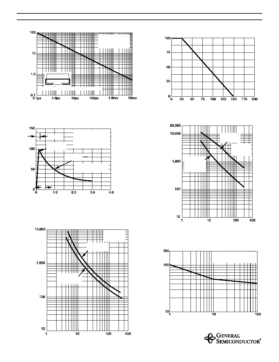
MAXIMUM RATINGS AND CHARACTERISTIC CURVES SMCG AND SMCJ5.0 THRU 170CA
FIG. 1 - PEAK PULSE POWER RATING CURVE
P
PPM
, PEAK PULSE POWER, kW
td, PULSE WIDTH, sec.
T
A
, AMBIENT TEMPERATURE, ∞C
FIG. 4 - TYPICAL JUNCTION CAPACITANCE
UNI-DIRECTIONAL
FIG. 3 - PULSE WAVEFORM
t, TIME, ms
V
WM
, REVERSE STAND-OFF VOLTAGE,
VOLTS
V
WM,
STAND-OFF VOLTAGE, VOLTS
NUMBER OF CYCLES AT 60 H
Z
I
PPM
PEAK PULSE CURRENT
, % I
RSM
PEAK PULSE POWER (P
PP
) or CURRENT
(I
PP
)
DERA
TING IN PERCENT
AGE, %
C
J
, CAP
ACIT
ANCE, pF
C
J
, JUNCTION CAP
ACIT
ANCE, pF
I
FSM
, PEAK FOR
W
ARD SURGE CURRENT
,
AMPERES
NON-REPETITIVE
PULSE WAVEFORM
SHOWN in FIG. 3
T
A
=25∞C
T
J
=25∞C PULSE WIDTH (td)
is DEFINED as the POINT
WHERE the PEAK
CURRENT DECAYS
to 50% of I
PPM
tr=10
µ
sec.
MEASURED at
ZERO BIAS
V
R,
MEASURED
at STAND-OFF
VOLTAGE, V
WM
8.3ms SINGLE HALF SINE-WAVE
(JEDEC Method)
UNIDIRECTIONAL ONLY
HALF VALUE - I
PP
2
10/1000
µ
sec. WAVEFORM
as DEFINED by R.E.A.
FIG. 6 - MAXIMUM NON-REPETITIVE PEAK FORWARD
SURGE CURRENT
PEAK VALUE
I
PPM
FIG. 5 - TYPICAL JUNCTION CAPACITANCE
BI-DIRECTIONAL
FIG. 2 - PULSE DERATING CURVE
T
J
=25∞C
f=1.0 MH
Z
Vsig=50mVp-p
T
J
=25∞C
f=1.0 MH
Z
Vsig=50mVp-p
0.31 X 0.31" (8.0 X 8.0mm) COPPER PAD AREAS
MEASURED at
ZERO BIAS
MEASURED at
STAND-OFF
VOLTAGE, V
WM
td