 | –≠–ª–µ–∫—Ç—Ä–æ–Ω–Ω—ã–π –∫–æ–º–ø–æ–Ω–µ–Ω—Ç: GB4551 | –°–∫–∞—á–∞—Ç—å:  PDF PDF  ZIP ZIP |
FEATURES
∑
accurate clamping to within
±
1mV
∑
ultra low differential gain (0.03% typ.)
and differential phase (0.03
o
typ.)
∑
wideband unity gain, can typically be flattened to
±
0.1dB at 30MHz
∑
can be configured as a gain stage with reduced
bandwidth.
∑
drives 100pF loads
∑
convenient 8 pin SIP packaging
Pin No.
GB4551
Function
1
+IN
non-inverting input
2
V
CC
positive power supply
3
STB
strobe
4
GND
ground
5
C
X
external capacitor
6
V
EE
negative power supply
7
- IN
inverting input
8
OUT
output
ORDERING INFORMATION
Part Number Package Type Temperature Range
GB4551-CSA 8 Pin SIP
0 to 70
o
C
GENNUM CORPORATION P.O. Box 489, Stn A, Burlington, Ontario, Canada L7R 3Y3 tel. (905) 632-2996 fax: (905) 632-2055
Japan Branch: B-201 Miyamae Village, 2-10-42 Miyamae, Suginami-ku Tokyo 168, Japan tel. (03) 3247-8838 fax: (03) 3247-8839
DATA SHEET
GB4551 Video Buffer with
Strobed DC Restore
Document No. 520 - 52 - 2
DESCRIPTION
The GB4551 is a high performance video buffer with DC
restore primarily used for accurate back porch clamping.
The circuit features a wideband differential amplifier that
can be configured as a gain stage. The output signal
voltage is limited to +2V above the clamp level in order to
prevent damage to crosspoints or other circuits connected
to the output.
The clamping action occurs when the STROBE (STB)
input is taken to ground. A typical application would be for
DC restoration during the back porch period. In this case
the negative-going back porch pulse would be derived
from an external sync separator circuit.
The GB4551 will operate from
±
9V to
±
12V power supplies
and will directly interface with Gennum's video crosspoint
switches. The 8 pin SIP package is ideally suited for
space restricted board layouts.
APPLICATIONS
∑ Input buffering and DC restoration to crosspoint switches
∑ Accurate back porch video signal clamping
∑ Inter-circuit buffering and DC restoration.
V
CC
500
10k
≠IN
OUT
C
X
30k
+IN
V
EE
STROBE
12pF
10k
GND
(+2V OUTPUT CLAMP)
7mA
NOM.
+
-
+
-
SIMPLIFIED CIRCUIT DIAGRAM
All resistors in ohms, all capacitors in microfarads unless otherwise stated.
PIN CONNECTIONS
1 2 3 4 5 6 7 8
GB4551

2
520 - 52 - 2
PARAMETER
SYMBOL
CONDITIONS
MIN
TYP
MAX
UNITS
Supply Voltage
V
S
Operating Range
±
9
±
10
±
12
V
+ Supply Current
I
+
-
9
13.8
mA
≠ Supply Current
I-
-
9
13.8
mA
Frequency Response
at
±
0.1dB (NOTE 1, see Fig. 5)
25
-
-
MHz
Full Power Bandwidth
FPBW
at -3dB V
IN
= 1V p-p
30
-
-
MHz
Phase Delay
at 3.58MHz (see Fig. 4)
-
-3.0
-
deg
Phase Variation
at 3.58MHz
-
±
0.1
±
0.2
deg
Differential Gain
g
at 3.58MHz (V
IN
= 40 IRE)
-
0.03
0.05
%
Differential Phase
p
at 3.58MHz (V
IN
= 40 IRE)
-
0.03
0.05
degrees
Max. Input Voltage
V
IN(MAX)
A
V
=+1 Clipping occurs at:
1.8
2.0
2.2
V
Input Resistance
R
IN
25
30
-
k
Input Capacitance
C
IN
A
V
=+1
-
2.0
-
pF
Output Resistance
R
OUT
A
V
=+1, = 0 to1MHz
-
8.6
-
A
V
=+1, = 100MHz
-
53
-
Clamp Accuracy
V
IN
=+1V p-p
-
±
1
±
2
mV
Strobe Pulse Width
t
P STROBE
500
1000
-
ns
Strobe Level
V
INHI
2.0
-
-
V
V
INLO
-
-
0.8
V
POWER
SUPPLIES
SIGNAL
PATH
STROBE
ABSOLUTE MAXIMUM RATINGS
PARAMETER
VALUE/UNITS
Supply Voltage
±
13.5 V
Operating Temperature Range
0
∞
C
T
A
70
∞
C
Storage Temperature Range
-65
∞
C
T
S
150
∞
C
Lead Temperature (Soldering, 10 sec)
260
∞
C
Differential Video Input Voltage
±
5 V
Strobe Input Voltage
-V
s
V
STROBE
+V
s
V
S
=
±
10V, T
A
= 0
∞
C to 70
∞
C, R
L
= 10k
, C
L
= 10pF, unless otherwise shown
ELECTRICAL CHARACTERISTICS
CAUTION
CLASS 1 ESD SENSITIVITY
Note: 1.
The frequency peaking can be flattened by placing a small value series resistor at the GB4551 output. The value of the
resistor will depend on the load capacitance and the amount of flattening required. Figure 5 shows the frequency response
for three combinations of R
S
and C
L.

3
520 - 52 - 2
680k
-
10V
10
NON-POLAR
470p
+10V
GB4551
4 2 6
5 3 7
1 8
COMPOSITE
VIDEO INPUT
COLOR BURST
FILTER
0.1
6
4
8
5
2
CLAMPED
VIDEO OUTPUT
BACK
PORCH
PULSE
10V
0V
+10V
0.1
0.1
0.1
0.1
GS4881
SYNC. SEP.
Fig.1 Clamping Operation
DETAILED DESCRIPTION
The GB4551 is intended for video applications requiring
precision DC restoration coupled with very flat frequency
response. The signal path features a wide band operational
amplifier designed to be unity gain stable. While this amplifier
is not intended to drive 75
transmission lines, it is ideal for
applications where high capacitive loads, up to several
hundred picofarads, must be driven. These applications
include input and internal system buffering and DC restoration
of video signals.
Optimal frequency response for the GB4551 occurs with load
capacitances in the range of 80 pF. For smaller loads, an
external capacitor can be added to extend the bandwidth of
the device. As shown in Figure 7, a small resistor, R
OUT
,
should be included in series with the GB4551 output to obtain
optimal response flatness. The value of this resistor should be
chosen to match the value of the load capacitance, as shown
in Figure 5.
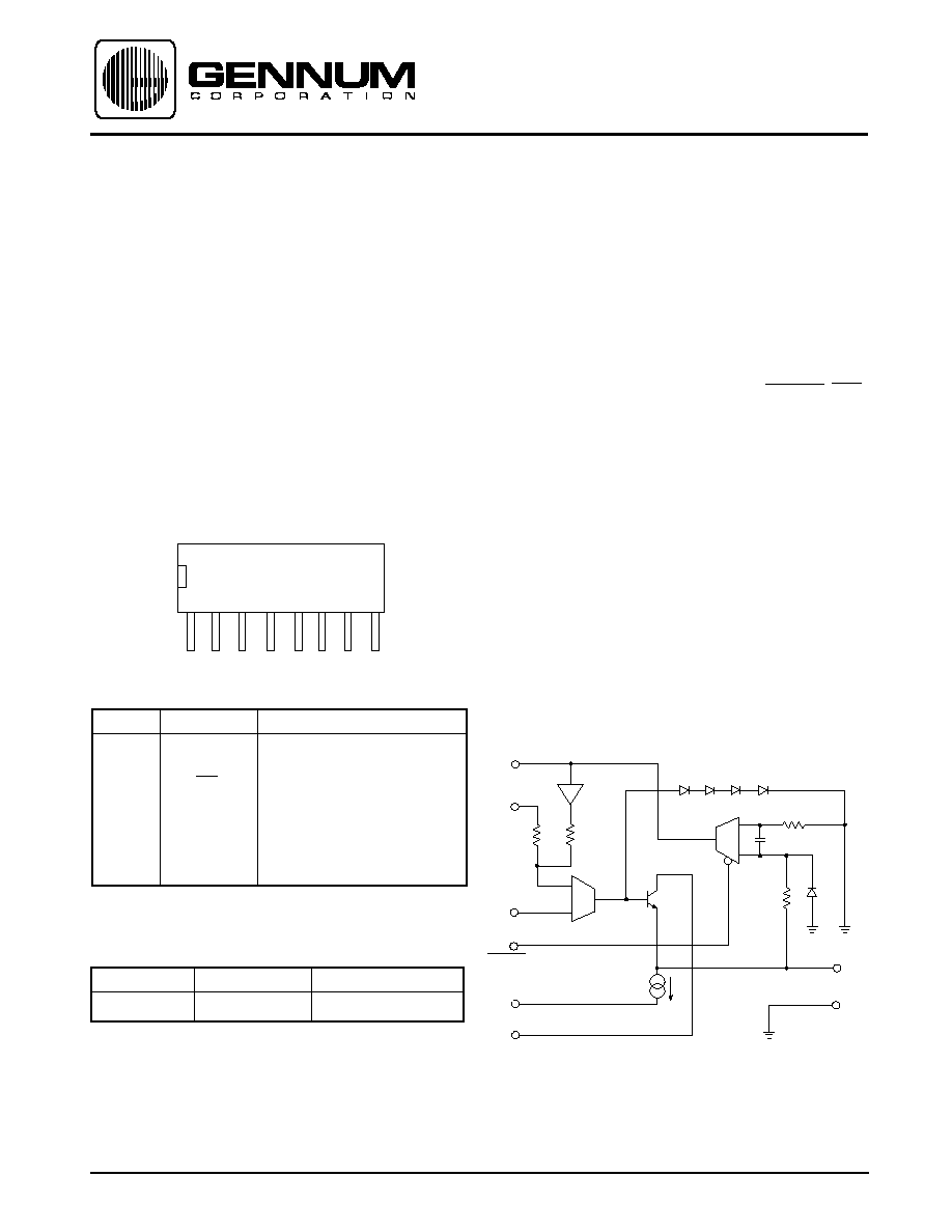
The DC restoration function is achieved through the use of a
strobed operational transconductance amplifier (OTA), as
shown in the Simplified Block Diagram. When enabled by
taking STROBE low, the OTA sources or sinks a current
depending on whether the output of the GB4551 is below or
above ground, respectively. The output current from the OTA
is integrated by the hold capacitor connected to pin 5, CX.
The resulting voltage is buffered and fed to the non-inverting
input of the op-amp through a 30 k
resistor. The non-inverting
input also receives the input video signal through a large
capacitor which acts as the DC reservoir for the corrective
level shift.
A 500
resistor in series with the input provides some phase
advance to improve the stability of the DC restoration feedback
loop, and provides fast recovery for offset steps as large as
±
100 mV (
±
14 IRE). The values of the input and hold capacitors
can be reduced to speed up the offset recovery time. The ratio
of the capacitors should be maintained at approximately
20,000:1 to ensure closed loop stability.
The OTA receives its inputs from a differential low pass filter.
This filter has a corner frequency of 600 kHz which attenuates
the color burst and any high frequency noise that may be
present in the signal. One input to the low pass filter senses the
output of the GB4551 while the other input is connected to the
ground reference.
In the application shown in figure 1, the input to pin 3 of the
GB4551, STROBE, is provided by the back porch output of the
GS4881 sync separator. The GS4881 generates back porch
pulses which remain at horizontal rate throughout the vertical
interval. Constant rate sample pulses eliminate the possibility
of introducing additional DC offset due to a change in duty
cycle.
The method of adjusting the DC level of the video signal used
in the GB4551 integrates over the entire back porch period.
This reduces sensitivity to noise and improves the accuracy of
the DC restoration compared with systems using sample and
hold techniques. Typical clamping accuracy of
±
1 mV is
achieved by the GB4551.
TEST CIRCUITS
All resistors in ohms, all capacitors
in microfarads unless otherwise stated.

4
520 - 52 - 2
10k
-
10V
10
VIDEO OUTPUT
TO NETWORK
ANALYSER I/P
470p
+10V
75
0.1
GB4551
4 2 6
5 3 7
1 8
+5V
C
L
NETWORK
ANALYSER
Sweep: 1-100MHz
Level: 0dBM
0.1
+5V
+5V
4
1
8
5
0.1
0.1
CLC110
R
S
GAIN (dB)
1
10
100
FREQUENCY (MHz)
Fig. 3 Gain vs Frequency
Fig. 4 Phase vs Frequency
PHASE(
o
)
FREQUENCY (MHz)
1 3 5 10
C
L
= 10pF
C
L
= 100pF
27pF
47pF
6
5
4
3
2
1
0
-1
-2
-3
-4
10pF
0.0
-0.5
-1.0
-1.5
-2.0
-2.5
-3.0
-3.5
-4.0
-4.5
-5.0
C
L
= 100pF
TYPICAL PERFORMANCE CURVES
(Unless otherwise shown V
S
=
±
10V)
0.050
0.045
0.040
0.035
0.030
0.025
0.020
0.015
0.010
0.005
0.0000
1
10
Fig. 5 Flattened Frequency Response
1
10
50
FREQUENCY (MHz)
GAIN (dB)
Fig. 6 Differential Gain & Phase vs Frequency
1
3
5
10
FREQUENCY (MHz)
dg
dp
33
/68pF
27
/120pF
18
/270pF
0.3
0.2
0.1
0.0
-0.1
-0.2
-0 .3
-0.4
-0.5
-0.6
-0.7
dg (%), dp (
∞
)
V
IN
= 40IRE
R
S
/ C
L
V
IN
= 100mVp-p
V
IN
= 100mVp-p
R
S
= 0
All resistors in ohms, all capacitors
in microfarads unless otherwise stated.
Fig. 2 Differential Gain and Phase, Frequency Response

5
520 - 52 - 2
Gennum Corporation assumes no responsibility for the use of any circuits described herein and makes no representations that they are free from patent infringement.
© Copyright June 1992 Gennum Corporation. All rights reserved. Printed in Canada.
DOCUMENT
IDENTIFICATION
PRODUCT PROPOSAL
This data has been compiled for market investigation purposes
only, and does not constitute an offer for sale.
ADVANCE INFORMATION NOTE
This product is in development phase and specifications are
subject to change without notice. Gennum reserves the right to
remove the product at any time. Listing the product does not
constitute an offer for sale.
PRELIMINARY DATA SHEET
The product is in a preproduction phase and specifications are
subject to change without notice.
DATA SHEET
The product is in production. Gennum reserves the right to make
changes at any time to improve reliability, function or design, in
order to provide the best product possible.
The above circuit represents a possible use of the GB4551 as
an input back-porch clamp for video mixers in a simple
Production Switcher. For simplicity, the STROBE input is
derived from the GS4881 sync separator IC, driven from the
composite input signal.
The value of R
OUT
is chosen to roll-off the frequency response
of the GB4551. The value is usually between 15 and 47 ohms
depending on the total load capacitance seen by the device.
The GB4551 may be used anywhere in the circuit where
accurate DC restoration is required as shown by the second IC
following the output of the top GT4123.
COMPOSITE
VIDEO INPUT
COLOR BURST
FILTER
680k
-
10V
10
NON-POLAR
470p
+10V
GB4551
4 2 6
5 3 7
1 8
COMPOSITE
VIDEO INPUT
R
OUT
VID B
VID A
CONTROL
OUT
0.1
6
4
8
5
2
STROBE
TO OTHER
GB4551s
BORDER
INPUT FROM
(GB4551)
OUT
VID B
VID A
CONTROL
BACKGROUND
VIDEO IN
(FROM GB4551)
KEY INPUT
VID B
VID A
CONTROL
INSERT
GB4551
STROBE
VIDEO
OUTPUT 1
VIDEO
OUTPUT 2
BACK
PORCH
PULSE
5V
0V
3
5
1
7
3
5
1
7
3
5
1
7
GT4123
GT4123
GT4123
+5V
0.1
0.1
0.1
0.1
GS4881
SYNC. SEP.
APPLICATION CIRCUIT
Fig. 7 GB4551 Driving Several GT4123 Video Mixers
All resistors in ohms, all capacitors
in microfarads unless otherwise stated.