 | –≠–ª–µ–∫—Ç—Ä–æ–Ω–Ω—ã–π –∫–æ–º–ø–æ–Ω–µ–Ω—Ç: GB512 | –°–∫–∞—á–∞—Ç—å:  PDF PDF  ZIP ZIP |

∑ 8 pin PLID
∑ 8 pin SLT (LD512)
∑ Chip (61 x 61 mils)
Au Bump
DESCRIPTION
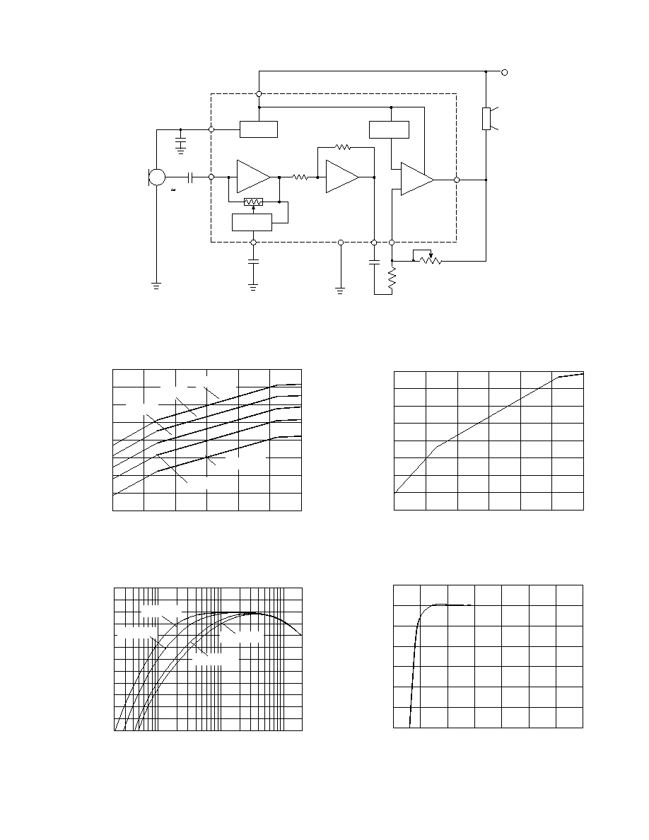
The GB512 and LD512 are 8 pin stand-alone input compression
amplifiers requiring minimal external parts. Each consists of a
voltage regulator for the electret microphone providing a high
power supply rejection ratio (PSRR), a compression stage
which has a 2:1 compression ratio, and an auto-biasing,
class A, voltage drive output stage.
The auto-bias output stage can drive a variety of impedances
ranging from 500
to 5 k
without adding any external
resistors to set the bias.
The GB512 and LD512 are recommended for low to medium
gain/output ITE and ITC type hearing aids.
The GB512 is tested to tighter test limits.
GB512/LD512 DATA SHEET
Low Parts
Compression Amplifier
FEATURES
∑ 44 dB typical preamplifier gain
∑ 14 dB typical output stage gain
∑ compression function ratio 1:1 to 2:1 to
:1
∑ automatic setting of transducer current
∑ operation down to 1.1 VDC
∑ greater than 40 dB volume control range
STANDARD PACKAGING
Document No. 500 - 75 - 08
200 mV
REF
V
REG
7
A IN
V
REG
C
AGC
3
8
4
5
6
1
C
+
_
B
-
-
A
GND B OUT C IN
C OUT
28 dB
16 dB
V
B
CONTROL
2
BLOCK DIAGRAM
Revision Date: January 2001
GENNUM CORPORATION P.O. Box 489, Stn A, Burlington, Ontario, Canada L7R 3Y3 tel. (905) 632-2996 fax: (905) 632-5946
Japan Branch: A-302, Miyamae Village, 2-10-42, Miyamae, Suginami-ku, Tokyo 168, Japan tel. (03) 3334-7700 fax (03) 3247-8839

2
500 - 75 - 08
1
4
5
8
A IN
V
B
GND
C OUT
C IN
PIN CONNECTION
ABSOLUTE MAXIMUM RATINGS
PARAMETER
VALUE/UNITS
Supply Voltage
5 V DC
Power Dissipation
25mW
Operating Temperature Range
-10
∞
C to 40
∞
C
Storage Temperature Range -20∞C to 70∞C
V
REG
C
AGC
B OUT
V
O
4
V
O
3
V
O
2
V
O
1
-40 dBV
IN
-54 dBV
IN
-74 dBV
IN
-88 dBV
IN
O/P
LEVEL
(dBV)
at PIN 1
Notes:
1.
V
O
and Distortion measurements are taken
at pin 1.
2.
Output stage gain = 20 log (R
F
/ R
S
).
A gain of 14 dB is recommended for
optimal stability. Stability is dependent
upon the ratio of the receiver impedance
(Z
L
) and the battery impedance to R
F
& R
S
.
(R
F
/ R
S
) < (Z
L
/
R
B
)
3.
V
BIAS
= V
P5
- V
P7
4.
Measured at pin 7
CAUTION
CLASS 1 ESD SENSITIVITY
290
0.98
-41
V
O1
+ 11
V
O2
+12
-18
3
4
300
-
-
-
110
0.88
-48
-
V
O2
+ 7
-23.5
-
-
160
3
-
-
200
0.93
-44
-
V
O2
+10
-20
1
2
200
8
100
5
290
0.98
-40
-
V
O2
+13
-17.5
3
4
240
-
-
-
µ
A
V
DC
dBV
dB
dB
dBV
µ
V
RMS
%
mVDC
mA
ms/
µ
F
ms/
µ
F
ELECTRICAL CHARACTERISTICS
Conditions : Temperature 25∞C, Frequency 1 kHz, Supply Voltage 1.3 VDC.
PARAMETER SYMBOL CONDITIONS MIN TYP MAX MIN TYP MAX UNITS
Amplifier Current
I
AMP
Regulator Voltage
V
REG
Output Level
V
O1
V
IN
= -88 dBV
Output Level
V
O2
V
IN
= -74 dBV
Output Level
V
O3
V
IN
= -54 dBV
Output Level
V
O4
V
IN
= -40 dBV
Input Referred Noise
IRN
NFB 0.2-10kHz at 12dB/oct
Total Harmonic Distortion
THD
V
IN
= -54 dBV
Receiver Bias Voltage
V
BIAS
Note 3
Current Sinking Capability
I
SINK
Note 4
Release Time Factor
T
REL
Attack Time Factor
T
ATT
200
0.93
-44
V
O1
+ 9
V
O2
+10
-20
1
2
200
8
100
5
110
0.88
-47
V
O1
+ 7
V
O2
+ 8
-23
-
-
100
3
-
-
GB512 LD512
All parameters and switches remain as shown in the Test Circuit unless stated in CONDITIONS column.
V
PX
- actual voltage measured on the pin at given condition (X is pin number).
3
500 - 75 - 08
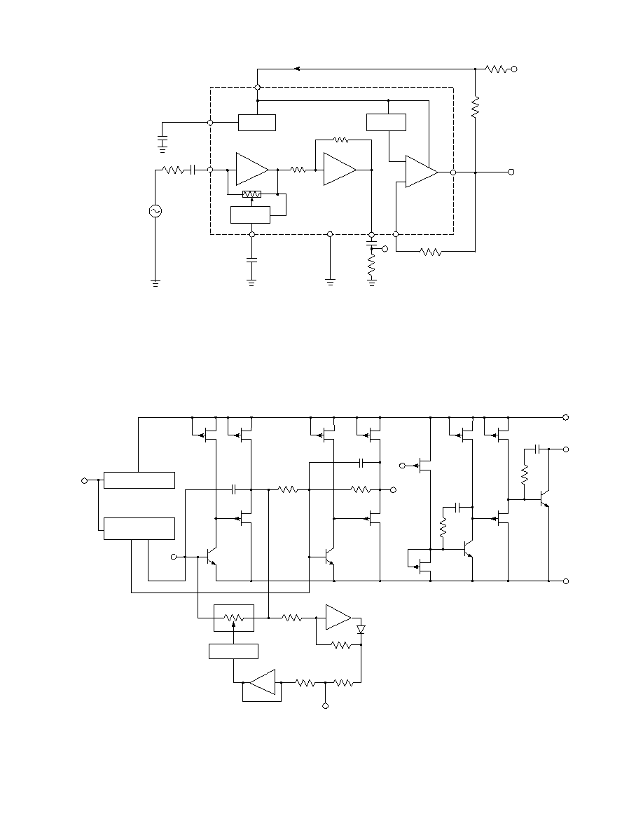
Fig. 2 Functional Schematic
REGULATOR
CONTROL
_
_
5
7
6
8
1
2
3
4
BASE CURRENT
COMPENSATION
120k
1k
Fig. 1 Test Circuit
I
AMP
V
O
22k
1µ0
V
IN
200 mV
REF
V
REG
7
2
3k9
0µ1
3
8
4
5
6
1
B
-
-
A
100k
0µ1
R
F
2k2
C
+
_
28 dB
16 dB
CONTROL
R
B
4
7
V
B
= 1.3 V
DC
1µ0
All resistors in ohms, all capacitors
in farads unless otherwise stated
4
500 - 75 - 08
V
B
=1.3 V
DC
1µ0
0µ1
ED1913
100k
R
VC
20K
1µ0
200 mV
REF
V
REG
7
3
8
4
5
6
1
C
+
_
B
-
-
A
28 dB
16 dB
CONTROL
2
R
S
3k9
0µ1
C
S
4
2
0
-2
-4
-6
-8
-10
-12
-14
-16
-18
-20
-100
-90
-80
-70
-60
-50
-40
-100
-90
-80
-70
-60
-50
-40
20 200 2K
20K
5
0
-5
-10
-15
-20
-25
-30
0.7 0.8 0.9 1.0 1.1 1.2 1.3 1.4
INPUT (dBV)
INPUT (dBV)
SUPPLY VOLTAGE (VDC)
RELATIVE GAIN (dB)
OUTPUT (dBV)
OUTPUT (dBV)
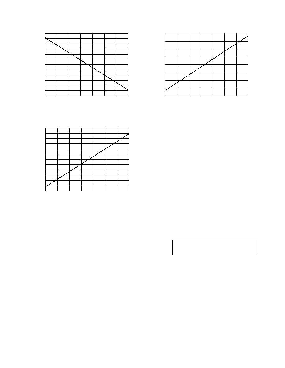
Fig. 4 I/O Characteristics at Various
R
VC
Values (Pin 7)
Fig. 5 I/O Characteristics at Pin 1
Fig. 7 Gain vs Supply Voltage
Fig. 6 Closed Loop Frequency Response
at Various C
S
Values
FREQUENCY
C
S
= 0.22
µ
F
C
S
= 0.1
µ
F
C
S
= 0.033
µ
F
C
S
= 0.047
µ
F
R
VC
= 100k
R
VC
= 47k
R
VC
= 22k
R
VC
= 3.3K
R
VC
= 10K
RELATIVE OUTPUT (dB)
All resistors in ohms, all capacitors
in farads unless otherwise stated
Fig. 3 Typical Hearing Aid Application
0
-10
-20
-30
-40
-50
-60
-70
-80
0
-10
-20
-30
-40
-50
-60
-70
-80
5
500 - 75 - 08
DOCUMENT
IDENTIFICATION
PRODUCT PROPOSAL
This data has been compiled for market investigation purposes
only, and does not constitute an offer for sale.
ADVANCE INFORMATION NOTE
This product is in development phase and specifications are
subject to change without notice. Gennum reserves the right to
remove the product at any time. Listing the product does not
constitute an offer for sale.
PRELIMINARY DATA SHEET
The product is in a preproduction phase and specifications are
subject to change without notice.
DATA SHEET
The product is in production. Gennum reserves the right to make
changes at any time to improve reliability, function or design, in
order to provide the best product possible.
Gennum Corporation assumes no responsibility for the use of any circuits described herein and makes no representations that they are free from patent infringement.
© Copyright Sept. 1982 Gennum Corporation. All rights reserved. Printed in Canada.
1.4
1.2
1.0
0.8
0.6
0.4
0.2
0.0
-0.2
-0.4
-0.6
-0.8
-1.0
30
20
10
0
-10
-20
-30
-40
-50
-20 -10 0 10 20 30 40 50
-20
-10 0 10 20 30 40 50
TEMPERATURE (∞C)
TEMPERATURE (∞C)
Fig. 9 Receiver Bias Voltage vs Temperature
Fig. 8 Gain vs Temperature
RELATIVE REFERENCE VOLTAGE (mV
DC
)
RELATIVE GAIN (dB)
-20 -10 0 10 20 30 40 50
50
40
30
20
10
0
-10
-20
-30
-40
-50
-60
-70
TEMPERATURE (∞C)
RELATIVE AMPLIFIER CURRENT (
µ
A)
Fig. 10 Amplifier Current vs Temperature
REVISION NOTES
Changes to standard packaging information.