 | –≠–ª–µ–∫—Ç—Ä–æ–Ω–Ω—ã–π –∫–æ–º–ø–æ–Ω–µ–Ω—Ç: GK509 | –°–∫–∞—á–∞—Ç—å:  PDF PDF  ZIP ZIP |

- A
MPO
A IN
R
V
E
B
GND
A OUT
R
MIC
VMIC
1
2
4
3
5
7
6
- B
B OUT
8
21K
R
E
GK509 DATA SHEET
Class A Amplifier with 2 DC Coupled
Gain Blocks & Schottky Diodes
FEATURES
∑
100
µ
A typical current drain
∑
low noise and distortion
∑
1.0 to 5 VDC operating range
∑
DC coupled stages
∑
Class A output stage
∑
Schottky diodes for MPO control
∑
variable transducer current
∑
4 k
microphone decoupling resistor
∑ 8 pin PLID
Æ
∑ Chip ( 61 x 55 mils)
STANDARD PACKAGING
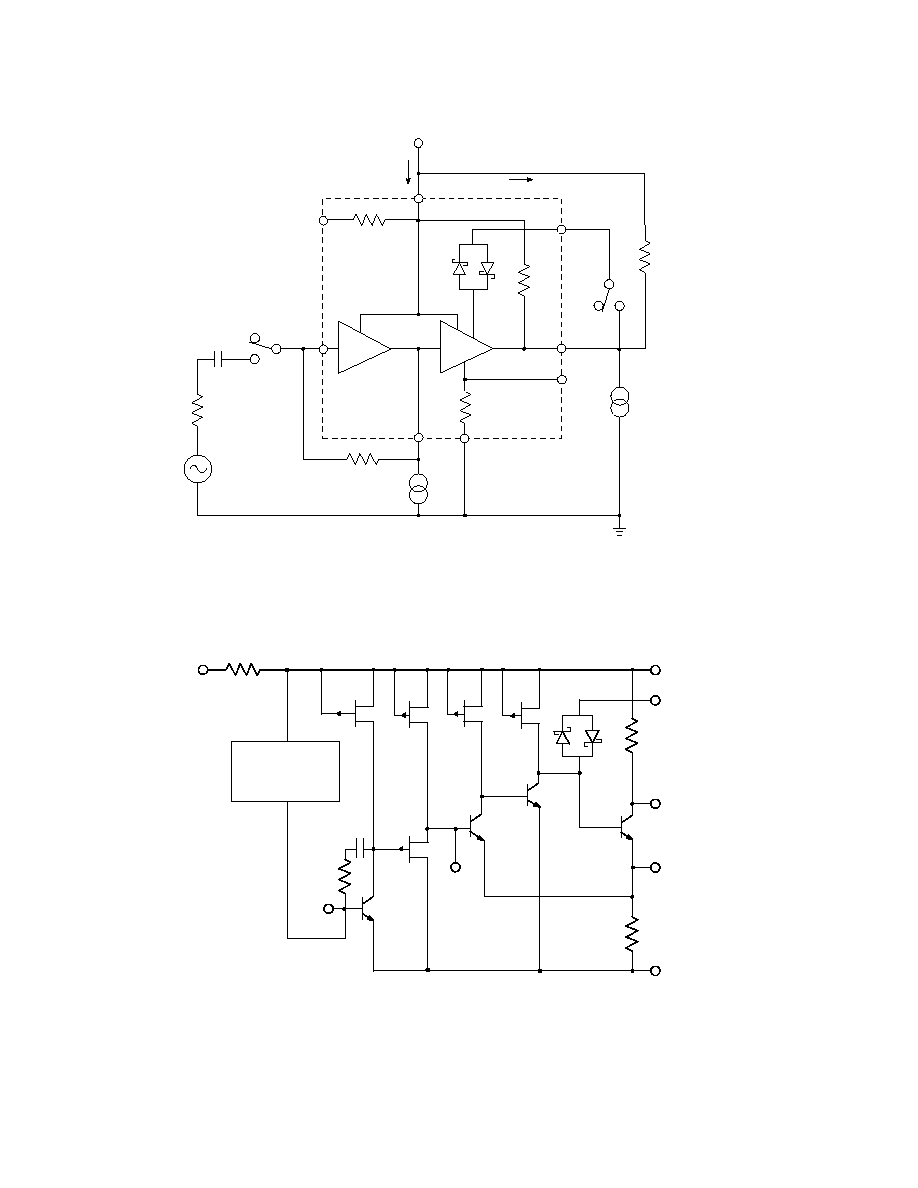
BLOCK DIAGRAM
All resistors in ohms, all capacitors in farads unless otherwise stated
DESCRIPTION
The GK509 is a Class A amplifier utilizing Gennum's
proprietary low voltage JFET technology. It consists of a
single-ended, low noise inverting gain block, a Class
A output s t a g e , a n o n - c h i p m i c r o p h o n e d e c o u p l i n g
r e s i s t o r , and a pair of Schottky diodes for symmetrical
peak clipping.
Block A typically has an open loop voltage gain of 56 dB,
with the closed loop gain set by the ratio of the feedback
resistor to the source impedance. It is recommended that
the maximum closed loop gain be 20 dB lower than the
open loop gain. All blocks of the device are internally bias
compensated, preventing any DC current flow via external
feedback resistors. Without this compensation audible
scratchiness would be present during changes in volume
control settings.
The output stage of the GK509 is a Class A current drive.
It has a fixed reference voltage of typically 30 mV at pin 2
of the device. The current that flows in the transducer is the
ratio of the 30 mV reference voltage and the on-chip
emitter resistor (R
E
). To increase the bias current in the
transducer, simply place an external R
E
resistor from pin 2
to ground, thereby decreasing the equivalent emitter resistance
and increasing the current.
The GK509 also contains a pair of Schottky diodes in the
feedback configuration of the output stage, which provides
approximately 12 dB of MPO control.
Revision Date: January 2001
Document No. 510 - 69 -06
GENNUM CORPORATION P.O. Box 489, Stn. A, Burlington, Ontario, Canada L7R 3Y3 tel. +1 (905) 632-2996
Web Site: www.gennum.com E-mail: hipinfo@gennum.com
510 - 69 - 06
2
Amplifier Current
I
AMP
55
100
145
µ
A
Transducer Current
I
TRANS
170
230
290
µ
A
Maximum Transducer Current
I
TRANS (MAX)
V
P2
= 0 V
2
-
-
mA
A Input Bias Voltage (pin 4)
V
BIAS A
500
570
650
mV
A Input Bias Current (pin 4)
I
BIAS A
R
FA
= 1 M, (Note 1)
-50
0
50
nA
A O/P Voltage Swing-Hi (pin 3)
V
OH A
V
IN
= 0.4 V DC, R
FA
=
,
200
580
-
mV
I
P3
=
-10
µ
A (Note 2)
A Output Swing-Lo (pin 3)
V
OL A
I
IN
= +1
µ
A, R
FA
=
,
200
280
-
mV
I
P3
=
+10
µ
A (Note 3)
A Open Loop Voltage Gain
A
OL
46
56
-
dB
B Output Sat. Voltage (pin 8)
V
SAT B
R
L
= 1 k
, V
P2
= 0 V
-
100
180
mV
A Output Current Capability
I
OUT
-
30
-
µ
A
Diode Voltage Drop
V
D
(S2 = b), RL =
, (Note 4)
140
265
325
mV
Emitter Bias Voltage (pin 2)
V
RE
21.5
30
35.5
mV
On-chip Microphone Resistor
R
MIC
3
4
5
k
On-chip Emitter Resistor
R
E
90
125
160
Input Referred Noise
IRN
NFB 0.2 to 10kHz at 12 dB/Oct
-
1
-
µ
V
RMS
Harmonic Distortion
THD
500 mV
RMS
Output
-
1
-
%
All parameters and switches remain as shown in Test Circuit unless otherwise stated in CONDITIONS column.
NOTES:
1.
I
BIAS A
= (V
P4
-V
P4[RFA = 1M]
)/1M
2.
V
OH A
=
(V
P3
-V
P3 [VIN = 0.4VDC, RFA =
,
IP3 = -10
µ
A]
)
3.
V
OL A
=
(V
P3
-V
P3 [
IIN = +1
µ
A, RFA =
,
IP3 =+10
µ
A]
)
4.
V
D
=
(V
P8
[
Id = +(1.5 x ITRANS)]
-V
P8 [
Id = +(0.5 x ITRANS)]
)/2
PARAMETER
VALUE/UNITS
Supply Voltage
5 V DC
Operating Temperature Range
-10
∞
C to 40
∞
C
Storage Temperature Range
-20
∞
C to 70
∞
C
ABSOLUTE MAXIMUM RATINGS
PIN CONNECTION
CAUTION
CLASS 1 ESD SENSITIVITY
PARAMETER
SYMBOL
CONDITIONS
MIN
TYP
MAX
UNITS
V
P
- Pin voltage measured with conditions as shown in Test Circuit.
Positive current corresponds to current INTO the pin.
Negative current corresponds with current OUT of the pin.
Conditions: Frequency = 1 kHz, Temperature = 25
∞
C, Supply Voltage V
B
= 1.3 V
ELECTRICAL CHARACTERISTICS
1
4
5
8
A IN
V
MIC
V
B
MPO
A OUT
R
E
GND
B OUT
3
510 -69 - 06
1.3 VDC
I
TRANS
I
AMP
R = 0
L
S2
a
b
I
d
7
8
2
-
B
-
A
R
E
21K
6
5
4
3
1
R = 0
FA
I
= 0µA
P3
1 kHz
R
S
C
S
V
IN
S1
a
b
3.92K
1.0
R
MIC
5
R
MIC
8
7
2
6
1
3
21 K
R
E
4
BASE
CURRENT
COMPENSATION
All resistors in ohms, all capacitors in farads unless otherwise stated.
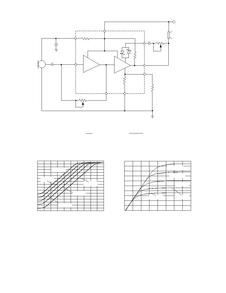
Fig. 1 Test Circuit
All resistors in ohms, all capacitors in farads unless otherwise stated.
Fig. 2 Functional Schematic
510 - 69 - 06
4
R
MIC
1.0
R
S
3.9K
6
ED1913
R
LAC
2
V =1.3VDC
1
4
3
5
R
E
56
21K
7
8
- A
R
0.1
50K
MPO
B
Cs=0.22
100K
R
VC
- B
All resistors in ohms, all capacitors in farads unless otherwise stated.
R
VC
R
LAC
// 21K
R
S
56 // R
E
Gain of Stage A = 20 log
Gain of Stage B = 20 log
Fig. 3 Typical Hearing Aid Application
-120
-100
-80 -60 -40 -20
INPUT (dBV)
-80 -70 -60 -50 -40
INPUT (dBV)
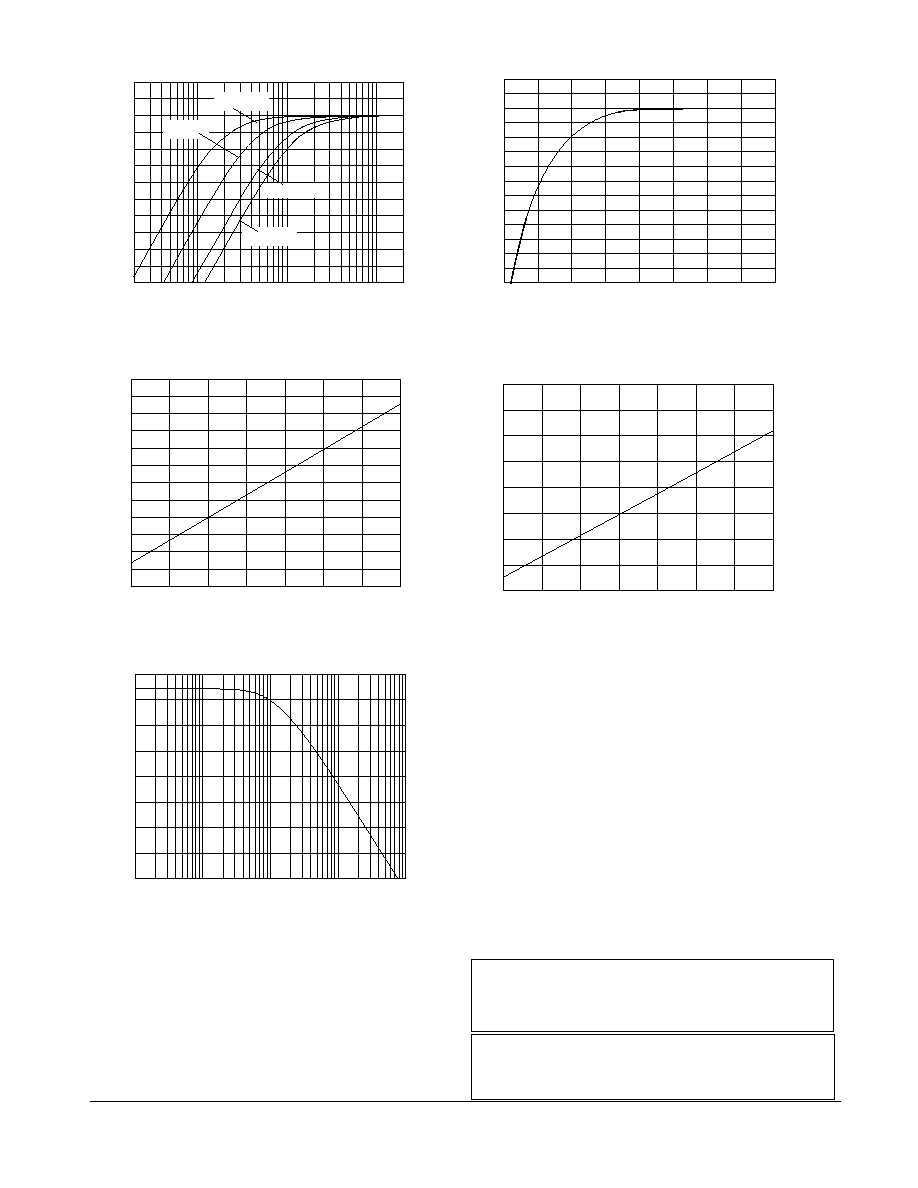
Fig. 5 I/O Curves at Various R
MPO
Values
0
-2
-4
-6
-8
-10
-12
-14
-16
-18
-20
R
VC
= 100K
R
VC
= 47K
R
VC
= 22K
R
VC
= 10K
R
VC
= 3.3K
R
MPO
= 50K
R
MPO
= 22K
R
MPO
= 10K
R
MPO
= 3.3K
R
MPO
= 0K
Fig. 4 I/O Curves at Various R
VC
Settings
-5
-15
-25
-35
-45
-55
-65
-75
-85
OUTPUT (
dBV)
OUTPUT (
dBV)
5
510 -69 - 06
-20 -10 0 10 20 30 40 50
TEMPERATURE (
o
C)
20
15
10
5
0
-5
-10
-15
-20
Fig. 9 Transducer Current vs Temperature
Fig. 7 Gain vs Supply Voltage
0.6 0.7 0.8 0.9 1 1.1 1.2 1.3 1.4
SUPPLY VOLTAGE (V)
C
S
= 0.1
C
S
= 0.047
C
S
= 0.22
Fig. 6 Closed Loop Frequency Response
with Various C
S
Values
C
S
= 0.033
-20 -10 0 10 20 30 40 50
TEMPERATURE (
o
C)
25
20
15
10
5
0
-5
-10
-15
-20
-25
-30
-35
10 100 1K 10K 100K
FREQUENCY (Hz)
Fig. 8 Amplifier Current vs Temperature
20
200
2K
20K
FREQUENCY (Hz)
10
0
-10
-20
-30
-40
-50
-60
4
0
-4
-8
-12
-16
-20
60
55
50
45
40
35
30
25
20
Fig. 10 Preamplifer Open Loop
Frequency Response
RELATIVE AMPLIFIER CURRENT (
µ
A)
RELATIVE TRANSDUCER CURRENT (
µ
A)
RELATIVE GAIN (
d
B
)
RELATIVE GAIN (
d
B
)
GAIN (
d
B
)
DOCUMENT IDENTIFICATION:
DATA SHEET
The product is in production. Gennum reserves the right to make
changes at any time to improve reliability, function or design, in
order to provide the best product possible.
Gennum Corporation assumes no responsibility for the use of any circuits described herein and makes no representations that they are free from patent infringement.
© Copyright October 1987 Gennum Corporation. All rights reserved. Printed in Canada.
REVISION NOTES:
Changes to standard packaging information.
GENNUM CORPORATION
MAILING ADDRESS:
P.O. Box 489, Stn. A, Burlington, Ontario, Canada L7R 3Y3
Tel. +1 (905) 632-2996 Fax +1 (905) 632-2814
SHIPPING ADDRESS:
970 Fraser Drive, Burlington, Ontario, Canada L7L 5P5
GENNUM JAPAN CORPORATION
C-101, Miyamae Village, 2-10-42 Miyamae, Suginami-ku, Tokyo 168-0081,
Japan Tel. +81 (3) 3334-7700 Fax: +81 (3) 3247-8839