
Document No. 510 - 78 - 06
GENNUM
C
O
R
P
O
R
A
T
I
O
N
Programmable Analog
Signal Processor
GP520A - DATA SHEET
Principle features of the preamp are the input impedance
100 k
and a gain of 14 dB.
The programmable filter block is composed of a low pass
and high pass filter which generates a range of high and
low pass corner frequencies. Although the control current
to this block varies linearly, linear to logarithmic conversion
is performed internally in order to adjust the corner frequencies
logarithmically. Both filters feature a 12 dB/octave rolloff
and unity gain.
The filters are followed by an AGC block. Up to 35 dB of
adjustable gain is provided as well as programmable
threshold and release time. The attack time of the AGC
block remains fixed and is independent of the release
time. The output current is driven into the preamp of the
clipper, thus, the AGC converts a voltage input into a
current output and is therefore, a transconductance block.
The next stage is an electronic MPO control peak "clipper"
providing electronic clipping of the signal and setting of
the maximum output level. The clipper output is also a
transconductance block and drives a 40 k
resistor (R
OUT 8
)
tied to the supply.
The input of the final stage is an inverting operational
amplifier. A feedback resistance of 240 k
is provided
internally and this final stage is thus configured as a
voltage drive output stage. The DC bias current through
the receiver is also programmable.
FEATURES
�
programmable parameters
- gain
- low pass filter
- high pass filter
- AGC threshold
- release time
- MPO
- receiver bias voltage
�
on-chip voltage regulator
�
typical gain 60 dB
�
voltage drive output stage
�
telecoil preamp
FUNCTIONAL BLOCK DIAGRAM
FULL WAVE
RECTIFIER
AVERAGING
CIRCUIT
THRESHOLD
AGC
Vcc
RF
LIN/LOG
CONVERTER
I
REF
LIN/LOG
CONVERTER
LIN/LOG
CONVERTER
R
2R
HP
FILTER
+
-
PREAMP
+
-
40K
R
IN14
10K
VOLTAGE
REGULATOR
R
R
14
13
9
18
15
19
22
24
26
27
1
3
5
7
8
10
11
17
4
23
2
25
16
21
20
6
GND
I
HP
I
LP
I
REF
I
REL
I
THRESH
I
GAIN
I
CLIP
I
BIAS
D
OUT
D
IN
C
OUT
B
OUT
B
IN
DELTA
OUT
C
AGC
RECT.
IN
BUFFER
OUT
BUFFER
IN
+
-
LP
FILTER
LPFB
HP
HPFB
A
OUT
V
CC
V
REG
A
IN
OUTPUT
-
+
R
OUT 8
12
P GND
C
COMP
31
30
C
CLIP
29
28
V
BIAS
50k
VC AMP
CLIPPER
All resistors in ohms, all capacitors in farads unless otherwise stated.
STANDARD PACKAGING
�
Chip (136 x 110 mils)
Au Bump
CIRCUIT DESCRIPTION
The GP520A is a programmable analog signal path IC
designed for use in hearing instruments. The GP520A's
programmable parameters are adjusted by external
programming currents, such as generated by the GP521.
The GP520A provides a 2.5
�
A reference current for use by
the GP521. Sixteen settings are possible in the GP521,
allowing the Programmable Current Sink (PCS) to sink
between 0 and 1.875 x I
REF
.
The GP520A is composed of five functional blocks. The
input preamp, a filter block, the AGC block, MPO clipper
and the output stage.
Revision Date: May 1998
GENNUM CORPORATION P.O. Box 489, Stn. A, Burlington, Ontario, Canada L7R 3Y3 tel. +1 (905) 632-2996
Web Site: www.gennum.com E-mail: hipinfo@gennum.com
2
510 - 78 - 06
27
1
2
3
4
5
6
7
8
9
10
11
12
14
26
25
24
23
22
21
20
19
18
17
16
15
GP520A
GND
I
HP
I
LP
I
REF
I
REL
I
THRESH
I
GAIN
I
CLIP
I
BIAS
D
OUT
D
IN
C
OUT
B
OUT
B
IN
DELTA OUT
C
AGC
RECT.IN
BUFFER OUT
BUFFER IN
LPFB
HP
HPFB
A
OUT
V
CC
V
REG
A
IN
P
GND
13
30
29
28
TEL-C
TEL-B
31
C
COMP
C
CLIP
ELECTRICAL CHARACTERISTICS
All parameters are measured at T
A
= 25
o
C
All gains are calculated from equation G = 20 LOG (
OUT/
IN) where
OUT and
IN are appropriate voltage or current increases.
All resistances are calculated according to equation R = (V
P
- V
Q
) / I
COND
where V
P
is voltage on the pad loaded with I
COND
current.
V
Q
- quiescent (unbias) voltage measured on the pad, (nothing connected to the pin).
V
P
is the actual voltage measured on the pad at given condition (where P is pad number).
For all graphs I
REF
is measured with 0.5V biased voltage on pin 16.
GENERAL
PARAMETER
SYMBOL
CONDITIONS
MIN TYP MAX UNITS
Amplifier Current
I
AMP
All PCS set to 15
-
600
-
�
A
Minimum Voltage
V
CC
1.1
-
-
V
Regulator Voltage (Pad 13)
V
REG
-
0.98
-
V
Short Circuit Current (Pad 13)
I
SC
S1 -- closed
-
2.0
-
mA
Current Reference (Pad 16)
I
R
-
2.5
-
�
A
Quiescent Voltage on Pad 14
V
Q14
600
-
-
mV
Quiescent Voltage on Pad 15
V
Q15
600
-
-
mV
Input Resistance (Pad 14)
R
IN 14
I
14
=
0.3
�
A
(S2 closed)(
Note 1
)
-
100
-
k
Output Swing High (Pad 15)
V
OH
V
14
=
0.8V
(S3 closed)(
Note 1
)
200
-
-
mV
Output Swing Low (Pad 15)
V
OL
V
1
=
0.4V (S3 closed)
-200
-
-
mV
Max Source Current (Pad 15)
I
SOURCE
V
14
=
0.8V (S3, S4 closed)
30
-
-
�
A
V
15
=
V
Q15
+100mV
Max Sinking Current (Pad 15)
I
SINK
V
14
=
0.4V (S3,S4 closed)
30
-
-
�
A
V
15
=
V
Q15
-100mV
Preamp Voltage Gain
GAIN V
14
=
V
Q14
�
10mV (S3 closed)
-
14
-
dB
NOTE: 1.
V
OL
= V
OH
= V
P15
� V
Q15
All switches remain OPEN unless otherwise stated in CONDITIONS column.
PARAMETER
VALUE / UNITS
Supply Voltage 5 V
Pad 3, 8, 10, 11, 13, 17 -0.1 V to V
CC
+ 0.1 V
Pad 1, 15, 16, 18, 19, 22, 24, 26
-0.1 V to V
REG
+ 0.1 V
Pad 4, 5, 7, 14, 20, 21, 23, 25, 27
-0.1 V to 0.7 V
Pad 2 V
REG
-0.7 V to V
REG
+ 0.1 V
ABSOLUTE MAXIMUM RATINGS
CURRENT REFERENCE
REGULATOR TESTS
PREAMPLIFIER
CAUTION
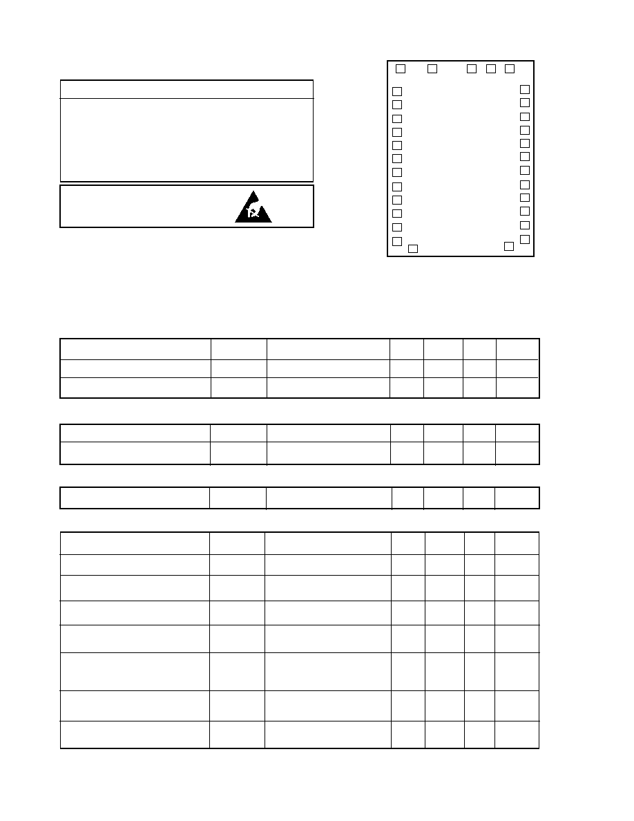
CLASS 1 ESD SENSITIVITY
CHIP PAD DIAGRAM

3
510 - 78 - 06
V
REG
3�3
S3
V19
S2
R
2R
R
13
9
18
19
22
5
7
11
21
20
6
GND
I
HP
I
LP
D
OUT
IN
LPFB
HP
HPFB
V
CC
P GND
12
V
CC
2k2
0.6 V
R
IN
I
HP
26
27 1
30
31
10K
B
OUT
B
AGC
C
68n
68n
10n 10n
LIN/LOG
CONVERTER
LIN/LOG
CONVERTER
+
-
HP
FILTER
+ -
V
REG
A
IN
V
CC
2k2
V15
-
+
-
+
1.3V
S4
-
+
S1
S2
S3
V14
I14
40K
R
IN14
10K
VOLTAGE
REGULATOR
14
13
9
15
5
7
11
6
GND
D
OUT
OUT
A
OUT
V
CC
P GND
12
3�3
26
27 1
10K
B
OUT
B
AGC
C
68n
68n
10n
10n
31
30
+
-
PREAMP
PARAMETER
SYMBOL
CONDITIONS
MIN
TYP
MAX
UNITS
Quiescent Voltage on Pad 18
V
Q18
-
650
-
mV
Quiescent Voltage on Pad 19
V
Q19
-
650
-
mV
Quiescent Voltage on Pad 20
V
Q20
-
550
-
mV
Maximum DC Current from Pad 19
I
HP MAX
I
HP
= 0
�
A
( S3 closed)
-
2
-
�
A
Minimum DC Current from Pad 19
I
HP MIN
I
HP
=1.875 x I
R
(S3 closed)
-
200
-
nA
Buffer Gain
GAIN V
19
= V
Q19
�
100mV
(S2 closed)
-
0
-
dB
Input Resistance Pad 20
R
IN20
I
HP
=
I
R
-
13
-
k
All switches remain OPEN unless otherwise stated in CONDITIONS column.
HIGH PASS FILTER
Fig. 2 High Pass Filter DC Test Circuit
Fig. 1 Preamplifier and Regulator Test Circuit
All resistors in ohms, all capacitors in
farads unless otherwise stated.
All resistors in ohms, all capacitors in
farads unless otherwise stated.

4
510 - 78 - 06
I
LP
S1
V
CC
2k2
V
REG
3�3
I
REF
R
R
13
9
22
24
26
27
1
11
16
21
6
GND
I
REF
D
OUT
OUT
10K
AGC
RECT.
IN
BUFFER
OUT
BUFFER
IN
+
-
LP
FILTER
LPFB
V
CC
P GND
12
LIN/LOG
CONVERTER
V26
-
+
-
+
V24
S2
S3
+1.3 V
0.6 V
R
IN
I
LP
C
68n
68n
10n
10n
5
7
B
B
IN
30
31
PARAMETER SYMBOL
CONDITIONS MIN TYP MAX UNITS
Quiescent Voltage on Pad 21
V
Q21
-
550
-
mV
Quiescent Voltage on Pad 22
V
Q22
-
650
-
mV
Quiescent Voltage on Pad 24
V
Q24
-
650
-
mV
Quiescent Voltage on Pad 26
V
Q26
-
650
-
mV
Maximum DC Current from Pad 22
I
LP MAX
I
LP
= 0
�
A (S1 closed)
-
2.0
-
�
A
Minimum DC Current from Pad 22
I
LP MIN
I
LP
=1.875 x I
R
(S1 closed)
-
0.7
-
�
A
Output Swing High (Pad 26)
V
OH
V
24
= V
Q24
+ 100mV (S2 closed)
(Note 1)
-
100
-
mV
Output Swing Low (Pad 26)
V
OL
V
24
= V
Q24
- 100mV (S2 closed )
(Note 1)
-
-100
-
mV
Max Sinking Current from Pad 26
I
SINK
V
24
= 0.4V; V
26
= V
Q26
- 100mV
30
-
-
�
A
(S2, S3 closed)
Max Sourcing Current to Pad 26
I
SOURCE
V
24
= 0.8V; V
26
= V
Q26
�
100mV
-30
-
-
�
A
(S2, S3 closed)
Buffer Gain
GAIN
V
26
= V
Q26
�
100mV
-
0
-
dB
Input Resistance (Pad 21)
R
IN21
I
LP
= I
R
-
13
-
k
NOTE: 1.
V
OH
= V
OL
= V
P26
- V
Q26
All switches remain OPEN unless otherwise stated in CONDITIONS column.
LOW PASS FILTER
Fig. 3 Low Pass Filter DC Test Circuit
All resistors in ohms, all capacitors in
farads, unless otherwise stated.

5
510 - 78 - 06
680p
V
CC
2k2
2n2
3�3
PINK
NOISE
GENERATOR
1n5
2n2
10�
LIN/LOG
CONVERTER
R
2R
HP
FILTER
+
-
PREAMP
+
-
40K
R
IN14
10K
VOLTAGE
REGULATOR
R
R
14
13
9
18
15
19
22
24
26
5
7
11
21
20
GND
I
HP
I
LP
D
OUT
IN
BUFFER
OUT
BUFFER
IN
+
-
LP
FILTER
LPFB
HP
HPFB
A
OUT
V
CC
A
IN
P GND
12
LIN/LOG
CONVERTER
0.6 V
0.6V
6
I
LP
I
HP
27
OUT
B
68n
TP
B
10K
68n
10n
10n
1
31
30
I
HP
= 1.875 x
I
R
Fig. 6 Low Pass Filter Corner Frequency vs
I
LP
Current
(Note 1) (Fig.4 Test Circuit)
NOTES: 1.
Corner frequency calculated in reference to signal at 3 kHz
10k
1k
100
80
0 0.25 0.5 0.75 1 1.25 1.5 1.75 2
NORMALIZED
I
HP
/
I
R
CURRENT
Fig. 5 High Pass Filter Corner Frequency vs
I
HP
Current
(Note 1) (Fig.4 Test Circuit)
10k
1k
700
0 0.25 0.5 0.75 1 1.25 1.5 1.75 2
NORMALIZED
I
HP
/
I
R
CURRENT
Fig. 4 AC Test Circuit for High & Low Pass Filters
CORNER FREQUENCY (HZ)
CORNER FREQUENCY (Hz)
All resistors in ohms, all capacitors in
farads, unless otherwise stated.