
GENNUM CORPORATION P.O. Box 489, Stn. A, Burlington, Ontario, Canada L7R 3Y3
Tel. +1 (905) 632-2996 Fax. +1 (905) 632-5946 E-mail: info@gennum.com
www.gennum.com
Revision Date: May 2005
Document No. 15879 - 4
DATA SHEET
GS15
03
FEATURES
� complies with SMPTE 292M and SMPTE 299M
� single chip HD embedded audio solution
� operates as an embedded audio multiplexer or
demultiplexer
� full support for 48kHz synchronous 24-bit audio
� support for 8 channels of audio per device
� cascadable architecture supports up to 16 audio channels
� integrated scrambler/descrambler and word alignment
� CRC error detection and insertion
� audio control packet insertion and extraction
� arbitrary data packet insertion and extraction
� 3.3V power supply with 5V tolerant I/O
� 144 pin LQFP package
APPLICATIONS
HD SDI Embedded Audio
DESCRIPTION
The GS1503 is a highly integrated, single chip solution for
embedding/extracting digital audio streams into and out of
high definition digital video signals. The GS1503 supports
insertion/extraction of 24-bit synchronous audio data with a
48kHz sample rate. Audio signals with different sample
rates may be converted to 48kHz by using audio sample
rate converters before or after the GS1503.
Each GS1503 supports all processing required for
embedding/extracting up to eight digital audio channels in
the horizontal ancillary data space of the video chroma
channel. Two GS1503's can be cascaded for insertion/
extraction of up to 16 audio channels with no external glue
logic.
The GS1503 supports embedding/extracting of audio
control and arbitrary data packets in the horizontal ancillary
data space of the video luma channel. It also supports line
CRC detection and insertion.
The GS1503 supports HD video standards at 74.25MHz
and 74.25/1.001MHz rates. It has an on chip SMPTE
compliant scrambler/de-scrambler, and integrated word
alignment. Use the GS1503 with Gennum's GS1545 or
GS1522 for two chip HD SDI receive or transmit solutions.
The GS1503 operates from a single 3.3V power supply with
5V tolerant I/O and is packaged in a 144 pin LQFP
package.
MULTIPLEX MODE BLOCK DIAGRAM
ORDERING INFORMATION
PART NUMBER
PACKAGE
TEMPERATURE
GS1503-CFZ
144 pin LQFP
0�C to 70�C
VIN[19:0]
20
Video Detection &
Synchronization
20
VOUT[19:0]
ANCI Timing
Generation
4
VIDEO_DET
OPERATE
ERROR
CRC_ERR
De-scrambler &
Word Alignment
20
CRC Inserter &
Scrambler
TRS
Inserter
20
DSCBYPASS
SCRBYPASS
Host
Interface
Audio
Input
Interface
AIN1/2
AIN3/4
AIN5/6
AIN7/8
CPUADR[8:0]
CPUDAT[7:0]
4
9
8
2
WCINA/B
3
Arbitrary
Packet
Mux
Audio
Packet
Mux
Control
Packet
Mux
HOST INTERFACE
HOST INTERFACE
8
PKT[7:0]
PKTEN
PKTENO
4
VM[3:0]
MUTE
AM[1:0]
20
EXTF
EXTH
2
CPUCS, CPUWE,
CPURE
GS1503
HD EMBEDDED AUDIO CODEC

15879 - 4
2 of 83
GS15
03
DEMULTIPLEX MODE BLOCK DIAGRAM
ABSOLUTE MAXIMUM RATINGS
PARAMETER
VALUE
Supply Voltage
-0.3V to 4.0V
Input Voltage (any input)
-0.3 to 5.5V
Operating Temperature
0�C to 70�C
Storage temperature
-65�C to 150�C
Lead Temperature (soldering, 10 sec.)
230�C
DC ELECTRICAL CHARACTERISTICS
T
A
= 0�C to 70�C unless otherwise shown.
PARAMETER
SYMBOL
CONDITIONS
MIN
TYP
MAX
UNITS
Supply Voltage
V
DD
3.3V operating range
3.0
3.3
3.6
V
Supply Current
I
DD
V
DD
= 3.3V
270
mA
Input Current
I
IN
-1
-
1
�A
Hi-Z Output Leakage Current
I
OZ
-1
-
1
�A
Output Voltage, Logic High
V
OH
I
OH
= -12mA
V
DD
-0.4
-
-
V
Output Voltage, Logic Low
V
OL
I
OL
= 12mA
-
-
0.4
V
Input Voltage, Logic High
V
IH
TTL Level
2.0
-
-
V
Input Voltage, Logic Low
V
IL
TTL Level
-
-
0.8
V
Input Capacitance
C
I
f = 1MHz, V
DD
= 0V
-
-
10
pF
Output Capacitance
C
O
f = 1MHz, V
DD
= 0V
-
-
10
pF
I/O Capacitance
C
IO
f = 1MHz, V
DD
= 0V
-
-
10
pF
VIN[19:0]
20
Video Detection &
Synchronization
20
VOUT[19:0]
Delete
ANCI
ANCI
ANCI Timing
Generation
4
VIDEO_DET
OPERATE
ERROR
CRC_ERR
MUTE
De-scrambler &
Word Alignment
20
CRC Inserter &
Scrambler
20
DSCBYPASS
SCRBYPASS
Host
Interface
CPUADR[8:0]
CPUDAT[7:0]
9
8
3
PKT[7:0]
Arbitrary
Packet
Demux
Audio
Output
Interface
4
8
AOUT1/2
AOUT3/4
AOUT5/6
AOUT7/8
2
WCOUTA/B
PKTEN
Audio
Packet
Demux
Control
Packet
Demux
HOST INTERFACE
HOST INTERFACE
4
VM[3:0]
AM[1:0]
2
CPUCS, CPUWE,
CPURE
15879 - 4
3 of 83
GS15
03
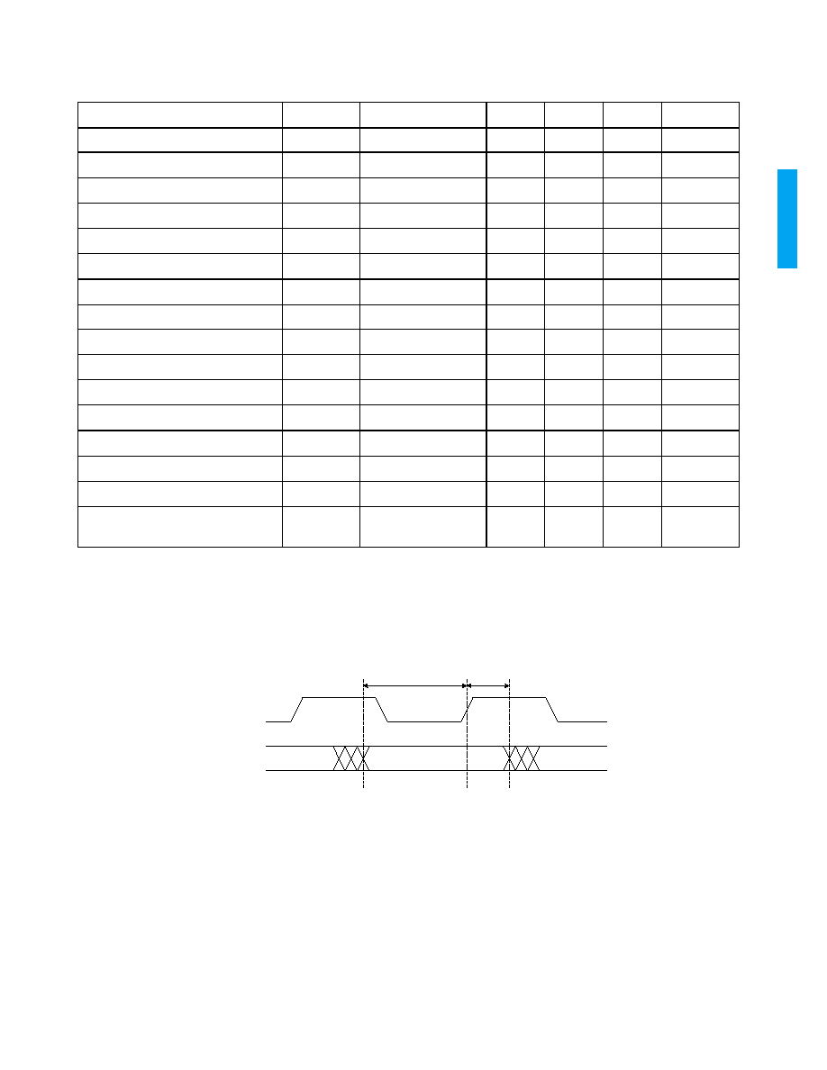
Fig. 1 Video Data Input Setup & Hold Time
AC ELECTRICAL CHARACTERISTICS
V
DD
= 3.3V � 5%, T
A
= 0�C to 70�C unless otherwise shown.
PARAMETER
SYMBOL
CONDITIONS
MIN
TYP
MAX
UNITS
Video Clock Frequency
-
74.25
80
MHz
Video Clock Pulse Width Low
t
VPWL
5.0
-
-
ns
Video Clock Pulse Width High
t
VPWH
5.0
-
-
ns
Video Input Data Setup Time
t
VS
3.5
-
-
ns
Video Input Data Hold Time
t
VH
1.0
-
-
ns
Video Output Data Delay Time
t
VOD
With 10pF loading
-
-
8.5
ns
Video Output Data Hold Time
t
VOH
With 10pF loading
1.0
-
-
ns
Audio Clock Frequency
-
6.144
-
MHz
Audio Clock Pulse Width Low
t
APWL
60
-
-
ns
Audio Clock Pulse Width High
t
APWH
60
-
-
ns
Audio Input Data Setup Time
t
AS
10.5
-
-
ns
Audio Input Data Hold Time
t
AH
1.0
-
-
ns
Audio Output Data Delay Time
t
AOD
With 10pF loading
-
-
20.0
ns
Audio Output Data Hold Time
t
AOH
With 10pF loading
1.0
-
-
ns
Reset Pulse Width
t
RESET
1
-
-
ms
Device Latency
Multiplexer Mode
Demultiplexer Mode
53
53
53
53
53
53
PCLKs
VCLK
Data*
* VIN[19:0],
EXTF, EXTH, PKTEN, PKT[7:0]
tVS
tVH

15879 - 4
4 of 83
GS15
03
Fig. 2 Video Data Output Delay & Hold Time
Fig. 3 Audio Data Input Setup & Hold Time
Fig. 4 Audio Data Output Delay & Hold Time
Fig. 5 Reset Timing
VCLK
Data*
* VOUT[19:0], EXTF, EXTH, PKTEN, PKT[7:0]
tVOH tVOD
ACLKA/B
Data*
* WCINA, AIN1/2, AIN3/4, WCINB, AIN5/6, AIN7/8
tAS
tAH
ACLKA/B
Data*
* AOUT1/2, AOUT3/4, AOUT5/6, AOUT7/8
tAOH
tAOD
VDD
RESET
tRESET
VDD(min)
tRESET

15879 - 4
5 of 83
GS15
03
HOST INTERFACE
Fig. 6 Host Interface Mode A Timing (CPU_SEL set HIGH)
Mode A (CPU_SEL set HIGH)
PARAMETER
NUMBER
MIN
TYP
MAX
UNITS
Read Cycle Time
1
50
-
-
ns
Read Chip Select Setup Time
2
0
-
-
ns
Read Address Setup Time
3
15
-
-
ns
Read Data Output Delay Time
4
-
-
15
ns
Read Data Hold Time
5
0
-
-
ns
Write Cycle Time
6
50
-
-
ns
Write Chip Select Setup Time
7
10
-
-
ns
Write Address Setup Time
8
10
-
-
ns
Write Data Setup Time
9
10
-
-
ns
Write Data Hold Time
10
0
-
-
ns
CPUADR[8:0]
CPUDAT[7:0]
CPUCS
CPURE
Valid Data
Valid Data
1
3
4
5
CPUWE
Address
Address
2
6
7
8
9
10
Read Cycle
Write Cycle