
GENNUM CORPORATION P.O. Box 489, Stn. A, Burlington, Ontario, Canada L7R 3Y3
Tel. +1 (905) 632-2996 Fax. +1 (905) 632-5946 E-mail: info@gennum.com
www.gennum.com
Revision Date: March 2000
Document No. 522 - 05 - 02
PRELIMINARY DATA SHEET
G
S
1
504
HD-LINX
TM
GS1504
HDTV Adaptive Equalizer
FEATURES
∑ SMPTE 292M compliant
∑ Automatic, adjustment free cable equalization for
1.485Gb/s HDTV signals
∑ Differential serial outputs capable of driving 50
loads
∑ Typically equalizes 100m of Belden 8281 or 150m of
Belden 1694 high quality co-axial cable
∑ Cable Length Indication
∑ Output Mute
∑ Maximum Cable Length Adjust
∑ Low power
∑ Minimal external components
∑ Single +5V or -5V power supply operation
APPLICATIONS
1.485Gb/s HDTV Serial Digital Receiver Interfaces for
Routers, Distribution Amplifiers, Switchers, and other
receiving equipment.
DESCRIPTION
The GS1504 is a high performance cable equalizer
designed to equalize HDTV component signal conforming
to SMPTE 292M. The adaptive cable equalizer is capable of
equalizing up to 100m of Belden 8281 co-axial cable.
The GS1504 features DC restoration for immunity to the DC
content in pathological test patterns. The device also
incorporates a Cable Length Indicator signal that provides
an indication of the amount of cable being equalized.
A voltage programmable mute threshold (MCLADJ) is
included to allow muting of the GS1504 output when a
selected cable length is reached. This feature allows the
GS1504 to distinguish between low amplitude HD SDI
signals and noise at the input of the device. The CD/Mute
pin provides an indication of the GS1504 mute status in
addition to functioning as a mute control input. The output
of the GS1504 may be forced to an active or a mute
condition by applying a voltage to the CD/Mute pin.
The GS1504 is a low power device that operates from a
single 5V power supply. The GS1504 is packaged in a
16 pin narrow SOIC and does not need external pull-up
resistors.
BLOCK DIAGRAM
ORDERING INFORMATION
PART NUMBER
PACKAGE
TEMPERATURE
GS1504-CKD
16 pin narrow SOIC
0∞C to 70∞C
GS1504-CTD
16 pin Tape and Reel
0∞C to 70∞C
CABLE LENGTH INDICATOR/ADJUSTOR
CARRIER DETECT
MUTE
MCLADJ
CLI
CD/MUTE
EQUALIZER
DC
RESTORE
OUTPUT
AGC
SDI
SDI
SDO
SDO
PATENT PENDING
522 - 05 - 02
2
G
S
150
4
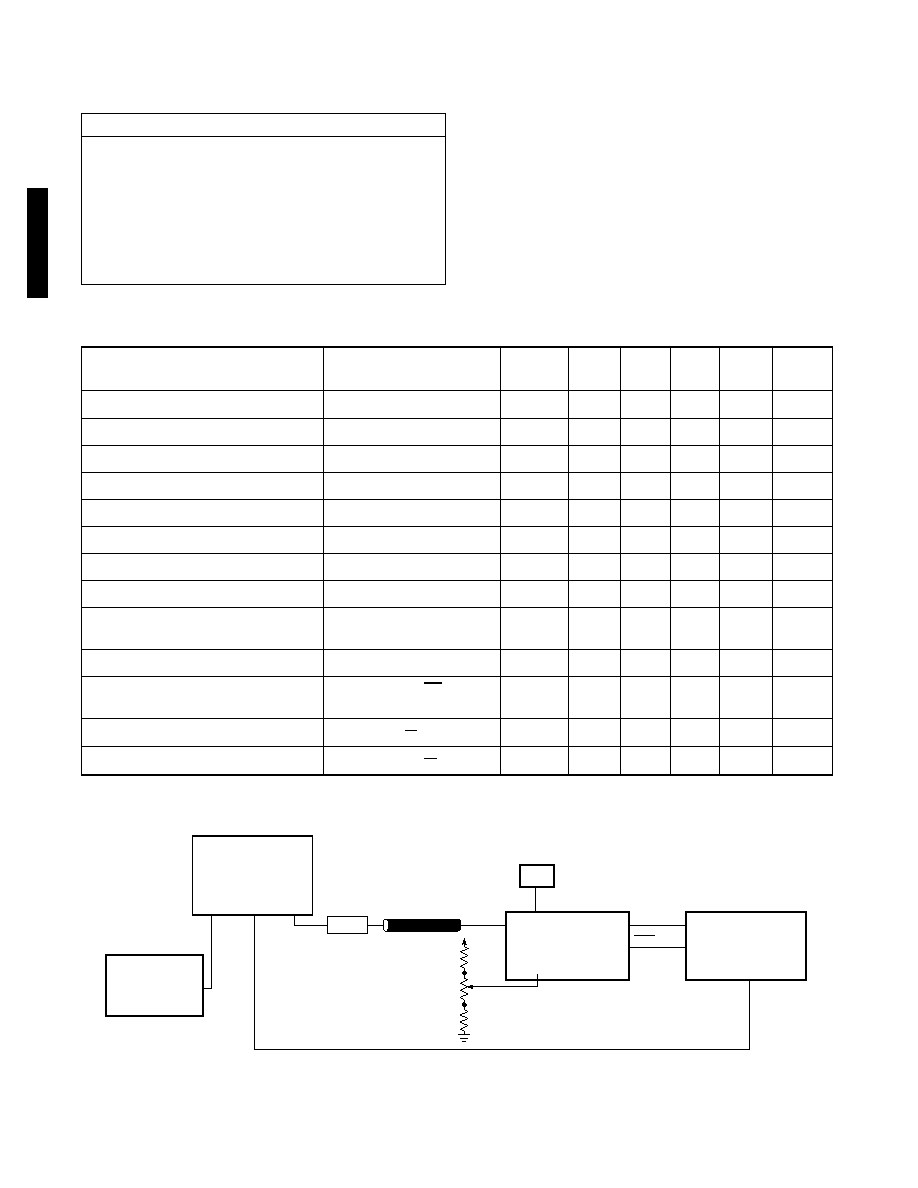
Fig. 1 Test Setup
ABSOLUTE MAXIMUM RATINGS
T
A
= 25∞C unless otherwise indicated
PARAMETER
VALUE
Supply Voltage
5.5V
Input Voltage Range (any input)
-0.3 to (V
CC
+0.3)V
Operating Temperature Range
0∞C to 70∞C
Storage Temperature
-65∞C to 150∞C
Power Dissipation
300mW
Lead Temperature (soldering, 10 sec)
260∞C
Input ESD Voltage
2000V
DC ELECTRICAL CHARACTERISTICS
V
CC
= 5V, V
EE
= 0V, T
A
= 0∞C to 70∞C, Data Rate = 1.485Gb/s
PARAMETER
CONDITIONS
SYMBOL
MIN
TYP
MAX
UNITS
TEST
LEVELS
Positive Supply Voltage
V
CC
4.75
5.00
5.25
V
1
Power Consumption
-
250
-
mW
1
Supply Current
-
50
65.0
mA
1
Output CM Voltage
3.75
4
4.25
V
1
Input DC Voltage
Internal Bias. See Figure 2
-
2.7
-
V
1
CLI DC Voltage (0m)
CLI Output for 0m Cable
-
3.3
-
V
4
CLI DC Voltage (no signal input)
0.9
1.3
1.7
V
1
Cable Length Indicator Range
0 - Max m
CLI
-
2
-
V
2
MCLADJ DC Voltage
MCLADJ Input Voltage
Required to Mute Output
2.80
3.1
3.4
V
1
MCLADJ Range
(max cable to 0m)
1
V
2
Mute DC Voltage
Output Voltage of CD/Mute
when Output is Active
1.5
1.8
2.1
V
1
Voltage Required to Force Outputs to Mute
Min to Mute; V
CD/Mute
4.2
V
2
Voltage Required to Force Outputs Active
Max to Activate; V
CD/Mute
3.8
V
2
TEST LEVELS: 1. 100% tested at 25∞C. 2. Guaranteed by design. 3. Correlated Value. 4. Using EB1504
GigaBERT
1400
EXT.
CLOCK
CLOCK
OUT
DATA
OUT
EXT.
CLOCK
1.485GHz
GS1504
EVAL. BOARD
TDS 820
CH. 1
CH. 2
OUT
IN
OUT
EXT. TRIGGER
MCLADJ
CLI
DVM
50/75
10k
2k
15k
8281 or 1694A CABLE
522 - 05 - 02
3
G
S
1
504
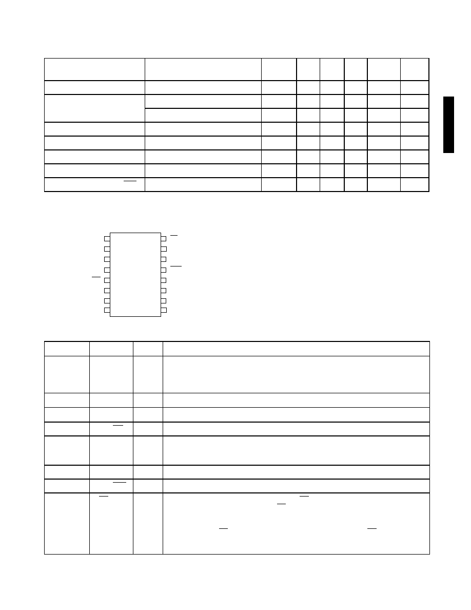
PIN CONNECTIONS
AC ELECTRICAL CHARACTERISTICS
V
CC
= 5V, V
EE
= 0V, T
A
= 0∞C to 70∞C, Data Rate = 1.485Gb/s
PARAMETER
CONDITIONS
SYMBOL
MIN
TYP
MAX
UNITS
TEST
LEVEL
Jitter
100m (8281), PRN and pathological
-
80
135
ps p-p
1
Equalization
Belden 8281
-
100
-
m
1
Belden 1694
-
150
-
m
3
Output Rise/Fall Time
20% - 80%
-
130
270
ps
1
Input Resistance
Single Ended
-
2.8
.
k
2
Input Capacitance
Single Ended
-
1
-
pF
2
Output Resistance
Single Ended
-
50
-
2
Output Signal Swing SDO, SDO Into
50
Loads; See Figure 21.
160
200
240
mVp-p
1
TEST LEVELS: 1. 100% tested at 25∞C. 2. Guaranteed by design. 3. Correlated Value. 4. Using EB1504
1
2
3
4
5
6
7
8
16
15
14
13
12
11
10
9
CLI
V
CC
V
EE
SDI
SDI
V
EE
MCLADJ
NC
CD/MUTE
V
CC
V
EE
SDO
SDO
V
EE
NC
NC
GS1504
TOP
VIEW
PIN DESCRIPTIONS
NUMBER
SYMBOL
TYPE
DESCRIPTION
1
CLI
O
Cable Length Indication
. Provides a voltage output representing the amount of cable being
equalized. See figures 19 and 20. The CLI voltage is an approximation of the cable length
being equalized. It is intended as a guide for troubleshooting the initial design and not as an
accurate indication of cable length.
2, 15
V
CC
I
Most positive supply voltage.
3, 6, 11, 14
V
EE
I
Most negative supply voltage.
4, 5
SDI, SDI
I
Differential Input Pins
. AC coupled termination is recommended.
7
MCLADJ
I
Adjusts the maximum amount of cable to be equalized (from 0m to the maximum cable
length). The output is muted (latched to the last state) when the maximum cable length is
reached. To achieve maximum cable length, this pin should be left open. See figures 10 - 12.
8, 9, 10
NC
-
No Connect
. Do not connect these pins to supply or ground.
12, 13
SDO, SDO
O
Differential Serial Data Output Pins
, with 50
output resistance.
16
CD/Mute
I/O
Carrier Detect/Mute Indicator/Control
. When the CD/Mute output is low, the carrier is present
and the data output is active. When the CD/Mute output is high, the carrier is not present and
the data output is muted (latched to the last state). This indicates that the maximum cable
length as set by MCLADJ has been reached.
The above default CD/Mute function can be overwritten as follows: if the CD/Mute pin is tied
to ground the data output will not mute and the MCLADJ setting is overwritten. If the mute pin
is tied high, the data output will always mute and the MCLADJ setting is overwritten.
522 - 05 - 02
4
G
S
150
4
INPUT/OUTPUT CIRCUITS
All resistors in ohms, all capacitors in farads, unless otherwise shown.
Fig. 2 Input Equivalent Circuit
Fig. 3 MCLADJ Equivalent Circuit
Fig. 4 Output Circuit
Fig. 5 CLI Output Circuit
Fig. 6 CD/Mute Circuit
6k
7k
6k
7k
RC
SDI
SDI
V
CC
MCLADJ
40k
42µ
+
-
50
50
SDO
SDO
10k
10k
V
CC
CLI
-
+
10k
20k
OUTPUT
STAGE
MUTE
CONTROL
V
CC
CD/MUTE
522 - 05 - 02
5
G
S
1
504
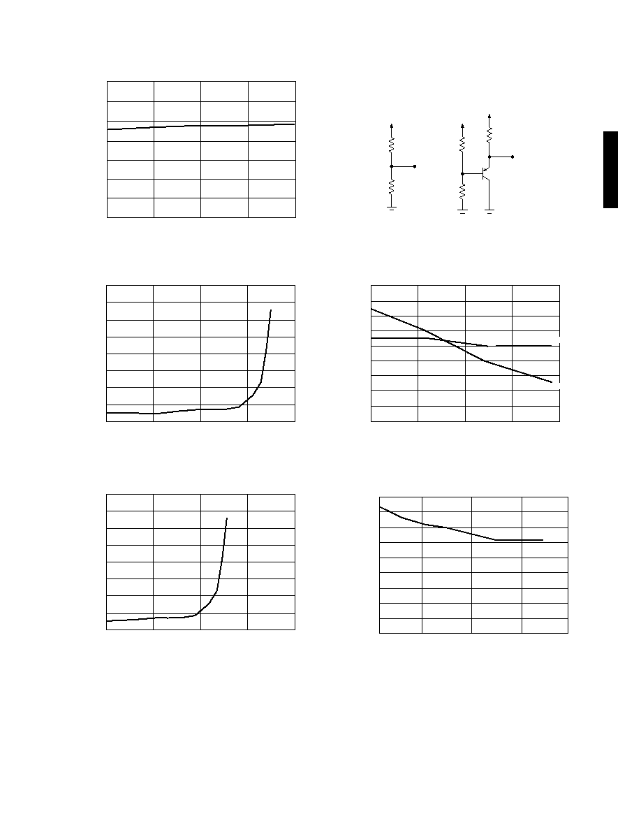
TYPICAL PERFORMANCE CURVES (unless otherwise shown, V
CC
= 5V, T
A
= 25∞C)
Fig. 7 Power Consumption
Fig. 8 Typical Peak to Peak Jitter, PRN 2
23
-1, Belden 1694A
Fig. 9 Typical Peak to Peak Jitter, PRN 2
23
-1, Belden 8281
Fig. 10 Temperature Compensation of MCLADJ
Fig. 11 Typical 1694A Cable Length vs. Temperature
Fig. 12 MCLADJ Input Voltage vs 1694A Cable Length
350
300
250
200
150
100
50
0
0 20 40 60 80
TEMPERATURE (∞C)
POWER CONSUMPTION (mW)
800
700
600
500
400
300
200
100
0
0 50 100 150 200
CABLE LENGTH (m)
JITTER (ps)
800
700
600
500
400
300
200
100
0
0 50 100 150 200
CABLE LENGTH (m)
JITTER (ps)
MCLADJ
MCLADJ
Uncompensated
MCLADJ
Temperature Compensated
MCLADJ
102
100
98
96
94
92
90
88
86
84
0 20 40 60 80
TEMPERATURE (∞C)
Uncompensated
CABLE LENGTH (m)
Compensated
90
80
70
60
50
40
30
20
10
0
CABLE LENGTH (m)
VOL
T
AGE NORMALIZED TO V
CC
(%)
0 50 100 150 200