 | –≠–ª–µ–∫—Ç—Ä–æ–Ω–Ω—ã–π –∫–æ–º–ø–æ–Ω–µ–Ω—Ç: GS1532_H | –°–∫–∞—á–∞—Ç—å:  PDF PDF  ZIP ZIP |

GENNUM CORPORATION P.O. Box 489, Stn. A, Burlington, Ontario, Canada L7R 3Y3
Tel. +1 (905) 632-2996 Fax. +1 (905) 632-5946 E-mail: info@gennum.com
www.gennum.com
Revision Date: September 2002
Document No. 21498 - 0
PRELIMINARY DATA SHEET
G
S
1
532
KEY FEATURES
KEY FEATURES
KEY FEATURES
KEY FEATURES
∑ DVB-ASI support including 8b/10b coding and sync
word insertion
∑ SMPTE 292M and SMPTE 259M-C compliant
scrambling and NRZI coding (with bypass)
∑ CRC calculation and insertion
∑ line number calculation and insertion
∑ TRS calculation and insertion
∑ illegal code re-mapping
∑ 20 bit / 10 bit CMOS parallel input data bus
∑ 148.5MHz / 74.25MHz / 27MHz / 13.5MHz parallel
digital input
∑ EDH generation and insertion
∑ adjustable loop bandwidth
∑ 1.8V core power supply and 3.3V charge pump power
supply
∑ 3.3V digital I/O supply
∑ JTAG test interface
∑ small footprint compatible with GS1560, GS1561,
GS9060 and GS9062
∑ low power operation (typically 460mW for HD)
APPLICATIONS
APPLICATIONS
APPLICATIONS
APPLICATIONS
∑
SMPTE 292M Serial Digital Interfaces
∑
SMPTE 259M-C Serial Digital Interfaces
∑
DVB-ASI Serial Digital Interfaces
DESCRIPTION
DESCRIPTION
DESCRIPTION
DESCRIPTION
The GS1532 is a multi-standard serializer with an integrated
cable driver. When used in conjunction with the GO1525
voltage controlled oscillator, a transmit solution for HD-SDI,
SD-SDI and DVB-ASI applications can be realized.
This device performs the functions of parallel to serial
conversion, scrambling as per SMPTE 292M/259M-C and
NRZ-to-NRZI conversion. The SMPTE scrambler may
optionally be bypassed to support the transmission of other
coding schemes.
In addition, the device can insert TRS signals, calculate and
insert line numbers and CRC's, re-map illegal code words
and insert SMPTE 352M payload identifier packets. All
processing features are optional and may be enabled/
disabled via external control pin(s) and/or host interface
programming.
The GS1532 may also be used in data pass-through mode
where no processing of the data is performed.
Parallel data inputs are provided in both 10-bit multiplexed
and 20-bit demultiplexed format for HD and SD signal rates.
An associated parallel clock input signal is provided
operating at: 148.5 or 148.5/1.001MHz, (HDTV 10-bit
multiplexed input); 74.25 or 74.25/1.001MHz, (HDTV 20-bit
demultiplexed input); 27MHz, (SDTV 10-bit multiplexed
input); and 13.5MHz, (SDTV 20-bit demultiplexed input).
The integrated cable driver features an output mute on loss
of parallel clock, high impedance mode, adjustable signal
swing, and automatic dual slew rate selection depending
on HD/SD operational requirements.
The device may also be configured for DVB-ASI operation
where it will insert K28.5 sync words and 8b/10b encode
the data stream prior to transmission.
GS1532
GS1532
GS1532
GS1532
Serializer for
Serializer for
Serializer for
Serializer for
HD-SDI, SD-SDI and DVB-ASI
HD-SDI, SD-SDI and DVB-ASI
HD-SDI, SD-SDI and DVB-ASI
HD-SDI, SD-SDI and DVB-ASI

GENNUM CORPORATION
21498 - 0
2
G
S
1
532
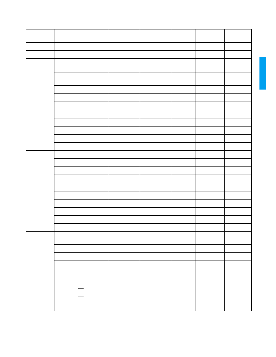
GS1532 FUNCTIONAL BLOCK DIAGRAM
GS1532 FUNCTIONAL BLOCK DIAGRAM
GS1532 FUNCTIONAL BLOCK DIAGRAM
GS1532 FUNCTIONAL BLOCK DIAGRAM
SDO
SDO
SDO_EN/DIS
RSET
CP_CAP
H
V
F
DIN[19:0]
IOPROC_EN/DIS
DVB_ASI
I/O
Buffer
&
demux
SMPTE
352M
generation
TRS insertion,
Line number
insertion,
CRC insertion,
data blank, code-
re-map and
flywheel
dvb-asi
bypass
RESET_TRST
POR
power on
reset
HOST Interface /
JTAG test
CS_TMS
SCLK_TCK
SDIN_TDI
SDOUT_TDO
JT
AG/HOST
LOCKED
V
CO
VCO
LF
LB_CONT
VCO_VCC
VCO_GND
SD/HD
20 bit/10 bit
DVB-ASI sync
word insert &
8b/10b encode
EDH
generation
& SMPTE
scramble
PCLK
BLANK
DETECT_TRS
SMPTE_BYP
ASS
Phase detctor, charge
pump, VCO control &
power supply
P
S
sd/hd

GENNUM CORPORATION
21498 - 0
3
G
S
1
532
TABLE OF CONTENTS
TABLE OF CONTENTS
TABLE OF CONTENTS
TABLE OF CONTENTS
1. PIN OUT
1. PIN OUT
1. PIN OUT
1. PIN OUT . . . . . . . . . . . . . . . . . . . . . . . . . . . . . . . . . . . . . . . . . . . . . . . . . . . . . . . . . . . . . . . . . . . . . . . . . . . . . . . . . 4
1.1 PIN ASSIGNMENT
. . . . . . . . . . . . . . . . . . . . . . . . . . . . . . . . . . . . . . . . . . . . . . . . . . . . . . . . . . . . . . . . 4
1.2 PIN DESCRIPTIONS
. . . . . . . . . . . . . . . . . . . . . . . . . . . . . . . . . . . . . . . . . . . . . . . . . . . . . . . . . . . . . 5-12
2. ELECTRICAL CHARACTERISTICS
2. ELECTRICAL CHARACTERISTICS
2. ELECTRICAL CHARACTERISTICS
2. ELECTRICAL CHARACTERISTICS . . . . . . . . . . . . . . . . . . . . . . . . . . . . . . . . . . . . . . . . . . . . . . . . . . . . . . . . . . . 13
2.1 ABSOLUTE MAXIMUM RATINGS
. . . . . . . . . . . . . . . . . . . . . . . . . . . . . . . . . . . . . . . . . . . . . . . . . . . . . 13
2.2 DC ELECTRICAL CHARACTERISTICS
. . . . . . . . . . . . . . . . . . . . . . . . . . . . . . . . . . . . . . . . . . . . . . . . . 14
2.3 AC ELECTRICAL CHARACTERISTICS
. . . . . . . . . . . . . . . . . . . . . . . . . . . . . . . . . . . . . . . . . . . . . . . . . 15
2.4 INPUT/OUTPUT CIRCUITS
. . . . . . . . . . . . . . . . . . . . . . . . . . . . . . . . . . . . . . . . . . . . . . . . . . . . . . . . . 16
2.5 HOST INTERFACE
. . . . . . . . . . . . . . . . . . . . . . . . . . . . . . . . . . . . . . . . . . . . . . . . . . . . . . . . . . . . . 17-25
3. DETAILED DESCRIPTION
3. DETAILED DESCRIPTION
3. DETAILED DESCRIPTION
3. DETAILED DESCRIPTION . . . . . . . . . . . . . . . . . . . . . . . . . . . . . . . . . . . . . . . . . . . . . . . . . . . . . . . . . . . . . . . . 26-30
4. APPLICATION REFERENCE DESIGN
4. APPLICATION REFERENCE DESIGN
4. APPLICATION REFERENCE DESIGN
4. APPLICATION REFERENCE DESIGN . . . . . . . . . . . . . . . . . . . . . . . . . . . . . . . . . . . . . . . . . . . . . . . . . . . . . . . . 31
4.1 TYPICAL APPLICATION CIRCUIT
. . . . . . . . . . . . . . . . . . . . . . . . . . . . . . . . . . . . . . . . . . . . . . . . . . . . 31
5. REFERENCES
5. REFERENCES
5. REFERENCES
5. REFERENCES . . . . . . . . . . . . . . . . . . . . . . . . . . . . . . . . . . . . . . . . . . . . . . . . . . . . . . . . . . . . . . . . . . . . . . . . . . . 32
6. PACKAGE & ORDERING INFORMATION
6. PACKAGE & ORDERING INFORMATION
6. PACKAGE & ORDERING INFORMATION
6. PACKAGE & ORDERING INFORMATION . . . . . . . . . . . . . . . . . . . . . . . . . . . . . . . . . . . . . . . . . . . . . . . . . . . . . 32
6.1 PACKAGE DIMENSIONS
. . . . . . . . . . . . . . . . . . . . . . . . . . . . . . . . . . . . . . . . . . . . . . . . . . . . . . . . . . . 32
6.2 ORDERING INFORMATION
. . . . . . . . . . . . . . . . . . . . . . . . . . . . . . . . . . . . . . . . . . . . . . . . . . . . . . . . . 32
7. REVISION HISTORY
7. REVISION HISTORY
7. REVISION HISTORY
7. REVISION HISTORY . . . . . . . . . . . . . . . . . . . . . . . . . . . . . . . . . . . . . . . . . . . . . . . . . . . . . . . . . . . . . . . . . . . . . . 33
GENNUM CORPORATION
21498 - 0
4
G
S
1
532
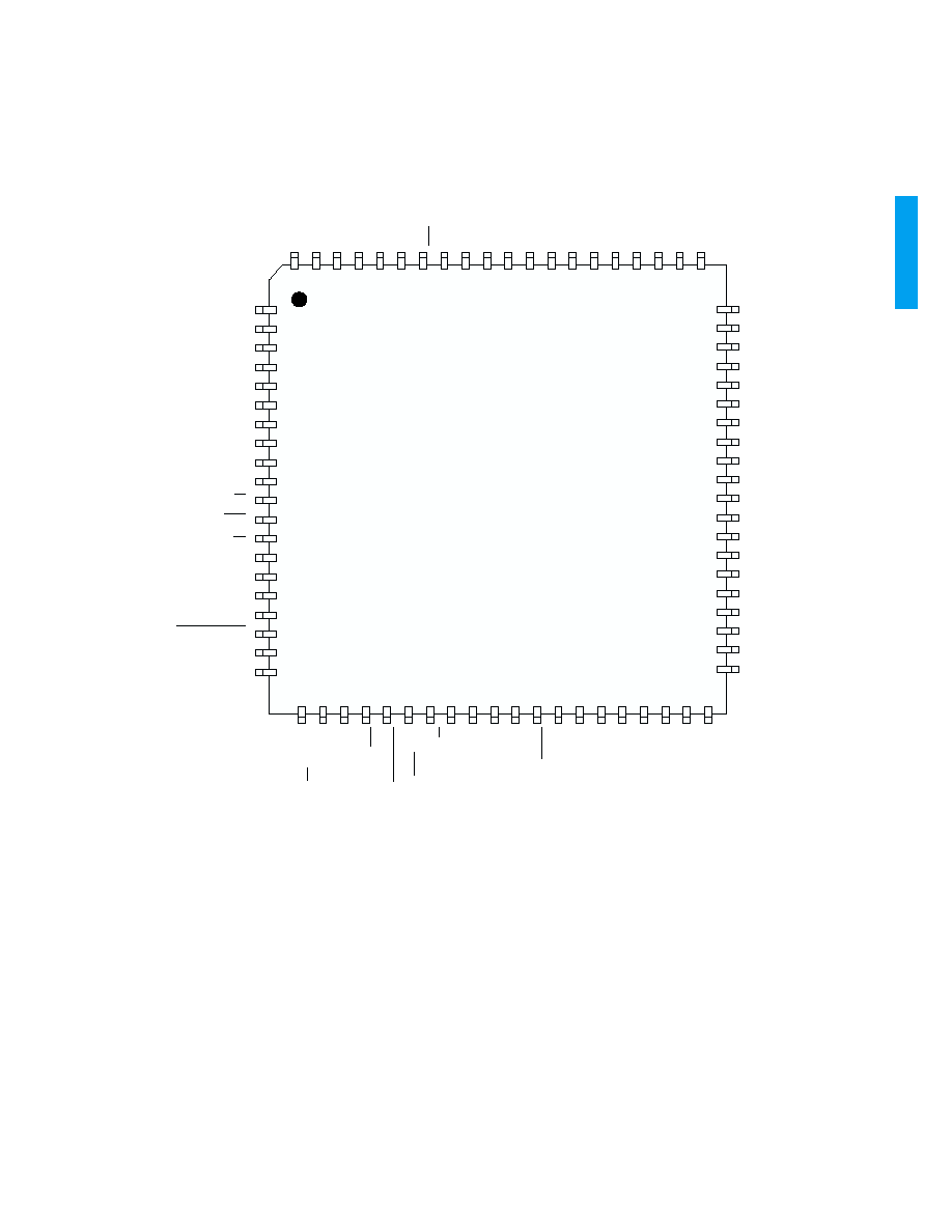
1. PIN OUT
1. PIN OUT
1. PIN OUT
1. PIN OUT
1.1 PIN ASSIGNMENT
GS1532
(Top View)
DVB_ASI
1
VCO_V
CC
CP_GND
VCO_GND
LF
VCO
LOCKED
CP_CAP
CORE_GND
CORE_V
DD
DIN19
DIN18
IO_V
DD
RSV2
RSV2
RSV2
RSV2
RSV1
RSV1
RSV1
RSV1
RSV1
RSV1
RSV1
RSV1
RSV1
RSV1
RSV2
PCLK
LB_CONT
VCO
DETECT_TRS
80
RESET_TRST
CD_GND
SDO
SDOUT_TDO
SDIN_TDI
SCLK_TCK
F
V
H
DIN0
DIN1
IO_GND
SDO
SDO_EN/DIS
BLANK
CORE_GND
CORE_V
DD
JT
AG/HOST
CS_TMS
21
60
CP_VDD
PD_VDD
PD_GND
SD/HD
20 bit/10 bit
SMPTE_BYPASS
CD_VDD
RSET
IOPROC_EN/DIS
DIN17
IO_VDD
DIN2
DIN3
DIN4
DIN5
DIN6
DIN7
DIN8
DIN9
IO_GND
IO_VDD
DIN10
DIN11
DIN12
DIN13
DIN14
DIN15
DIN16
IO_GND
GENNUM CORPORATION
21498 - 0
5
G
S
1
532
1.2 PIN DESCRIPTIONS
PIN
NUMBER
NAME
TIMING
TYPE
DESCRIPTION
1
CP_VDD
Analog
Input Power
Power supply connection for the charge pump 3.3V DC
2
PD_GND
Analog
Input Power
GND pin for the phase detector
3
PD_VDD
Analog
Input Power
Power supply for the Phase Detector 1.8V DC
9
DVB_ASI
Non
Synchronous
Input
CONTROL SIGNAL INPUT
Signal levels are LVCMOS / LVTTL compatible.
When set HIGH, the device will be configured for the transmission
of DVB-ASI data in SDTV mode, (SD/HD must be HIGH and
SMPTE_BYPASS must be LOW).
When set LOW, the device will not support the encoding of DVB-
ASI data.
11
SD/HD
Non
Synchronous
Input
CONTROL SIGNAL INPUT
Signal levels are LVCMOS / LVTTL compatible.
Used to select the current video rate as either 1.484 Gb/s HDTV or
270Mb/s SDTV. When SD/HD is HIGH, the mode is 270Mb/s.
The setting of this pin also determines the parallel input / output
clock rate and the slew rate of the cable driver output.
12
20bit/10bit
Non
Synchronous
Input
CONTROL SIGNAL INPUT
Signal levels are LVCMOS / LVTTL compatible.
Used to select the input bus width in SMPTE or Data-Through
modes.
13
IOPROC_EN/DIS
Non
Synchronous
Input
CONTROL SIGNAL INPUT
Signal levels are LVCMOS / LVTTL compatible.
Used to enable or disable I/O processing features
When IOPROC_EN/DIS is HIGH, the following I/O processing
features of the device are enabled.
∑
TRS insertion
∑
Line CRC insertion (HD-only)
∑
Line Number insertion (HD-only)
∑
Ancillary data checksum insertion
∑
EDH CRC insertion (SD-only)
∑
8b/10b encoding (DVB-ASI only)
To enable a subset of these features keep IOPROC_EN/DIS HIGH
and disable features in the host iterface.
When IOPROC_EN/DIS is LOW, the I/O processing features of the
device are disabled, regardless of whether the features are
enabled in the host interface.
GENNUM CORPORATION
21498 - 0
6
G
S
1
532
18
SMPTE_BYPASS
Non
Synchronous
Input
CONTROL SIGNAL INPUT
Signal levels are LVCMOS / LVTTL compatible.
Used to enable / disable all SMPTE encoding, scrambling and
word alignment.
When set LOW, SMPTE scrambling and encoding will be disabled.
When set HIGH, the device will carry out SMPTE scrambling /
coding. (DVB_ASI must be LOW)
19
RSET
Analog
Input
CONTROL SIGNAL INPUT
An external 1% resistor connected to this input is used to set the
SDO / SDO output signal amplitude.
20
CD_VDD
Analog
Input Power
Power supply for the serial digital cable driver 1.8V DC
21
SDO_EN/DIS
Non
Synchronous
Input
CONTROL SIGNAL INPUT
Signal levels are LVCMOS / LVTTL compatible.
Used to enable or disable the serial digital output stage.
When SDO_EN/DIS is LOW, the serial digital output signals SDO
and SDO are disabled and become high impedance.
When connected to logic HIGH, the serial digital output signals
SDO and SDO are enabled.
22
CD_GND
Analog
Input Power
GND connection - serial digital cable driver
23, 24
SDO, SDO
Analog
Output
SERIAL DATA OUTPUT SIGNAL
Serial digital output signal from the parallel to serial converter
operating at 1.485Gb/s, 1.485 /1.001Gb/s, or 270Mb/s.
The slew rate of the output is automatically controlled to meet
SMPTE 292M and 259M specifications according to the setting of
the SD/HD pin.
NOTE:
The SDO / SDO output signals will be forced to a logic LOW
level when the LOCKED pin = LOW.
1.2 PIN DESCRIPTIONS
(Continued)
(Continued)
(Continued)
(Continued)
PIN
NUMBER
NAME
TIMING
TYPE
DESCRIPTION
GENNUM CORPORATION
21498 - 0
7
G
S
1
532
25
RESET_TRST
Non
Synchronous
Input
CONTROL SIGNAL INPUT
Signal levels are LVCMOS / LVTTL compatible.
Used to reset the internal operating conditions to default settings
and to reset the JTAG test sequence.
Normal mode (JTAG/HOST = LOW)
When LOW, all functional blocks will be set to default conditions
and all input and output signals become high impedance including
the serial digital outputs SDO and SDO.
When HIGH, normal operation of the device resumes 10
µ
sec after
the low to high transition of the RESET_TRST signal.
JTAG test mode (JTAG/HOST = HIGH)
When LOW, all functional blocks will be set to default and the JTAG
test sequence will be held reset.
When HIGH, normal operation of the JTAG test sequence resumes.
26
JTAG/HOST
Non
Synchronous
Input
CONTROL SIGNAL INPUT
Signal levels are LVCMOS / LVTTL compatible.
Used to select JTAG Test Mode or Host Interface Mode.
When JTAG/HOST is HIGH, the CS_TMS, SDOUT_TDO, SDI_TDI
and SCLK_TCK pins are configured for JTAG test.
When JTAG/HOST is LOW, the above pins are configured for
normal host interface operation.
27
CS_TMS
Synchronous
with SCLK_TCK
Input
CONTROL SIGNAL INPUT
Signal levels are LVCMOS / LVTTL compatible.
Chip Select / Test Mode Select
When JTAG/HOST = HIGH, this pin is JTAG TMS.
When JTAG/HOST = LOW, this pin operates as the host interface
chip select and is active LOW.
28
SDOUT_TDO
Synchronous
with SCLK_TCK
Output
CONTROL SIGNAL OUTPUT
Signal levels are LVCMOS / LVTTL compatible.
Serial Data Output / Test Data Output
When JTAG/HOST = HIGH, this pin is JTAG TDO.
When JTAG/HOST = LOW, this pin is used to read status and
configuration data from the device.
1.2 PIN DESCRIPTIONS
(Continued)
(Continued)
(Continued)
(Continued)
PIN
NUMBER
NAME
TIMING
TYPE
DESCRIPTION

GENNUM CORPORATION
21498 - 0
8
G
S
1
532
29
SDIN_TDI
Synchronous
with SCLK_TCK
Input
CONTROL SIGNAL INPUT
Signal levels are LVCMOS / LVTTL compatible.
Serial Data In / Test Data In
When JTAG/HOST = HIGH, this pin is JTAG TDI
When JTAG/HOST = LOW, this pin is used to write address and
configuration data words into the device.
30
SCLK_TCK
Non
Synchronous
Input
CONTROL SIGNAL INPUT
Signal levels are LVCMOS / LVTTL compatible.
Serial Data Clock / Test Clock
When JTAG/HOST = HIGH, this pin is JTAG TCK
When JTAG/HOST = LOW, the host interface address and data is
shifted into / out of the device synchronously with this clock.
32
BLANK
Synchronous
with PCLK
Input
CONTROL SIGNAL INPUT
Signal levels are LVCMOS/LVTTL compatible.
When BLANK is LOW, the GS1532 sets the Luma and Chroma
input data to their appropriate blanking levels.
When BLANK is HIGH, the Luma and Chroma data pass through
this device unaltered.
33
CORE_GND
Non
Synchronous
Input Power
GND connection - Digital logic
34
F
Synchronous
with PCLK
Input
CONTROL SIGNAL INPUT
Signal levels are LVCMOS/LVTTL compatible.
The F signal is used to indicate the ODD/EVEN field of the video
signal.
The F signal will go HIGH for the entire period of field 2 as
indicated by the F bit in the received TRS signals.
The F signal will be LOW for all lines in field 1 and for all lines in
progressive scan systems.
The GS1532 uses the F input signal for internal timing generation
(when DETECT_TRS = LOW) and will set the F bit in all outgoing
TRS signals for the entire period that the F input signal is HIGH.
The F input is ignored when DETECT_TRS is HIGH.
1.2 PIN DESCRIPTIONS
(Continued)
(Continued)
(Continued)
(Continued)
PIN
NUMBER
NAME
TIMING
TYPE
DESCRIPTION
GENNUM CORPORATION
21498 - 0
9
G
S
1
532
35
V
Synchronous
with PCLK
Input
CONTROL SIGNAL INPUT
Signal levels are LVCMOS/LVTTL compatible.
The V signal is used to indicate the portion of the video field /
frame that is used for vertical blanking.
The V signal will be HIGH for the entire vertical blanking period.
The GS1532 uses the V input signal for internal timing generation
(when DETECT_TRS = LOW) and will set the V bit in all outgoing
TRS signals for the entire period that the V input signal is HIGH
(when IOPROC_EN/DIS is HIGH).
The V input is ignored when DETECT_TRS is HIGH.
36
H
Synchronous
with PCLK
Input
CONTROL SIGNAL INPUT
Signal levels are LVCMOS / LVTTL compatible.
The H signal is used to indicate the portion of the video line
containing active video data.
Active Line Blanking
By default, the H signal should be LOW for the active portion of the
video line. The signal goes LOW at the first active pixel of the line,
and then goes HIGH after the last active pixel of the line.
The H signal should remain HIGH throughout the horizontal
blanking period (including both SAV and EAV TRS).
TRS Based Blanking
The timing of this signal is programmable via the host interface
such that the H timing can be changed to be HIGH for the entire
horizontal blanking period as indicated by the H bit in the TRS
words.
The GS1532 uses the H input signal for internal timing generation
(when DETECT_TRS = LOW) and will use this signal in the
generation of the TRS signals (when IOPROC_EN/DIS is HIGH).
The H input is ignored when DETECT_TRS is HIGH.
37
CORE_VDD
Non
Synchronous
Input Power
Power connection - Digital logic 1.8V DC
1.2 PIN DESCRIPTIONS
(Continued)
(Continued)
(Continued)
(Continued)
PIN
NUMBER
NAME
TIMING
TYPE
DESCRIPTION

GENNUM CORPORATION
21498 - 0
10
G
S
1
532
38, 39,
42~48,
50
DIN[0:9]
Synchronous
with PCLK
Input
PARALLEL DATA BUS
Signal levels are LVCMOS / LVTTL compatible.
HDTV 20 bit mode
SD/HD = LOW
20 bit/10 bit = HIGH
Chroma data input in SMPTE mode
SMPTE_BYPASS = HIGH
Data input in data through mode
SMPTE_BYPASS = LOW
HDTV 10 bit mode
SD/HD = LOW
20 bit/10 bit = LOW
Must be connected to GND
SDTV 20 bit mode
SD/HD = HIGH
20 bit/10 bit = HIGH
Chroma data input in SMPTE mode
SMPTE_BYPASS = HIGH,
DVB_ASI = LOW
Data input in data through mode
SMPTE_BYPASS = LOW,
DVB_ASI = LOW
Must be connected to GND in DVB-ASI
mode
SMPTE_BYPASS = LOW,
DVB_ASI = HIGH
SDTV 10 bit mode
SD/HD = HIGH
20 bit/10 bit = LOW
Must be connected to GND
40, 49
IO_GND
Non
Synchronous
Input Power
GND connection - Digital I/O
41, 53
IO_VDD
Non
Synchronous
Input Power
Power connection - Digital I/O 3.3V DC.
1.2 PIN DESCRIPTIONS
(Continued)
(Continued)
(Continued)
(Continued)
PIN
NUMBER
NAME
TIMING
TYPE
DESCRIPTION
GENNUM CORPORATION
21498 - 0
11
G
S
1
532
51, 52,
54~59,
62, 63
DIN[10:19]
Synchronous
with PCLK
Input
PARALLEL DATA BUS
Signal levels are LVCMOS / LVTTL compatible.
HDTV 20 bit mode
SD/HD = LOW
20 bit/10 bit = HIGH
Luma data input in SMPTE mode
SMPTE_BYPASS = HIGH
Data input in data through mode
SMPTE_BYPASS = LOW
HDTV 10 bit mode
SD/HD= LOW
20 bit/10 bit = LOW
Multiplexed Luma and Chroma data input
in SMPTE mode
SMPTE_BYPASS = HIGH
Data input in data through mode
SMPTE_BYPASS = LOW
SDTV 20 bit mode
SD/HD = HIGH
20 bit/10 bit = HIGH
Luma data input in SMPTE mode
SMPTE_BYPASS = HIGH,
DVB_ASI = LOW
Data input in data through mode
SMPTE_BYPASS = LOW,
DVB_ASI = LOW
DVB-ASI data in DVB-ASI mode
SMPTE_BYPASS = LOW,
DVB_ASI = HIGH
SDTV 10 bit mode
SD/HD = HIGH
20 bit/10 bit = LOW
Multiplexed Luma and Chroma data input
in SMPTE mode
SMPTE_BYPASS = HIGH,
DVB_ASI = LOW
Data input in data through mode
SMPTE_BYPASS = LOW
DVB_ASI = LOW
DVB-ASI data in DVB-ASI mode
SMPTE_BYPASS = LOW,
DVB_ASI = HIGH
60
IO_GND
Non
Synchronous
Input Power
GND connection - Digital I/O
61
IO_VDD
Non
Synchronous
Input Power
Power connection - Digital I/O 3.3V DC.
64
CORE_VDD
Non
Synchronous
Input Power
Power connection - Digital logic 1.8V DC.
1.2 PIN DESCRIPTIONS
(Continued)
(Continued)
(Continued)
(Continued)
PIN
NUMBER
NAME
TIMING
TYPE
DESCRIPTION

GENNUM CORPORATION
21498 - 0
12
G
S
1
532
67
DETECT_TRS
Non
Synchronous
Input
CONTROL SIGNAL INPUT
Signal levels are LVCMOS / LVTTL compatible.
Used to select external HVF timing mode or TRS extraction timing
mode.
When DETECT_TRS is LOW, the device will extract all internal
timing information from the supplied H:V:F timing signals.
When DETECT TRS is HIGH, the device will extract all internal
timing information from TRS signals embedded in the supplied
video stream.
68
CORE_GND
Non
Synchronous
Input Power
GND connection - Digital logic
69
PCLK
Input
PARALLEL DATA BUS CLOCK
Signal levels are LVCMOS / LVTTL compatible.
HDTV 20 bit mode
PCLK = 74.25MHz (or 74.25/1.001MHz)
HDTV 10 bit mode
PCLK = 148. 5MHz (or 148.5/1.001MHz)
SDTV 20 bit mode
PCLK = 13.5MHz
SDTV 10 bit mode
PCLK = 27MHz
72
LOCKED
Synchronous
with PCLK
Output
STATUS SIGNAL Output
Signal levels are LVCMOS / LVTTL compatible.
This signal will be HIGH when the PLL has achieved lock to the
supplied PCLK signal.
This pin will be LOW under all other conditions.
When this signal is LOW, the serial digital output SDO / SDO will
be forced to a logic level LOW.
73,74
VCO, VCO
Analog
Input
Differential inputs for the external VCO. For single ended devices
such as the GO1525, VCO should be decoupled to GND.
75
VCO_GND
Analog
Output
Power
GND pin for the voltage controlled oscillator. (Internal regulator
output)
76
VCO_VCC
Analog
Output
Power
Power supply for the voltage controlled oscillator 2.5V DC supplied
by the device to the external VCO. (Internal regulator output).
77
LF
Analog
Output
Control voltage to external VCO.
78
CP_CAP
Analog
Input
PLL lock time constant capacitor connection.
79
LB_CONT
Analog
Input
CONTROL SIGNAL INPUT
Control voltage to set the loop bandwidth of the PLL.
80
CP_GND
Analog
Input Power
GND pin for the charge pump.
4, 5, 6, 7,
8, 10, 14,
15, 16, 17
RSV1
-
-
Reserved - connect to PD_GND.
31, 65,
66, 70,
71
RSV2
-
-
Reserved - connect to CORE_GND.
1.2 PIN DESCRIPTIONS
(Continued)
(Continued)
(Continued)
(Continued)
PIN
NUMBER
NAME
TIMING
TYPE
DESCRIPTION
GENNUM CORPORATION
21498 - 0
13
G
S
1
532
2. ELECTRICAL CHARACTERISTICS
2. ELECTRICAL CHARACTERISTICS
2. ELECTRICAL CHARACTERISTICS
2. ELECTRICAL CHARACTERISTICS
Fig. 1 Reflow Solder Profile
2.1 ABSOLUTE MAXIUMUM RATINGS
PARAMETER
VALUE/UNITS
Supply Voltage Core
-0.3V to +2.1V
Supply Voltage I/O
-0.3V to +4.6V
Input Voltage Range (any input)
-2.0V to + 5.25V
Ambient Operating Temperature
-20∞C < T
A
< 85∞C
Storage Temperature
-40∞C < T
STG
< 125∞C
Lead Temperature (soldering, 10 sec)
230∞C
NOTES:
1. See reflow profile solder
25∞C
100∞C
150∞C
183∞C
230∞C
220∞C
Time
Temperature
6 min. max
120 sec. max
60-150 sec.
10-20 sec.
3∞C/sec max
6∞C/sec max

GENNUM CORPORATION
21498 - 0
14
G
S
1
532
2.2 DC ELECTRICAL CHARACTERISTICS
V
DDCORE
= 1.8V, V
DDIO
= 3.3V T
A
= 0∞C to 70∞C, unless otherwise shown
PARAMETER
SYMBOL
CONDITIONS
MIN
TYP
MAX
UNITS
TEST
LEVEL
NOTES
Operating Temperature Range
T
A
0 25
70
∞C
1
Positive Core Supply Voltage
CORE_VDD
1.65
1.8
1.95
V
1
Positive I/O Supply Voltage
IO_VDD
3.0
3.3
3.6
V
1
Charge Pump Supply Voltage
CP_VDD
3.0
3.3
3.6
V
1
Phase Detector Supply Voltage
PD_VDD
1.65
1.8
1.95
V
1
External VCO Regulator Voltage
VCO_VCC
2.25
2.5
2.75
V
1
Cable Driver Supply Voltage
CD_VDD
1.71
1.8
1.89
V
1
Supply Current (Total)
V
DD
= Max, IO = Max,
T=70∞C
-
190
260
mA
2
Power (System Total)
P
D
(HD)
V
DD
= Max, IO = Max,
T=70∞C
-
460
570
mW
7
P
D
(SD)
V
DD
= Max, IO =
Max, T=70∞C
-
420
535
mW
7
Input Voltage LOW
V
IL
-
-
0.8
V
1
Input Voltage HIGH
V
IH
2.1
-
-
V
1
Output Voltage LOW
V
OL
-
0.2
0.4
V
1
Output Voltage HIGH
V
OH
V
DDIO
- 0.4
-
-
V
1
Output Common Mode
V
CM
75
load,
RSET=280
,
SD and
HD
0.8
1.0
1.2
V
1
RSET Voltage
V
RSET
RSET=280
0.54
0.6
0.66
mV
1
2
ESD Protection on all Pins
1
-
-
kV
3
TEST LEVELS
1. Production test at room temperature and nominal supply voltage with
guardbands for supply and temperature ranges.
2. Production test at room temperature and nominal supply voltage with
guardbands for supply and temperature ranges using correlated test.
3. Production test at room temperature and nominal supply voltage.
4. QA sample test.
5. Calculated result based on Level 1, 2, or 3.
6. Not tested. Guaranteed by design simulations.
7. Not tested. Based on characterization of nominal parts.
8. Not tested. Based on existing design/characterization data of similar
product.
9. Indirect test.
NOTES
1. All DC and AC electrical parameters within specification.
2. Set by value of RSET resistor.
3. MIL STD 883 ESD protection will be applied to all pins on the
device.

GENNUM CORPORATION
21498 - 0
15
G
S
1
532
2.3 AC ELECTRICAL CHARACTERISTICS
V
DDCORE
= 1.8V, V
DDIO
= 3.3V T
A
= 0∞C to 70∞C, unless otherwise shown
PARAMETER
SYMBOL
CONDITIONS
MIN
TYP
MAX
UNITS
TEST
LEVEL
NOTES
Serial Output Data Rate
DR
SDO
-
1.485,
1.485/1.001,
270
-
Gb/s
Gb/s
Mb/s
1
Serial Output RiseTime
20% ~ 80%
tr
SDO
No compensation for
return loss -
SMPTE 292M signal
-
150
230
ps
Return loss
compensation
recommended circuit
SMPTE 292M signal
-
200
260
ps
1
SMPTE 259M-C signal
400
550
1500
ps
1
Serial Output Fall Time
20% ~ 80%
tf
SDO
No compensation for
return loss -
SMPTE 292M signal
-
150
230
ps
Return loss
compensation
recommended circuit -
SMPTE 292M signal
-
235
260
ps
1
SMPTE 259M-C signal
400
550
1500
ps
1
Serial Output Intrinsic Jitter
t
IJ
Pseudo-random and
pathological HD signal
-
90
125
ps
1
t
IJ
Pseudo-random and
pathological SD signal
-
270
350
ps
1
Serial Output Duty Cycle
Distortion
HD
-
10
-
%
1
SD (270Mb/s)
-
20
-
%
1
Parallel Clock Frequency
f
PCLK
13.
5
- 148.
5
MHz
1
Parallel Clock Duty Cycle
40
50
60
%
3
Input Data Setup Time
t
SU
50% levels
1.5
-
-
ns
3
Input Data Hold Time
t
IH
50% levels
-
-
1.5
ns
3
GSPI Input Clock Frequency
f
GSPICLK
-
-
6.6
MHz
1
GSPI Input Clock Duty Cycle
DS
40
50
60
%
3
GSPI Data Setup Time
t
SUGSPI
0
-
-
ns
3
GSPI Data Hold Time
t
HOLDGSPI
-
-
1.43
ns
3
TEST LEVELS
1. Production test at room temperature and nominal supply voltage
with guardbands for supply and temperature ranges.
2. Production test at room temperature and nominal supply voltage
with guardbands for supply and temperature ranges using
correlated test.
3. Production test at room temperature and nominal supply voltage.
4. QA sample test.
5. Calculated result based on Level 1, 2, or 3.
6. Not tested. Guaranteed by design simulations.
7. Not tested. Based on characterization of nominal parts.
8. Not tested. Based on existing design/characterization data of similar
product.
9. Indirect test.

GENNUM CORPORATION
21498 - 0
16
G
S
1
532
2.4 INPUT/OUTPUT CIRCUITS
All resistors in ohms, all capacitors in farads, unless otherwise shown.
Fig. 2 Serial Digital Output
Fig. 4 VCO Control Output & PLL Lock Time Capacitor
Fig. 6 PCLK Input
Fig. 3 VCO Input
Fig. 5 PLL Loop Bandwidth Control
SDO
SDO
300
CP_CAP
LF
VDD
42K
63K
PCLK
VDD
25
25
VCO
VCO
5K
1.5K
800mV
8K
LB_CONT

GENNUM CORPORATION
21498 - 0
17
G
S
1
532
2.5 HOST INTERFACE
2.5 HOST INTERFACE
2.5 HOST INTERFACE
2.5 HOST INTERFACE
Table: 1 Host Interface Description
REGISTER NAME
NAME
DESCRIPTION
ADDRESS
BIT
R/W
DEFAULT
IOPROC_DISABLE
Not Used
000
15-9
H_CONFIG
Horizontal sync timing input configuration.
Set LOW when the H input timing is based
on active line blanking. Set HIGH when the
H input timing is based on the H bit of the
TRS words. See Figure 15.
8
Not Used
7
352M_INS
SMPTE352M packet insertion. In HD mode,
inserts the 352M packet in the Y channel
only when the four VIDEO_FORMAT
registers are programmed with non-zero
values and when IOPROC_EN/DIS is HIGH
and SMPTE_BYPASS is HIGH. This bit must
be set LOW.
6
R/W
0
ILLEGAL_REMAP
Illegal Code Re-mapping. Detection and
correction of illegal code words within the
active picture area (AP). Set HIGH to
disable. The IOPROC_EN/DIS pin and
SMPTE_BYPASS pin must be set HIGH.
5
R/W
0
(enabled)
EDH_CRC_INS
Error Detection & Handling (EDH) Cyclical
Redundancy Check (CRC) error correction.
In SD mode the GS1532 will generate and
insert EDH packets. Set HIGH to disable.
The IOPROC_EN/DIS pin and
SMPTE_BYPASS pin must be set HIGH.
4
R/W
0
(enabled)
ANC_CSUM_INS
Ancillary Data Check-sum insertion. Set
HIGH to disable. The IOPROC_EN/DIS pin
and SMPTE_BYPASS pin must be set HIGH.
3
R/W
0
(enabled)
CRC_INS
Y and C line based CRC insertion. In HD
mode, inserts line based CRC words in both
the Y and C channels. Set HIGH to disable
The IOPROC_EN/DIS pin and
SMPTE_BYPASS pin must be set HIGH.
2
R/W
0
(enabled)
LNUM_INS
Y and C line number insertion. In HD mode
set HIGH to disable. The IOPROC_EN/DIS
pin and SMPTE_BYPASS pin must be set
HIGH.
1
R/W
0
(enabled)
TRS_INS
Timing Reference Signal Insertion. Only
occurs when IOPROC_EN/DIS is HIGH and
SMPTE_BYPASS is HIGH. This bit must be
set LOW.
0
R/W
0
(disable)
Not Used
001
15-0

GENNUM CORPORATION
21498 - 0
18
G
S
1
532
Table 2: Host Interface Description
REGISTER
NAME
NAME
DESCRIPTION
ADDRESS
BIT
R/W
DEFAULT
EDH_FLAG
Not Used
002
15
ANC-UES
Ancillary Unknown Error Status will be
generated and inserted when IOPROC_EN/
DIS and SMPTE_BYPASS pins are HIGH and
EDH_CRC_INS bit is LOW. SD mode only.
14
R/W
ANC-IDA
Ancillary Internal device error Detected
Already will be generated and inserted when
IOPROC_EN/DIS and SMPTE_BYPASS pins
are HIGH and EDH_CRC_INS bit is LOW. SD
mode only.
13
R/W
ANC-IDH
Ancillary Internal device error Detected Here
will be generated and inserted when
IOPROC_EN//DIS and SMPTE_BYPASS pins
are HIGH and EDH_CRC_INS bit is LOW. SD
mode only.
12
R/W
ANC-EDA
Ancillary Error Detected Already will be
generated and inserted when IOPROC_EN/
DIS and SMPTE_BYPASS pins are HIGH and
EDH_CRC_INS bit is LOW. SD mode only.
11
R/W
ANC-EDH
Ancillary Error Detected Here will be
generated and inserted when IOPROC_EN//
DIS and SMPTE_BYPASS pins are HIGH and
EDH_CRC_INS bit is LOW. SD mode only.
10
R/W
FF-UES
Full Field Unknown Error will be generated
and inserted when IOPROC_EN/DIS and
SMPTE_BYPASS pins are HIGH and
EDH_CRC_INS bit is LOW. SD mode only.
9
R/W
FF-IDA
Full Field Internal device error Detected
Already will be generated and inserted when
IOPROC_EN/DIS and SMPTE_BYPASS pins
are HIGH and EDH_CRC_INS bit is LOW. SD
mode only.
8
R/W
FF-IDH
Full Field Internal device error Detected will
be generated and inserted when
IOPROC_EN/DIS and SMPTE_BYPASS pins
are HIGH and EDH_CRC_INS bit is LOW. SD
mode only.
7
R/W
FF-EDA
Full Field Error Detected Already will be
generated and inserted when IOPROC_EN/
DIS and SMPTE_BYPASS pins are HIGH and
EDH_CRC_INS bit is LOW. SD mode only.
6
R/W
FF-EDH
Full Field Error Detected Here will be
generated and inserted when IOPROC_EN/
DIS and SMPTE_BYPASS pins are HIGH and
EDH_CRC_INS bit is LOW. SD mode only.
5
R/W

GENNUM CORPORATION
21498 - 0
19
G
S
1
532
EDH_FLAG
AP-UES
Active Picture Unknown Error Status will be
generated and inserted when IOPROC_EN/
DIS and SMPTE_BYPASS pins are HIGH and
EDH_CRC_INS bit is LOW. SD mode only.
002
4
R/W
AP-IDA
Active Picture Internal device error Detected
Already will be generated and inserted when
IOPROC_EN/DIS and SMPTE_BYPASS pins are
HIGH and EDH_CRC_INS bit is LOW. SD mode
only.
3
R/W
AP-IDH
Active Picture Internal device error Detected
Here will be generated and inserted when
IOPROC_EN/DIS and SMPTE_BYPASS pins
are HIGH and EDH_CRC_INS bit is LOW. SD
mode only.
2
R/W
AP-EDA
Active Picture Error Detected Already will be
generated and inserted when IOPROC_EN/
DIS and SMPTE_BYPASS pins are HIGH and
EDH_CRC_INS bit is LOW. SD mode only.
1
R/W
AP-EDH
Active Picture Error Detected Here will be
generated and inserted when IOPROC_EN/
DIS and SMPTE_BYPASS pins are HIGH and
EDH_CRC_INS bit is LOW. SD mode only.
0
R/W
Table 3: Host Interface Description
REGISTER NAME
NAME
DESCRIPTION
ADDRESS
BIT
R/W
DEFAULT
Not Used
003
15-0
VIDEO_STANDARD
Not Used
004
15
VD_STD[4:0]
Video Data Standard
(see Table 7)
14-10
R
0
INT_PROG
Interlace/Progressive: Set LOW if
detected video standard is
PROGRESSIVE and is set HIGH if it
is INTERLACED.
9
R
0
STD_LOCK
Standard Lock: Set HIGH when
flywheel has achieved full
synchronization.
8
R
0
Not Used
7-0
Table 2: Host Interface Description (Continued)
REGISTER
NAME
NAME
DESCRIPTION
ADDRESS
BIT
R/W
DEFAULT
GENNUM CORPORATION
21498 - 0
20
G
S
1
532
Table 4: Host Interface Description
REGISTER NAME
NAME
DESCRIPTION
ADDRESS
BIT
R/W
DEFAULT
Not Used
005
15-0
Not Used
006
15-0
Not Used
007
15-0
Not Used
008
15-0
Not Used
009
15-0
VIDEO_FORMAT
SMPTE 352M Byte 2
SMPTE 352M Byte 2 information
must be programmed in this
register when 352M_INS = LOW
010
15-8
R/W
0
SMPTE 352M Byte 1
SMPTE 352M Byte 1 information
must be programmed in this
register when 352M_INS = LOW
7-0
R/W
0
SMPTE 352M Byte 4
SMPTE 352M Byte 4 information
must be programmed in this
register when 352M_INS = LOW
011
15-8
R/W
0
SMPTE 352M Byte 3
SMPTE 352M Byte 3 information
must be programmed in this
register when 352M_INS = LOW
7-0
R/W
0
Not Used
012
15-0
Not Used
013
15-0
Table 5: Host Interface Description
REGISTER NAME
NAME
DESCRIPTION
ADDRESS
BIT
R/W
DEFAULT
RASTER_STRUCTURE
Not Used
014
15-12
RASTER_STRUCTURE_1
[11:0]
Words Per Active Line
11-0
R
0
Not Used
015
15-12
RASTER_STRUCTURE_2
[11:0]
Words Per Total Line.
11-0
R
0
Not Used
016
15-11
RASTER_STRUCTURE_3
[10:0]
Total Lines Per Frame
10-0
R
0
Not Used
017
15-11
RASTER_STRUCTURE_4
[10:0]
Active Lines Per Field
10-0
R
0

GENNUM CORPORATION
21498 - 0
21
G
S
1
532
Table 6: Host Interface Description
REGISTER NAME
NAME
DESCRIPTION
ADDRESS
BIT
R/W
DEFAULT
AP_LINE_START_F0
Not Used
018
15-10
AP_LINE_START_F0
[9:0]
Field 0 Active Picture start line data
used to set EDH calculation range
outside of RP 165 values.
9-0
R/W
0
AP_LINE_END_F0
Not Used
019
15-10
AP_LINE_END_F0
[9:0]
Field 0 Active Picture end line data
used to set EDH calculation range
outside of RP 165 values.
9-0
R/W
0
AP_LINE_START_F1
Not Used
020
15-10
AP_LINE_START_F1
[9:0]
Field 1 Active Picture start line data
used to set EDH calculation range
outside of RP 165 values.
9-0
R/W
0
AP_LINE_END_F1
Not Used
021
15-10
AP_LINE_END_F1
[9:0]
Field 1 Active Picture end line data
used to set EDH calculation range
outside of RP 165 values.
9-0
R/W
0
FF_LINE_START_F0
Not Used
022
15-10
FF_LINE_START_F0
[9:0]
Field 0 Full Field start line data used to
set EDH calculation range outside of RP
165 values.
9-0
R/W
0
FF_LINE_END_F0
Not Used
023
15-10
FF_LINE_END_F0
[9:0]
Field 0 Full Field end line data used to
set EDH calculation range outside of RP
165 values.
9-0
R/W
0
FF_LINE_START_F1
Not Used
024
15-10
FF_LINE_START_F1
[9:0]
Field 1 Full Field start line data used to
set EDH calculation range outside of
RP-165 values.
9-0
R/W
0
FF_LINE_END_F1
Not Used
025
15-10
FF_LINE_END_F1
Field 1 Full Field end line data used to
set EDH calculation range outside of
RP-165 values.
9-0
R/W
0
Not Used
026
15-0
LINE_0_352M
Not Used
027
15-11
LINE_0_352M[10:0]
Data bit 10 of first line where
SMPTE352M packet is inserted. This
line number overrides the standard line
number.
10-0
R/W
0
LINE_1_352M
Not Used
028
15-11
LINE_1_352M[10:0]
Second line where SMPTE352M packet
is inserted. This line number overrides
the standard line number.
10-0
R/W
0
GENNUM CORPORATION
21498 - 0
22
G
S
1
532
Table 7: Supported Video Standards (VD_STD)
SMPTE
STANDARD
ACTIVE VIDEO AREA
LENGTH OF
HANC
LENGTH OF
ACTIVE VIDEO
TOTAL
SAMPLES
SMPTE 352M
LINES
VD_STD[4:0]
260M (HD)
1920x1035/60 (2:1)
268
1920
2200
10, 572
15h
295M (HD)
1920x1080/50 (2:1)
444
1920
2376
10, 572
14h
274M (HD)
1920x1080/60 (2:1) or
1920x1080/30 (PsF)
268
1920
2200
10, 572
0Ah
1920x1080/50 (2:1) or
1920x1080/25 (PsF)
708
1920
2640
10, 572
0Ch
1920x1080/30 (1:1)
268
1920
2200
18
0Bh
1920x1080/25 (1:1)
708
1920
2640
18
0Dh
1920x1080/24 (1:1)
818
1920
2750
18
10h
1920x1080/24 (PsF)
818
1920
2750
10, 572
11h
1920x1080/25 (1:1) - EM
324
2304
2640
18
0Eh
1920x1080/25 (PsF) - EM
324
2304
2640
10, 572
0Fh
1920x1080/24 (1:1) - EM
338
2400
2750
18
12h
1920x1080/24 (PsF) - EM
338
2400
2750
10, 572
13h
296M (HD)
1280x720/30 (1:1)
2008
1280
3300
13
02h
1280x720/30 (1:1) - EM
408
2880
3300
13
03h
1280x720/50 (1:1)
688
1280
1980
13
04h
1280x720/50 (1:1) - EM
240
1728
1980
13
05h
1280x720/25 (1:1)
2668
1280
3960
13
06h
1280x720/25 (1:1) - EM
492
3456
3960
13
07h
1280x720/24 (1:1)
2833
1280
4125
13
08h
1280x720/24 (1:1) - EM
513
3600
4125
13
09h
1280x720/60 (1:1)
358
1280
1650
13
00h
1280x720/60 (1:1) - EM
198
1440
1650
13
01h
125M (SD)
1440x487/60 (2:1)(Or dual
link progressive)
268
1440
1716
3, 276
16h
1440x507/60 (2:1)
268
1440
1716
3, 276
17h
525-line 487 generic
-
-
1716
3, 276
19h
525-line 507 generic
-
-
1716
3, 276
1Bh
ITU-R BT.656
(SD)
1440x576/50 (2:1)
268
1440
1716
3, 276
18h
625-line generic (EM)
-
-
1728
9, 322
1Ah
Unknown HD
SD/HD = 0
-
-
-
-
1Dh
Unknown SD
SD/HD = 1
-
-
-
-
1Eh
Reserved
1Ch, 1Fh
GENNUM CORPORATION
21498 - 0
23
G
S
1
532
H
H
H
HO
O
O
OS
S
S
ST
T
T
T
I
II
IN
N
N
NT
T
T
TE
E
E
ER
R
R
RF
F
F
FA
A
A
AC
C
C
CE
E
E
E
M
M
M
MA
A
A
AP
P
P
P
HOST Name
Address
15
14
13
12
11
10
9
8
7
6
5
4
3
2
1
0
Line 1 352M[10:0]
28
Not Used
Not Used
Not Used
Not Used
Not Used
b10
b9
b8
b7
b6
b5
b4
b3
b2
b1
b0
Line 0 352M[10:0]
27
Not Used
Not Used
Not Used
Not Used
Not Used
b10
b9
b8
b7
b6
b5
b4
b3
b2
b1
b0
26
Not Used
Not Used
Not Used
Not Used
Not Used
Not Used
Not Used
Not Used
Not Used
Not Used
Not Used
Not Used
Not Used
Not Used
Not Used
Not Use
d
FF_LINE_END_F1[9:0]
25
Not Used
Not Used
Not Used
Not Used
Not Used
Not Used
b9
b8
b7
b6
b5
b4
b3
b2
b1
b0
FF_LINE_START_F1[9:0]
24
Not Used
Not Used
Not Used
Not Used
Not Used
Not Used
b9
b8
b7
b6
b5
b4
b3
b2
b1
b0
FF_LINE_END_F0[9:0]
23
Not Used
Not Used
Not Used
Not Used
Not Used
Not Used
b9
b8
b7
b6
b5
b4
b3
b2
b1
b0
FF_LINE_START_F0[9:0]
22
Not Used
Not Used
Not Used
Not Used
Not Used
Not Used
b9
b8
b7
b6
b5
b4
b3
b2
b1
b0
AP_LINE_END_F1[9:0]
21
Not Used
Not Used
Not Used
Not Used
Not Used
Not Used
b9
b8
b7
b6
b5
b4
b3
b2
b1
b0
AP_LINE_START_F1[9:0]
20
Not Used
Not Used
Not Used
Not Used
Not Used
Not Used
b9
b8
b7
b6
b5
b4
b3
b2
b1
b0
AP_LINE_END_F0[9:0]
19
Not Used
Not Used
Not Used
Not Used
Not Used
Not Used
b9
b8
b7
b6
b5
b4
b3
b2
b1
b0
AP_LINE_START_F0[9:0]
18
Not Used
Not Used
Not Used
Not Used
Not Used
Not Used
b9
b8
b7
b6
b5
b4
b3
b2
b1
b0
RASTER_STRUCTURE _4[10:0]
17
Not Used
Not Used
Not Used
Not Used
Not Used
b10
b9
b8
b7
b6
b5
b4
b3
b2
b1
b0
RASTER_STRUCTURE _3[10:0]
16
Not Used
Not Used
Not Used
Not Used
Not Used
b10
b9
b8
b7
b6
b5
b4
b3
b2
b1
b0
RASTER_STRUCTURE _2[11:0]
15
Not Used
Not Used
Not Used
Not Used
b11
b10
b9
b8
b7
b6
b5
b4
b3
b2
b1
b0
RASTER_STRUCTURE _1[11:0]
14
Not Used
Not Used
Not Used
Not Used
b11
b10
b9
b8
b7
b6
b5
b4
b3
b2
b1
b0
RESERVED
13
Not Used
Not Used
Not Used
Not Used
Not Used
Not Used
Not Used
Not Used
Not Used
Not Used
Not Used
Not Used
Not Used
Not Used
Not Used
Not Use
d
RESERVED
12
Not Used
Not Used
Not Used
Not Used
Not Used
Not Used
Not Used
Not Used
Not Used
Not Used
Not Used
Not Used
Not Used
Not Used
Not Used
Not Use
d
VIDEO_FORMAT(4,3)[[7:0][7:0]
11
VF4-b7
VF4-b6
VF4-b5
VF4-b4
VF4-b3
VF4-b2
VF4-b1
VF4-b0
VF3-b7
VF3-b6
VF3-b5
VF3-b4
VF3-b3
VF3-b2
VF3-b1
VF3-b0
VIDEO_FORMAT(2,1)[[7:0][7:0]
10
VF2-b7
VF2-b6
VF2-b5
VF2-b4
VF2-b3
VF2-b2
VF2-b1
VF2-b0
VF1-b7
VF1-b6
VF1-b5
VF1-b4
VF1-b3
VF1-b2
VF1-b1
VF1-b0
9
Not Used
Not Used
Not Used
Not Used
Not Used
Not Used
Not Used
Not Used
Not Used
Not Used
Not Used
Not Used
Not Used
Not Used
Not Used
Not Use
d
8
Not Used
Not Used
Not Used
Not Used
Not Used
Not Used
Not Used
Not Used
Not Used
Not Used
Not Used
Not Used
Not Used
Not Used
Not Used
Not Use
d
7
Not Used
Not Used
Not Used
Not Used
Not Used
Not Used
Not Used
Not Used
Not Used
Not Used
Not Used
Not Used
Not Used
Not Used
Not Used
Not Use
d
6
Not Used
Not Used
Not Used
Not Used
Not Used
Not Used
Not Used
Not Used
Not Used
Not Used
Not Used
Not Used
Not Used
Not Used
Not Used
Not Use
d
5
Not Used
Not Used
Not Used
Not Used
Not Used
Not Used
Not Used
Not Used
Not Used
Not Used
Not Used
Not Used
Not Used
Not Used
Not Used
Not Use
d
VIDEO_STANDARD
4
Not Used
VDS-b4
VDS-b3
VDS-b2
VDS-b1
VDS-b0
Not Used
STD_LOCK
Not Used
Not Used
Not Used
Not Used
Not Used
Not Used
Not Used
Not Used
3
Not Used
Not Used
Not Used
Not Used
Not Used
Not Used
Not Used
Not Used
Not Used
Not Used
Not Used
Not Used
Not Used
Not Used
Not Used
Not Use
d
EDH_FLAG_REGISTER
2
Not Used
ANC-UES
ANC-IDA
ANC-IDH
ANC-EDA
ANC-EDH
FF-UES
FF-IDA
FF-IDH
FF-EDA
FF-EDH
AP-UES
AP-IDA
AP-IDH
AP-EDA
AP-EDH
1
Not Used
Not Used
Not Used
Not Used
Not Used
Not Used
Not Used
Not Used
Not Used
Not Used
Not Used
Not Used
Not Used
Not Used
Not Used
Not Use
d
I/O PROCESSING
0
Not Used
Not Used
Not Used
Not Used
Not Used
Not Used
Not Used
Not Used
352M
_INS
ILLEGAL
_REMAP
EDH_CRC
_INS
ANC_CSUM
_INS
Not Used
Not Used
TRS
_INS
H_CONFIG

GENNUM CORPORATION
21498 - 0
24
G
S
1
532
H
H
H
HO
O
O
OS
S
S
ST
T
T
T
I
II
IN
N
N
NT
T
T
TE
E
E
ER
R
R
RF
F
F
FA
A
A
AC
C
C
CE
E
E
E
M
M
M
MA
A
A
AP
P
P
P
(
(
(
(R
R
R
RE
E
E
EA
A
A
AD
D
D
D
O
O
O
ON
N
N
NL
L
L
LY
Y
Y
Y
R
R
R
RE
E
E
EG
G
G
GI
II
IS
S
S
ST
T
T
TE
E
E
ER
R
R
RS
S
S
S)
)
)
)
HOST Table Name
Address
15
14
13
12
11
10
9
8
7
6
5
4
3
2
1
0
28
27
26
25
24
23
22
21
20
19
18
RASTER_STRUCTURE _4[10:0]
17
b10
b9
b8
b7
b6
b5
b4
b3
b2
b1
b0
RASTER_STRUCTURE _3[10:0]
16
b10
b9
b8
b7
b6
b5
b4
b3
b2
b1
b0
RASTER_STRUCTURE _2[11:0]
15
b11
b10
b9
b8
b7
b6
b5
b4
b3
b2
b1
b0
RASTER_STRUCTURE _1[11:0]
14
b11
b10
b9
b8
b7
b6
b5
b4
b3
b2
b1
b0
13
12
11
10
9
8
7
6
5
VIDEO_STANDARD
4
VDS-b4
VDS-b3
VDS-b2
VDS-b1
VDS-b0
STD_LOCK
3
2
1
0
GENNUM CORPORATION
21498 - 0
25
G
S
1
532
H
H
H
HO
O
O
OS
S
S
ST
T
T
T
I
II
IN
N
N
NT
T
T
TE
E
E
ER
R
R
RF
F
F
FA
A
A
AC
C
C
CE
E
E
E
M
M
M
MA
A
A
AP
P
P
P
(
(
(
(R
R
R
R/
/
/
/W
W
W
W
C
C
C
CO
O
O
ON
N
N
NF
F
F
FI
II
IG
G
G
GU
U
U
UR
R
R
RA
A
A
AB
B
B
BL
L
L
LE
E
E
E
R
R
R
RE
E
E
EG
G
G
GI
II
IS
S
S
ST
T
T
TE
E
E
ER
R
R
RS
S
S
S)
)
)
)
HOST Table Name
Address
15
14
13
12
11
10
9
8
7
6
5
4
3
2
1
0
Line 1 352M[10:0]
28
b10
b9
b8
b7
b6
b5
b4
b3
b2
b1
b0
Line 0 352M[10:0]
27
b10
b9
b8
b7
b6
b5
b4
b3
b2
b1
b0
26
FF_LINE_END_F1[10:0]
25
b9
b8
b7
b6
b5
b4
b3
b2
b1
b0
FF_LINE_START_F1[10:0]
24
b9
b8
b7
b6
b5
b4
b3
b2
b1
b0
FF_LINE_END_F0[10:0]
23
b9
b8
b7
b6
b5
b4
b3
b2
b1
b0
FF_LINE_START_F0[10:0]
22
b9
b8
b7
b6
b5
b4
b3
b2
b1
b0
AP_LINE_END_F1[10:0]
21
b9
b8
b7
b6
b5
b4
b3
b2
b1
b0
AP_LINE_START_F1[10:0]
20
b9
b8
b7
b6
b5
b4
b3
b2
b1
b0
AP_LINE_END_F0[10:0]
19
b9
b8
b7
b6
b5
b4
b3
b2
b1
b0
AP_LINE_START_F0[10:0]
18
b9
b8
b7
b6
b5
b4
b3
b2
b1
b0
17
16
15
14
13
12
VIDEO_FORMAT(4,3)[[7:0][7:0]
11
VF4-b7
VF4-b6
VF4-b5
VF4-b4
VF4-b3
VF4-b2
VF4-b1
VF4-b0
VF3-b7
VF3-b6
VF3-b5
VF3-b4
VF3-b3
VF3-b2
VF3-b1
VF3-b0
VIDEO_FORMAT(2,1)[[7:0][7:0]
10
VF2-b7
VF2-b6
VF2-b5
VF2-b4
VF2-b3
VF2-b2
VF2-b1
VF2-b0
VF1-b7
VF1-b6
VF1-b5
VF1-b4
VF1-b3
VF1-b2
VF1-b1
VF1-b0
9
8
7
6
5
4
3
EDH_FLAG_REGISTER
2
ANC-UES
ANC-IDA
ANC-IDH
ANC-EDA
ANC-EDH
FF-UES
FF-IDA
FF-IDH
FF-EDA
FF-EDH
AP-UES
AP-IDA
AP-IDH
AP-EDA
AP-EDH
1
IOPROC_DISABLE_REGISTER
0
H_CONFIG
352M
_INS
ILLEGAL
_REMAP
EDH_CRC
_INS
ANC_CSUM
_INS
TRS
_INS

GENNUM CORPORATION
21498 - 0
26
G
S
1
532
3. DETAILED DESCRIPTION
3. DETAILED DESCRIPTION
3. DETAILED DESCRIPTION
3. DETAILED DESCRIPTION
3.1 GSPI - APPLICATION LAYER HOST INTERFACE
The GSPI, or Gennum Serial Peripheral Interface is a 4-wire
interface provided to allow the application layer to access
additional status information through configuration registers
in the GS1532.
The GSPI comprises a serial data input signal SDIN, serial
data output signal SDOUT, an active low chip select CS,
and a burst clock SCLK.
Because these pins are shared with the JTAG interface
port, an additional control signal pin JTAG/HOST is
provided.
When JTAG/HOST is LOW, the GSPI interface is enabled.
When JTAG/HOST is HIGH, the JTAG interface is enabled.
When operating in GSPI mode, the SCLK, SDIN, and CS
signals are provided by the application interface. The
SDOUT pin is a high-impedance output allowing multiple
devices to be connected. The interface is illustrated in the
Figure 7.
All read or write access to the GS1532 is initiated and
terminated by the application host processor. Each access
always begins with a command / address word followed by
a data read or write to/from the GS1532.
Fig. 7 GSPI Application Interface Connection
3.1.1 Command Word Description
The command word consists of a 16-bit word transmitted
MSB first and contains a read/write bit, nine reserved bits
and a 6-bit address.
Command words are clocked into the deserializer on the
rising edge of the serial clock SCLK, which operates in a
burst fashion. The chip select CS signal must be active low
for at least 1.5ns (t
0
in Figure 10) before the first clock edge
to ensure proper operation.
R/W: Read command if R/W='1', write command if R/W='0'.
RSV: Reserved for additional functionality
[A5:A0]: Address
Each command word must be followed by only one data
word to ensure proper operation.
3.1.2 Data Read or Write Access
Serial data is transmitted or received MSB first synchronous
with the rising edge of the serial clock SCLK. The chip
select CS signal must be active low for at least 1.5ns (t
0
in
Figure 10) before the first clock edge to ensure proper
operation. The first bit (MSB) of the serial output SDOUT is
available 12ns (t
4
in Figure 11) following the last falling
SCLK edge of the read command word, the remaining bits
are clocked out on the negative edges of SCLK. Figures 10
and 11 illustrate the interface timing.
The device will not drive any signal out during the power up
phase or when the external RESET_TRST pin is asserted
LOW.
Fig. 8 Command Word Format
Fig. 9 Data Word Format
SCLCK
CS
SDOUT
SDIN
SCLCK
CS
SDIN
SDOUT
Application Host
GS1532
R/W
RSV
RSV
RSV
A0
A1
A2
A3
A4
A5
RSV
RSV
RSV
RSV
RSV
RSV
MSB
LSB
D15
D14
D13
D12
D0
D1
D2
D3
D4
D5
D6
D7
D8
D9
D11
D10
MSB
LSB

GENNUM CORPORATION
21498 - 0
27
G
S
1
532
3.1.3 GSPI Timing
Write and read mode timing for the GSPI interface is as
shown in the following diagrams.
Fig. 10 Write Mode
Fig. 11 Read Mode
3.1.4 Configuration and Status Register Description
The GS1532 provides status and configuration registers.
These registers may be used to enable additional features
of the device and/or to provide additional status
information.
The GS1532 contains the following registers:
∑
4 VIDEO_FORMAT registers
∑
4 RASTER_STRUCTURE registers
∑
1 EDH_CALCULATION_RANGE register
∑
2 DATA_FORMAT registers
∑
1 IOPROC_DISABLE_MASK register
All of these registers are available to the application layer
via the host interface and are all individually addressable.
Where status registers contain less than the full 16 bits of
information however, two or more registers may be
combined at a single logical address.
3.2 JTAG TEST
When the JTAG/HOST is HIGH, the host interface port will
be configured for JTAG test operation. In this mode the
SCLK, SDIN, SDOUT and CS become TCK, TDI, TDO and
TMS. In addition, the TRST pin become active.
Boundary scan testing using the JTAG interface will be
enabled in this mode.
There are two methods in which JTAG can be used on the
GS1532:
(1) as a stand-alone JTAG interface to be used at in-circuit
ATE (Automatic Test Equipment) during PCB assembly,
or
(2) under control of the host for applications such as system
power on self tests.
When the JTAG tests are applied by ATE, care must be
taken to disable any other devices driving the pins. If the
tests are to be applied only at ATE, this can be
accomplished with tri-state buffers used in conjunction with
the JTAG/HOST signal. This is shown in Figure 12.
Fig. 12 In-Circuit JTAG
R/W
RSV
RSV
A0
A1
A2
A3
A4
A5
RSV
RSV
RSV
RSV
RSV
RSV
D15
D14
D13
D12
D0
D1
D2
D3
D4
D5
D6
D7
D8
D9
D11
D10
SCLK
CS
SDIN
SDOUT
t
0
t
3
t
1
t
2
RSV
R/W
RSV
RSV
A0
A1
A2
A3
A4
A5
RSV
RSV
RSV
RSV
RSV
RSV
D15
D14
D13
D12
D0
D1
D2
D3
D4
D5
D6
D7
D8
D9
D11
D10
SCLK
CS
SDIN
SDOUT
t
4
t
5
RSV
Application HOST
GS1532
CS_TMS
SCLK_TCK
SDIN_TDI
SDOUT_TDO
JTAG_HOST
In-circuit ATE probe

GENNUM CORPORATION
21498 - 0
28
G
S
1
532
Alternatively, if the test capabilities are to be used in the
system, the host may still control the JTAG/HOST signal, but
some means for tri-stating the host must exist in order to
use the interface at ATE. This is represented in Figure 13.
Fig. 13 System JTAG
3.3 PARALLEL DATA INPUTS DIN[19:10] AND DIN[9:0]
Data outputs leave the device on the rising edge of PCLK
as shown in Figure 14.
The data may be scrambled or unscrambled, framed or
unframed and may be presented in 20-bit or 10-bit format.
The output data format is defined by the setting of external
pins 20bit/10bit, SMPTE_BYPASS and DVB_ASI.
Table 8 lists the output signal formats according to the
external selection pins for the GS1560. It should be noted
that DVB-ASI output will always be in 10-bit format,
regardless of the setting of the 20bit/10bit pin.
Fig. 14 PCLK to Data and Control Signal Input Timing
3.3.1 Input Data Format in SMPTE Mode
When the device is operating in SMPTE mode
(SMPTE_BYPASS = HIGH), data is presented to the input
bus in either multiplexed or demultiplexed form depending
on the setting of the 20bit/10bit pin.
When operating in 20-bit mode (20bit/10bit = HIGH), the
input data format will be (word aligned), demultiplexed
Luma and Chroma data.
Application HOST
GS1532
CS_TMS
SCLK_TCK
SDIN_TDI
SDOUT_TDO
JTAG_HOST
In-circuit ATE probe
Tri-State
PCLK
DIN[19:0]
DATA
DATA
t
OH
t
OD
Control signal
input/output
Table 8: Input Data Format Selections
OUTPUT Data Format
Pin Settings
DIN[9:0]
DIN[19:10]
20bit/10bit
SD/HD
SMPTE_BYPASS
DVB_ASI
20-bit demultiplexed HD format
HIGH
LOW
HIGH
Don't Care
Chroma
Luma
20-bit data Input HD format
HIGH
LOW
LOW
Don't Care
DATA
DATA
20-bit demultiplexed SD format
HIGH
HIGH
HIGH
LOW
Chroma
Luma
20-bit data input SD format
HIGH
HIGH
LOW
LOW
DATA
DATA
20-bit ASI input SD format
HIGH
HIGH
LOW
HIGH
High
Impedance
DVB-ASI data
10-bit multiplexed HD format
LOW
LOW
HIGH
Don't Care
High
Impedance
Luma/Chroma
10-bit data input HD format
LOW
LOW
LOW
Don't Care
High
Impedance
DATA
10-bit multiplexed SD format
LOW
HIGH
HIGH
LOW
High
Impedance
Luma/Chroma
10-bit data input SD format
LOW
HIGH
LOW
LOW
High
Impedance
DATA
10-bit ASI input SD format
LOW
HIGH
LOW
HIGH
High
Impedance
DVB-ASI data
For all data input format cases DIN[19] represents the most significant bit of the input data.

GENNUM CORPORATION
21498 - 0
29
G
S
1
532
When operating in 10-bit mode (20bit/10bit = LOW), the
input data format will be (word aligned), multiplexed Luma
and Chroma data. In this mode, the data will be presented
on the DIN[19:10] pins, with DIN[9:0] being high
impedance.
3.3.2 Input Data Format in Data Through Mode
Data through mode is enabled when both the
SMPTE_BYPASS and DVB_ASI pins are LOW.
In this mode data at the input bus is passed to the serial
output without any coding, scrambling or word-alignment
taking place. The input data width is controlled by the
setting of the 20bit/10bit pin as shown in Table 8.
3.3.3 Input Data Format in DVB-ASI Mode
The DVB-ASI mode of the GS1532 will be enabled when the
SMPTE_BYPASS pin is LOW, the DVB_ASI pin is HIGH, and
the SD/HD pin is HIGH.
In this mode, all SMPTE processing features are disabled,
and the device will accept 8-bit transport stream data on
the DIN[19:10] port, which will be configured as follows:
DIN19 = INSSYNCIN
DIN18 = KIN
DIN17~10 = HIN ~ AIN where AIN is the least significant bit
of the transport stream data.
DIN[9:0] will be set as high impedance in this mode.
3.3.4 PCLK Output DOUT [19:10] and DOUT [9:0]
The frequency of the PCLK input signal of the GS1532 is
determined by the input data format.
Table 9 lists the input signal formats according to the
external selection pins for the GS1532.
3.4 FLYWHEEL
The GS1532 has an internal flywheel, which may be used to
generate internal timing.
The flywheel will be locked to the externally provided H:V:F
signals (DETECT_TRS = LOW), or from embedded TRS
signals in the input data stream (DETECT_TRS = HIGH).
TRS signals from the Luma channel only will be used to lock
the flywheel when DETECT_TRS is HIGH and the device is
operating in HD mode (SD/HD = LOW).
When operating in SD mode, TRS code words will be
extracted from the multiplexed Y and Cr/Cb data.
NOTE: Both 8-bit and 10-bit TRS code words will be
identified by the device.
The flywheel is only active in SMPTE mode of operation
(SMPTE_BYPASS = HIGH).
The main function of the flywheel is to 'learn' the required
video standard by storing parameters about the line and
field/frame rate. From this information internal timing and
control signals may be generated.
The flywheel consists of a number of counters and
comparators operating at video pixel and video line rates.
These counters maintain information about the total line
length, active line length, total number of lines per field/
frame and total active lines per field/frame for the received
video standard.
Table 9: PCLK Output Rates
OUTPUT DATA FORMAT
PIN SETTINGS
PCLK RATE
20bit/10bit
SD/HD
SMPTE_BYPASS
DVB_ASI
20-bit demultiplexed HD format
HIGH
LOW
HIGH
Don't Care
74.25 or 74.25/1.001MHz
20-bit data input HD format
HIGH
LOW
LOW
Don't Care
74.25 or 74.25/1.001MHz
20-bit demultiplexed SD format
HIGH
HIGH
HIGH
LOW
13.5MHz
20-bit data input SD format
HIGH
HIGH
LOW
LOW
13.5MHz
20-bit ASI input SD format
HIGH
HIGH
LOW
HIGH
27MHz
10-bit multiplexed HD format
LOW
LOW
HIGH
Don't Care
148.5 or 148.5/1.001MHz
10-bit data input HD format
LOW
LOW
LOW
Don't Care
148.5 or 148.5/1.001MHz
10-bit multiplexed SD format
LOW
HIGH
HIGH
LOW
27MHz
10-bit data input SD format
LOW
HIGH
LOW
LOW
27MHz
10-bit ASI input SD format
LOW
HIGH
LOW
HIGH
27MHz

GENNUM CORPORATION
21498 - 0
30
G
S
1
532
The flywheel 'learns' the video standard by timing the
horizontal and vertical reference information contained in
the TRS ID's of the received video data. It will there for take
one video frame to obtain full synchronization of the
flywheel to the received video standard.
Once synchronization has been achieved, the flywheel will
continue to monitor the received TRS timing or the supplied
H:V:F timing information to maintain synchronization.
3.5 H:V:F TIMING SIGNAL GENERATION
As discussed in Section 3.5, the internal flywheel may be
locked to supplied H:V:F signals when DETECT_TRS =
LOW.
Horizontal blanking period / active line (H), Vertical blanking
period (V), and Field odd / even (F) timing are presented to
the device on the H:V:F input pins.
Using the host interface register H_CONFIG, the H signal
input timing can be selected as one of the following:
1) Active line blanking (H_CONFIG = LOW) - the H input
should be HIGH for all the horizontal blanking period,
including the EAV and SAV TRS words.
2) TRS based blanking (H_CONFIG = HIGH) - the H input
should be set HIGH for the entire horizontal blanking period
as indicated by the H bit in the TRS words. The timing of
these signals is shown in Figure 15.
Fig. 15 HVF Output Timing
HVF TIMING - HDTV 20-BIT INPUT MODE
PCLK
LUMA DATA INPUT
CHROMA DATA INPUT
H
XYZ
(eav)
000
000
3FF
XYZ
(eav)
000
000
3FF
V
F
XYZ
(sav)
000
000
3FF
XYZ
(sav)
000
000
3FF
HVF TIMING - SDTV 20-BIT INPUT MODE
PCLK
CHROMA DATA INPUT
LUMA DATA INPUT
H
000
3FF
XYZ
(eav)
000
V
F
000
3FF
XYZ
(SAV)
000
HVF TIMING - SDTV 10-BIT INPUT MODE
MULTIPLEXED Y Cr/Cb DATA INPUT
PCLK
H
V
F
XYZ
(eav)
000
000
3FF
XYZ
(sav)
000
000
3FF
HVF TIMING AT SAV - HDTV 10-BIT INPUT MODE
000
000
3FF
3FF
XYZ
(sav)
000
000
XYZ
(sav)
PCLK
MULTIPLEXED Y Cr/Cb DATA INPUT
H
V
F
HVF TIMING AT EAV - HDTV 10-BIT INPUT MODE
PCLK
000
000
3FF
3FF
XYZ
(eav)
000
000
XYZ
(eav)
MULTIPLEXED Y Cr/Cb DATA INPUT
H
V
F
H SIGNAL TIMING:
H_CONFIG = LOW
H_CONFIG = HIGH

GENNUM CORPORATION
21498 - 0
31
G
S
1
532
4. APPLICATION REFERENCE DESIGN
4. APPLICATION REFERENCE DESIGN
4. APPLICATION REFERENCE DESIGN
4. APPLICATION REFERENCE DESIGN
4.1 TYPICAL APPLICATION CIRCUIT
JTAG INTERFACE
NP: NOT POPULATED
RESET_TRST IS A JTAG PORT
RESET AS WELL AS A SYSTEM
RESET
DATA_IN0
DATA_IN13
DATA_IN3
GS1532_H
DATA_IN19
1532CLK
DATA_IN16
DATA_IN15
DATA_IN10
DATA_IN1
DATA_IN17
DATA_IN14
DATA_IN11
DATA_IN9
GS1532_F
DATA_IN2
DATA_IN18
DETECT_TRS
DATA_IN8
DATA_IN4
DATA_IN5
DATA_IN6
DATA_IN12
DATA_IN7
LOCK_32
GS1532_V
BLANK
GND_VCO
+1.8V_A
GND_VCO
GND_VCO
+1.8V_A
+1.8V
GND_A
+3.3V
GND_VCO
GND_VCO
VCO_V
CC
+3.3V
+3.3V
GND
+1.8V_A
GND_VCO
GND_A
GND
+1.8V
GND_VCO
VCO_VCC
GND
+3.3V
VCO_VCC
GND_VCO
GND
GND
GND
GND
GND
GND_A
GND_A
GND_A
+1.8V_A
GND_A
GND_A
U17
GS1532
1
2
3
4
5
6
7
8
9
10
11
12
13
14
15
16
17
18
19
20
21
22
23
24
25
26
27
28
29
30
31
32
33
34
35
36
37
38
39
40
41
42
43
44
45
46
47
48
49
50
51
52
53
55
54
56
57
58
59
60
61
62
63
64
65
66
67
68
69
70
71
72
73
74
75
76
77
78
79
80
CP_V
DD
PD_GND
PD_V
DD
RSV1
RSV1
RSV1
RSV1
RSV1
DVB_ASI
NC
SD/HD
20bit/10bit
IOPROC_EN/DIS
RSV1
RSV1
RSV1
RSV1
SMPTE_BYPASS
RSET
CD_V
DD
SDO_EN/DIS
CD_GND
SDO
SDO
RESET_TRST
JT
AG/HOST
CS_TMS
SDOUT_TDO
SDIN_TDI
SCLK_TCK
RSV2
RSV2
RSV2
BLANK
CORE_GND
F
V
H
CORE_V
DD
DIN0
DIN1
IO_GND
IO_V
DD
DIN2
DIN3
DIN4
DIN5
DIN6
DIN7
DIN8
IO_GND
DIN9
DIN10
DIN11
IO_V
DD
DIN13
DIN12
DIN14
DIN15
DIN16
DIN17
IO_GND
IO_V
DD
DIN18
DIN19
CORE_V
DD
RSV2
RSV2
DETECT_TRS
CORE_GND
PCLK
LOCKED
VCO
VCO
VCO_GND
VCO_V
CC
LF
CP_CAP
LB_CONT
CP_GND
U16
GO1525
5
4
8
2
7
1
3
6
VCTR
GND
GND
GND
V
CC
O/P
NC
GND
C86
10n
L?
L
R67
281 +/-1%
C?
C
C131
1u
1
2
C85
10n
R?
R
C130
1u
1
2
L?
L
R?
R
C102
10n
C?
C
C100 10n
J28
BNC
1
3
2
C129
1u
1
2
J27
BNC
1
3
2
C97
10n
C98
10n
C90
10n
C103
10n
R63
0
R78
75
C93
1u
1
2
C106 4u7
1
2
C89
2n
C94
1u
1
2
C107 4u7
1
2
C95
10n
C99
10n
C92
10n
C104
10n
R65
0
C105
10n
C87
1u
1
2
R66
0
C88
10n
R77
75
PARALLEL DATA INPUT
PARALLEL CLOCK INPUT
JTAG/HOST
CS (TMS)
SD_OUT (TDO)
SDI_IN (TDI)
SCLK (TCK)
RESET (TRST)
DVB_ASI
SD_HD
20BIT/10BIT
IOPROC_EN/DIS
SMPTE_BYPASS
F
V
H
BLANK
SDO_EN/DIS
R? L? and C? form the Output
Return Loss compensation Network
SUBJECT TO CHANGE
NOTE: VCO_VCC
and VCO_GND are the outputs from an
internal voltage regulator. They supply power to the GO1525 External VCO.
NOTE: To guarantee 15dB Output Return Loss
on the serial output, it is recommended that the
GS1528 cable driver be used.
15K
100n

GENNUM CORPORATION
21498 - 0
32
G
S
1
532
5. REFERENCES & RELEVANT STANDARDS
5. REFERENCES & RELEVANT STANDARDS
5. REFERENCES & RELEVANT STANDARDS
5. REFERENCES & RELEVANT STANDARDS
Compliant with SMPTE 292M and SMPTE 259M-C.
6. PACKAGE & ORDERING INFORMATION
6. PACKAGE & ORDERING INFORMATION
6. PACKAGE & ORDERING INFORMATION
6. PACKAGE & ORDERING INFORMATION
6.1 PACKAGE DIMENSIONS
TOLERANCES OF FORM AND POSITION
TOLERANCES OF FORM AND POSITION
S Y M B O L
S Y M B O L
M I N
M I N
N O M
N O M
M A X
M A X
M I N
M I N
N O M
N O M
M A X
M A X
M I L L I M E T E R
M I L L I M E T E R
I N C H
8 0 L
b
e
aaa
ccc
bbb
D2
E2
0 . 2 2
0 . 6 5 B S C
0 . 0 2 6 B S C
1 2 . 3 5
0 . 2 0
0 . 2 0
0 . 1 0
0 . 0 0 8
0 . 0 0 8
0 . 0 0 4
0 . 4 8 6
0 . 4 8 6
1 2 . 3 5
0 . 3 0
0 . 3 8
0 . 0 0 9 0 . 0 1 2 0 . 0 1 5
0 . 0 1 5
NOTES:
NOTES:
Diagram shown is r
Diagram shown is representative only. Table X is fixed for all pin sizes, and
Table Y is specific to the 80-pin package.
Table Y
ddd
0 . 1 3
0 . 0 0 5
Table X
CONTROL DIMENSIONS ARE IN MILLIMETERS.
CONTROL DIMENSIONS ARE IN MILLIMETERS.
1. DIMENSIONS D1 AND E1 DO NOT INCLUDE MOLD PROTRUSION.
1. DIMENSIONS D1 AND E1 DO NOT INCLUDE MOLD PROTRUSION.
ALLOWABLE PROTRUSION IS 0.25mm PER SIDE. D1 AND E1 ARE
ABLE PROTRUSION IS 0.25mm PER SIDE. D1 AND E1 ARE
MAXIMUM PLASTIC BODY SIZE DIMENSIONS INCLUDING MOLD
MAXIMUM PLASTIC BODY SIZE DIMENSIONS INCLUDING MOLD
MISMA
MISMATCH.
2. DIMENSION b DOES NOT INCLUDE DAMBAR PROTRUSION.
2. DIMENSION b DOES NOT INCLUDE DAMBAR PROTRUSION.
ALLOWABLE DAMBAR PROTRUSION SHALL NOT CAUSE THE LEAD
ABLE DAMBAR PROTRUSION SHALL NOT CAUSE THE LEAD
WIDTH TO EXCEED THE MAXIMUM b DIMENSION BY MORE THAN
WIDTH TO EXCEED THE MAXIMUM b DIMENSION BY MORE THAN
0.08mm. DAMBAR CAN NOT BE LOCA
0.08mm. DAMBAR CAN NOT BE LOCATED ON THE LOWER RADIUS
TED ON THE LOWER RADIUS
OR THE FOOT
OR THE FOOT. MINIMUM SP
. MINIMUM SPACE BETWEEN PROTRUSION AND AN
ACE BETWEEN PROTRUSION AND AN
ADJACENT LEAD IS 0.07mm FOR 0.4mm AND 0.5m
ADJACENT LEAD IS 0.07mm FOR 0.4mm AND 0.5mm PITCH P
m PITCH PACKAGES.
ACKAGES.

21498 - 0
33
GENNUM CORPORATION
MAILING ADDRESS:
P.O. Box 489, Stn. A, Burlington, Ontario, Canada L7R 3Y3
Tel. +1 (905) 632-2996 Fax. +1 (905) 632-5946
SHIPPING ADDRESS:
970 Fraser Drive, Burlington, Ontario, Canada L7L 5P5
GENNUM JAPAN CORPORATION
C-101, Miyamae Village, 2-10-42 Miyamae, Suginami-ku
Tokyo 168-0081, Japan
Tel. +81 (03) 3334-7700 Fax. +81 (03) 3247-8839
GENNUM UK LIMITED
25 Long Garden Walk, Farnham, Surrey, England GU9 7HX
Tel. +44 (0)1252 747 000 Fax +44 (0)1252 726 523
Gennum Corporation assumes no responsibility for the use of any circuits described herein and makes no representations that they are free from patent infringement.
© Copyright December 2001 Gennum Corporation. All rights reserved. Printed in Canada.
G
S
1
532
CAUTION
ELECTROSTATIC
SENSITIVE DEVICES
DO NOT OPEN PACKAGES OR HANDLE
EXCEPT AT A STATIC-FREE WORKSTATION
DOCUMENT IDENTIFICATION
PRELIMINARY DATA SHEET
The product is in a preproduction phase and specifications
are subject to change without notice.
6.2 ORDERING INFORMATION
PART NUMBER
PACKAGE
TEMPERATURE RANGE
TBD
80-pin LQFP
0∞C to 70∞C
7. REVISION HISTORY
7. REVISION HISTORY
7. REVISION HISTORY
7. REVISION HISTORY
VERSION
ECR
DATE
CHANGES AND/OR MODIFICATIONS
A
119528
December 2001
New Document.
B
120387
February 2002
Updated pin designation information. Remove all BGA package references.
Package drawing added.
C
121914
April 2002
Update to document tables and information. Inserted HOST Interface Register
Maps and Descriptions and GSPI data. Document title changed.
D
123775
June 2002
Added PCLK & Input Data Format Tables, Flywheel description and H:V:F timing
charts. Corrected several symbols in the AC Electrical Characteristic Table.
0
125508
August 2002
Update document to PDS and reformat. Changed AC/DC parameters from design
goals to preliminary characterization/test results. Correct descriptions of pins 9,
13, 21, 23/24, 72, and 77. New reflow profile. Edit front page device description.