
www.gennum.com
GS1574A HD-LINXÆ II
Adaptive Cable Equalizer
GS1574A Data Sheet
33416 - 5
March 2006
1 of 16
Features
∑
SMPTE 292M and SMPTE 259M compliant
∑
Automatic cable equalization
∑
Multi-standard operation from 143Mb/s to
1.485Gb/s
∑
Supports DVB-ASI at 270Mb/s
∑
Small footprint (4mm x 4mm)
∑
Pb-free and RoHS compliant
∑
Manual bypass (useful for low data rates with slow
rise/fall times)
∑
Performance optimized for 270Mb/s and 1.485Gb/s
∑
Typical maximum equalized length of Belden
1694A cable: 140m at 1.485Gb/s, 350m at 270Mb/s
∑
50
differential output (with internal 50 pull-ups)
∑
Manual output mute or programmable mute based
on max cable length adjust
∑
Single 3.3V power supply operation
∑
Operating temperature range: 0∞C to +70∞C
Applications
∑
SMPTE 292M and SMPTE 259M Coaxial Cable
Serial Digital Interfaces.
Description
The GS1574A is a second-generation high-speed
BiCMOS integrated circuit designed to equalize and
restore signals received over 75
co-axial cable.
The GS1574A is designed to support SMPTE 292M and
SMPTE 259M, and is optimized for performance at
270Mb/s and 1.485Gb/s.
The GS1574A features DC restoration to compensate
for the DC content of SMPTE pathological test patterns.
A voltage programmable mute threshold (MCLADJ) is
included to allow muting of the GS1574A output when
an approximate selected cable length is reached for
SMPTE 259M signals. This feature allows the GS1574A
to distinguish between low amplitude SD-SDI signals
and noise at the input of the device. The serial digital
outputs of the GS1574A may be forced to a mute state
by applying a voltage to the MUTE pin.
Power consumption is typically 215mW using a 3.3V
power supply. The GS1574A is lead-free, and the
encapsulation compound does not contain halogenated
flame retardant.
This component and all homogeneous subcomponents
are RoHS compliant.
GS1574A Functional Block Diagram
CABLE LENGTH ADJUSTOR
CARRIER DETECT
MUTE
EQUALIZER
DC RESTORE
OUTPUT
AGC
CD
MUTE
SDO
BYPASS
SDO
SDI
SDI
MCLADJ

GS1574A Data Sheet
33416 - 5
March 2006
2 of 16
Contents
Features ........................................................................................................................1
Applications...................................................................................................................1
Description ....................................................................................................................1
1. Pin Out ......................................................................................................................3
1.1 GS1574A Pin Assignment ..............................................................................3
1.2 GS1574A Pin Descriptions .............................................................................3
2. Electrical Characteristics...........................................................................................5
2.1 Absolute Maximum Ratings ............................................................................5
2.2 DC Electrical Characteristics ..........................................................................5
2.3 AC Electrical Characteristics ...........................................................................6
2.4 Solder Reflow Profiles .....................................................................................7
3. Input / Output Circuits ...............................................................................................9
4. Detailed Description ................................................................................................11
4.1 Serial Digital Inputs .......................................................................................11
4.2 Cable Equalization ........................................................................................11
4.3 Programmable Mute Output ..........................................................................12
4.4 Mute and Carrier Detect ................................................................................12
5. Application Information............................................................................................13
5.1 PCB Layout ...................................................................................................13
5.2 Typical Application Circuit .............................................................................13
6. Package & Ordering Information.............................................................................14
6.1 Package Dimensions ....................................................................................14
6.2 Recommended PCB Footprint ......................................................................15
6.3 Packaging Data .............................................................................................15
6.4 Ordering Information .....................................................................................15
7. Revision History ......................................................................................................16
GS1574A Data Sheet
33416 - 5
March 2006
3 of 16
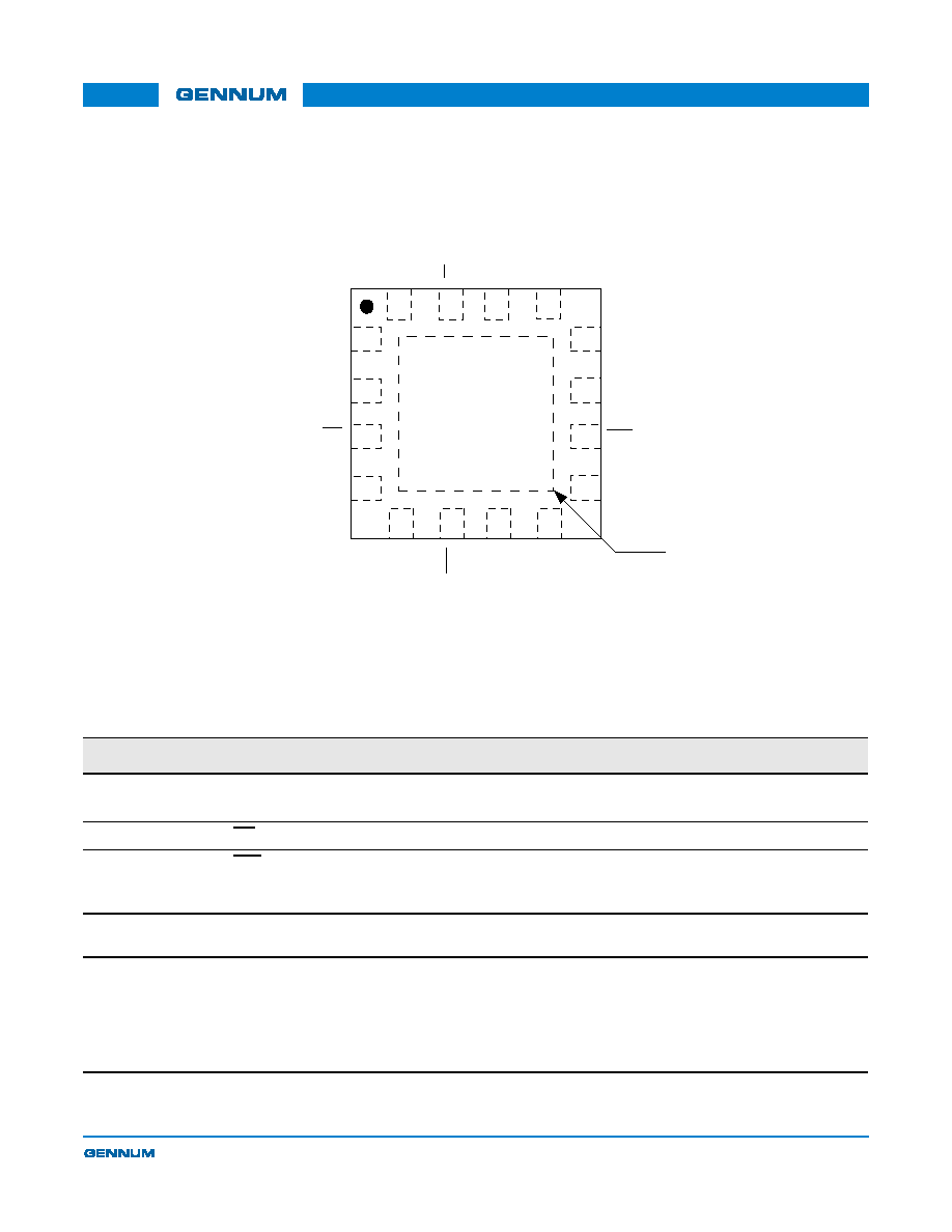
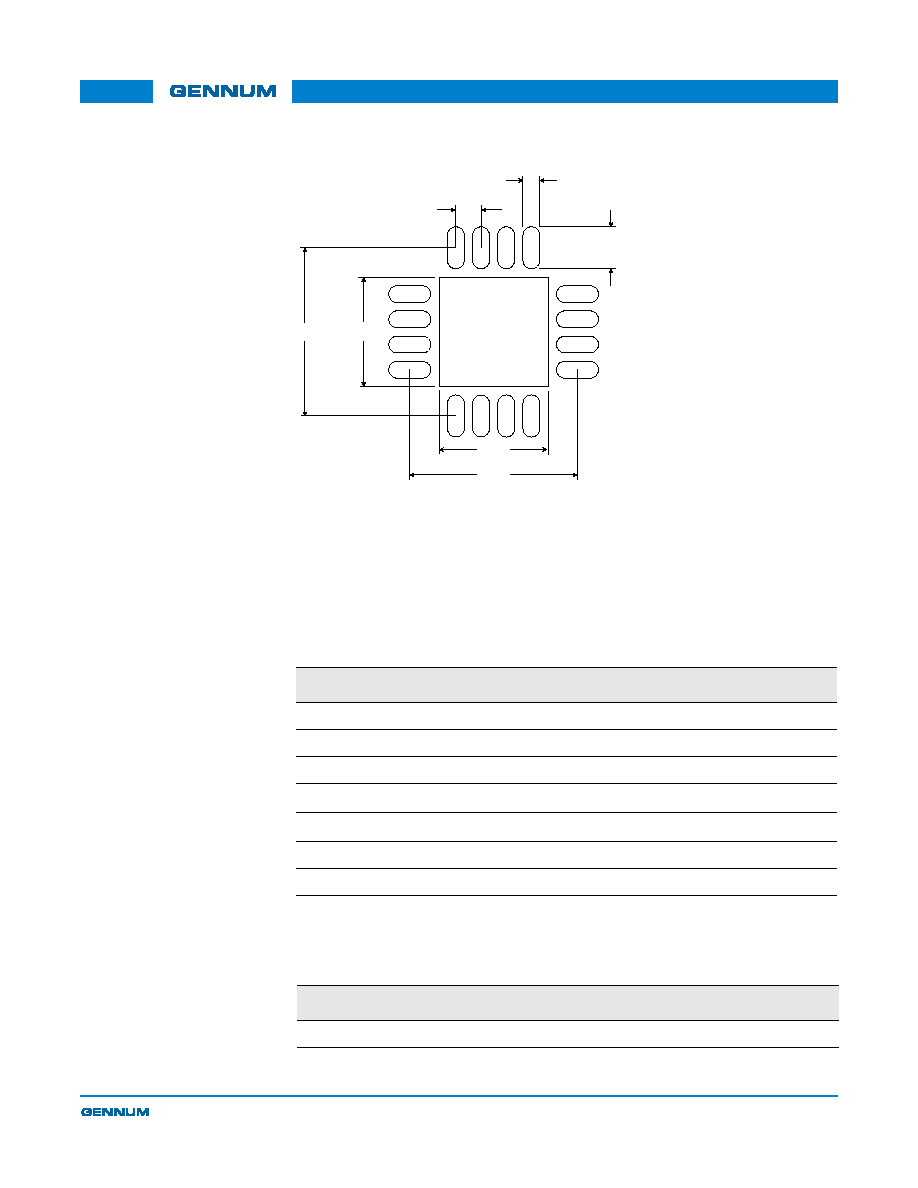
1. Pin Out
1.1 GS1574A Pin Assignment
Figure 1-1: 16-Pin QFN
1.2 GS1574A Pin Descriptions
GS1574A
(top view)
1
V
EE
_A
V
EE
_A
SDI
SDI
2
3
4
SDO
SDO
V
EE
_D
V
EE
_D
12
11
10
9
AGC
AGC
BYPASS
MCLADJ
5
7
6
8
V
CC
_A
MUTE
CD
V
CC
_D
13
14
15
16
Center Pad
(bottom of package, internally
bonded to VEE_A)
Table 1-1: GS1574A Pin Descriptions
Pin Number
Name
Timing
Type
Description
1, 4
VEE_A
Analog
Power
Most negative power supply for analog circuitry.
Connect to GND.
2, 3
SDI, SDI
Analog
Input
Serial digital differential input.
5, 6
AGC, AGC
Analog
≠
External AGC capacitor.
Connect pin 5 and pin 6 together as shown in the
Typical Application
Circuit on page 13
.
7
BYPASS
Not
Synchronous
Input
Forces the Equalizing and DC RESTORE stages into bypass mode
when HIGH. No equalization occurs in this mode.
8
MCLADJ
Analog
Input
Maximum cable length adjust.
Adjusts the approximate maximum amount of cable to be equalized
(from 0m to the maximum cable length). The output is muted (latched to
the last state) when the maximum cable length is achieved.
NOTE: MCLADJ is only recommended for data rates up to 360Mb/s.
For data rates above this, MCLADJ should be left floating.

GS1574A Data Sheet
33416 - 5
March 2006
4 of 16
9
VEE_D
Analog
Power
Most negative power supply for the digital circuitry and output buffer.
Connect to GND.
10, 11
SDO, SDO
Analog
Output
Equalized serial digital differential output.
12
VEE_D
Analog
Power
Most negative power supply for the digital circuitry and output buffer.
Connect to GND.
13
VCC_D
Analog
Power
Most positive power supply for the digital I/O pins of the device.
Connect to +3.3V DC.
14
MUTE
Not
Synchronous
Input
CONTROL SIGNAL INPUT
levels are LVCMOS/LVTTL compatible. (3.3V Tolerant)
When the MUTE pin is set HIGH by the application interface, the serial
digital output of the device will be forced to a steady state.
When the MUTE pin is set LOW, the serial digital output of the device
will be active.
NOTE: This pin may be connected directly to the CD pin to allow mute
on loss of carrier.
15
CD
Not
Synchronous
Output
STATUS SIGNAL OUTPUT
Signal levels are LVCMOS/LVTTL compatible.
Indicates the presence of a good input signal.
When the CD pin is LOW, a good input signal has been detected.
When this pin is HIGH, the input signal is invalid.
This pin will indicate loss of carrier for data rates > 19Mb/s.
16
VCC_A
Analog
Power
Most positive power supply for the analog circuitry of the device.
Connect to +3.3V DC.
≠
Center Pad
≠
Power
Internally bonded to VEE_A.
Table 1-1: GS1574A Pin Descriptions (Continued)
Pin Number
Name
Timing
Type
Description

GS1574A Data Sheet
33416 - 5
March 2006
5 of 16
2. Electrical Characteristics
2.1 Absolute Maximum Ratings
2.2 DC Electrical Characteristics
Parameter
Value
Supply Voltage
-0.5V to +3.6 V
DC
Input ESD Voltage
2kV
Storage Temperature Range
-50∞C < T
s
< 125∞C
Input Voltage Range (any input)
-0.3 to (V
CC
+0.3)V
Operating Temperature Range
0∞C to 70∞C
Solder Reflow Temperature
260∞C
Table 2-1: DC Electrical Characteristics
V
DD
= 3.3V, T
A
= 0∞C to 70∞C, unless otherwise shown
Parameter
Symbol
Conditions
Min
Typ
Max
Units
Notes
Supply Voltage
V
CC
≠
3.135
3.3
3.465
V
±5%
Power Consumption
P
D
T
A
= 25∞C
≠
215
≠
mW
≠
Supply Current
I
s
T
A
= 25∞C
≠
65
≠
mA
≠
Output Common Mode Voltage
V
CMOUT
T
A
= 25∞C
≠
V
CC
-
V
SDO
/2
≠
V
≠
Input Common Mode Voltage
V
CMIN
T
A
= 25∞C
≠
1.75
≠
V
≠
MCLADJ DC Voltage (to mute
signal)
≠
0m, T
A
= 25∞C
≠
1.3
≠
V
≠
MCLADJ Range
≠
T
A
= 25∞C
≠
0.5
≠
V
≠
CD Output Voltage
V
CD(OH)
Carrier not
present
2.4
≠
≠
V
≠
V
CD(OL)
Carrier present
≠
≠
0.4
V
≠
Mute Input Voltage Required to
Force Outputs to Mute
V
Mute
Min to Mute
2.0
≠
≠
V
≠
Mute Input Voltage Required to
Force Outputs Active
V
Mute
Max to Activate
≠
≠
0.8
V
≠
GS1574A Data Sheet
33416 - 5
March 2006
6 of 16
2.3 AC Electrical Characteristics
Table 2-2: AC Electrical Characteristics
V
DD
= 3.3V, T
A
= 0∞C to 70∞C, unless otherwise shown
Parameter
Symbol
Conditions
Min
Typ
Max
Units
Notes
Serial input data rate
DR
SDO
≠
143
≠
1485
Mb/s
≠
Input Voltage Swing
V
SDI
T
A
=25∞C, differential
720
800
950
mV
p-p
1
Output Voltage Swing
V
SDO
100
load, T
A
=25∞C,
differential
≠
750
≠
mV
p-p
≠
Maximum Equalized Cable
Length
≠
270Mb/s, Belden 1694A,
350m
≠
0.2
≠
UI
2
≠
270Mb/s, Belden 8281,
280m
≠
0.2
≠
UI
2
≠
1.485Gb/s, Belden 1694A,
140m
≠
0.25
≠
UI
2
≠
1.485Gb/s, Belden 8281,
100m
≠
0.25
≠
UI
2
Output Rise/Fall time
≠
20% - 80%
≠
80
220
ps
≠
Mismatch in rise/fall time
≠
≠
≠
≠
30
ps
≠
Duty cycle distortion
≠
≠
≠
≠
30
ps
≠
Overshoot
≠
≠
≠
≠
10
%
≠
Input Return Loss
≠
≠
15
≠
≠
dB
3
Input Resistance
≠
single ended
≠
1.64
≠
k
≠
Input Capacitance
≠
single ended
≠
1
≠
pF
≠
Output Resistance
≠
single ended
≠
50
≠
≠
NOTES:
1. 0m cable length.
2. Equalizer Pathological.
3. Tested on CB1574A board from 5MHz to 2GHz.

GS1574A Data Sheet
33416 - 5
March 2006
7 of 16
2.4 Solder Reflow Profiles
The device is manufactured with Matte-Sn terminations and is compatible with both
standard eutectic and Pb-free solder reflow profiles. MSL qualification was
performed using the maximum Pb-free reflow profile shown in
Figure 2-1
. The
recommended standard Pb reflow profile is shown in
Figure 2-2
.
Figure 2-1: Maximum Pb-free Solder Reflow Profile (Preferred)
Figure 2-2: Standard Pb Solder Reflow Profile (Pb-free package)
25∞C
150∞C
200∞C
217∞C
260∞C
250∞C
Time
Temperature
8 min. max
60-180 sec. max
60-150 sec.
20-40 sec.
3∞C/sec max
6∞C/sec max
25∞C
100∞C
150∞C
183∞C
230∞C
220∞C
Time
Temperature
6 min. max
120 sec. max
60-150 sec.
10-20 sec.
3∞C/sec max
6∞C/sec max

GS1574A Data Sheet
33416 - 5
March 2006
8 of 16
Figure 2-3: Test Circuit
GigaBERT
1400
EXT.
CLOCK
CLOCK
OUT
DATA
OUT
EXT.
CLOCK
1.485GHz/270MHz
GS1574A
TEST BOARD
TDS 820
CH. 1
CH. 2
OUT
IN
OUT
EXT. TRIGGER
50/75
8281 or 1694A CABLE
GS1574A Data Sheet
33416 - 5
March 2006
9 of 16
3. Input / Output Circuits
Figure 3-1: Input Equivalent Circuit
Figure 3-2: MCLADJ Equivalent Circuit
Figure 3-3: Output Circuit
3k
3.6k
3k
3.6k
RC
SDI
SDI
V
CC
MCLADJ
12.2k
150µ
+
-
50
50
SDO
SDO
GS1574A Data Sheet
33416 - 5
March 2006
10 of 16
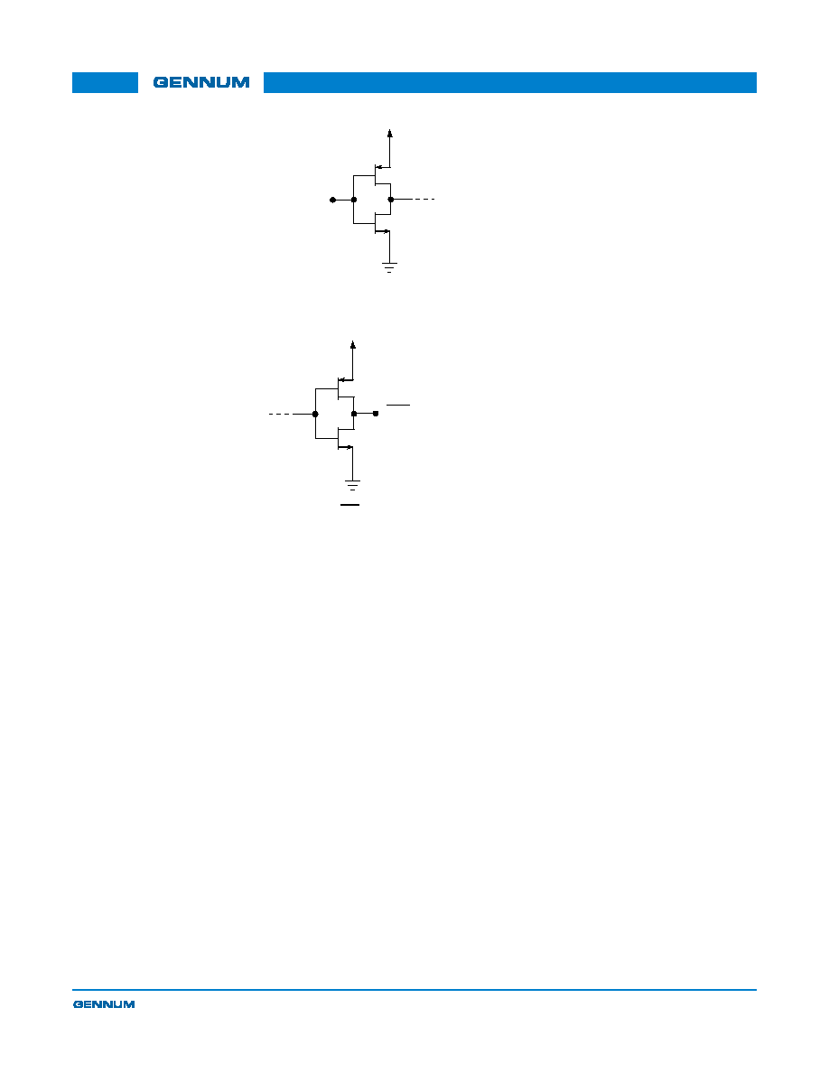
Figure 3-4: MUTE and BYPASS Circuits
Figure 3-5: CD Circuit
MUTE,
BYPASS
CD

GS1574A Data Sheet
33416 - 5
March 2006
11 of 16
4. Detailed Description
The GS1574A is a high speed BiCMOS IC designed to equalize serial digital
signals.
The GS1574A can equalize both HD and SD serial digital signals, and will typically
equalize greater than 140m of Belden 1694A cable at 1.485Gb/s and 350m at
270Mb/s.
The GS1574A is powered from a single +3.3V power supply and consumes
approximately 215mW of power.
4.1 Serial Digital Inputs
The serial data signal may be connected to the input pins (SDI/SDI) in either a
differential or single ended configuration. AC coupling of the inputs is
recommended, as the SDI and SDI inputs are internally biased at approximately
1.8V.
4.2 Cable Equalization
The input signal passes through a variable gain equalizing stage whose frequency
response closely matches the inverse of the cable loss characteristic. In addition,
the variation of the frequency response with control voltage imitates the variation
of the inverse cable loss characteristic with cable length.
The edge energy of the equalized signal is monitored by a detector circuit which
produces an error signal corresponding to the difference between the desired edge
energy and the actual edge energy. This error signal is integrated by both an
internal and an external AGC filter capacitor providing a steady control voltage for
the gain stage. As the frequency response of the gain stage is automatically varied
by the application of negative feedback, the edge energy of the equalized signal is
kept at a constant level which is representative of the original edge energy at the
transmitter. The equalized signal is also DC restored, effectively restoring the logic
threshold of the equalized signal to its correct level independent of shifts due to AC
coupling. The digital output signals have a nominal voltage of 750mV
pp
differential,
or 375mV
pp
single ended when terminated with 50
as shown in
Figure 4-1
.

GS1574A Data Sheet
33416 - 5
March 2006
12 of 16
Figure 4-1: Typical Output Voltage Levels
4.3 Programmable Mute Output
For SMPTE 259M inputs, the GS1574A incorporates a programmable threshold
output mute (MCLADJ).
In applications where there are multiple input channels using the GS1574A, it is
advantageous to have a programmable mute output to avoid signal crosstalk.
The output of the GS1574A can be muted when the input signal decreases below
a certain input level. This threshold is determined using the input voltage applied
to the MCLADJ pin. The MCLADJ pin may be left unconnected for applications
where output muting is not required.
This feature has been designed for use in applications such as routers where
signal crosstalk and circuit noise cause the equalizer to output erroneous data
when no input signal is present. The use of a Carrier Detect function with a fixed
internal reference does not solve this problem since the signal to noise ratio on the
circuit board could be significantly less than the default signal detection level set by
the on chip reference.
NOTE: MCLADJ is only recommended for data rates up to 360Mb/s. For data rates
above this, MCLADJ should be left floating.
4.4 Mute and Carrier Detect
The GS1574A includes a MUTE input pin that allows the application interface to
mute the serial digital output at any time. Set the MUTE pin HIGH to mute SDO and
SDO. In this case, the outputs will mute regardless of the setting of the BYPASS pin.
A Carrier Detect output pin (CD) indicates the presence of a valid signal at the input
of the GS1574A. When CD is LOW, the device has detected a valid input on SDI
and SDI. When CD is HIGH, the device has not detected a valid input.
NOTE: CD will only detect loss of carrier for data rates greater than 19Mb/s. The
CD output pin may be connected directly to the MUTE input pin to enable automatic
muting of the GS1574A when no valid input signal has been detected.
NOTE: If the maximum cable length is exceeded and the device is not in bypass
mode the GS1574A will not assert the CD pin even if a carrier is present.
50
50
SDO
SDO
+187.5mV
-187.5mV
V
CM
= 2.925V
typical
+187.5mV
-187.5mV
V
CM
= 2.925V
typical

GS1574A Data Sheet
33416 - 5
March 2006
13 of 16
5. Application Information
5.1 PCB Layout
Special attention must be paid to component layout when designing serial digital
interfaces for HDTV. An FR-4 dielectric can be used, however, controlled
impedance transmission lines are required for PCB traces longer than
approximately 1cm. Note the following PCB artwork features used to optimize
performance:
∑
PCB trace width for HD rate signals is closely matched to SMT component
width to minimize reflections due to change in trace impedance.
∑
The PCB ground plane is removed under the GS1574A input components to
minimize parasitic capacitance.
∑
The PCB ground plane is removed under the GS1574A output components to
minimize parasitic capacitance.
∑
High speed traces are curved to minimize impedance changes.
5.2 Typical Application Circuit
Figure 5-1: GS1574A Typical Application Circuit
GS1574A
SDI
CD
SDI
VEE_D
MUTE
VCC_D
AGC
BYPASS
MCLADJ
VEE_A
NOTE: All resistors in Ohms, capacitors in Farads,
and inductors in Henrys, unless otherwise noted.
VEE_A
AGC
VCC_A
SDO
SDO
VEE_D
10n
1
10n
SDO
4u7
4u7
+
+
SDO
CD
MUTE
VCC
BYPASS
MCLADJ
470n
6.2n
75
SDI
1u
75
1u
37R4
VCC
4
5
6
2
3
8
7
16
12
13
11
14
15
9
10
470n

GS1574A Data Sheet
33416 - 5
March 2006
14 of 16
6. Package & Ordering Information
6.1 Package Dimensions
4.00+/-0.05
B
4.00+/-0.05
2X
2X
0.15
0.15
C
C
0.10 C
16X
0.08 C
SEATING PLANE
0.85+/-0.05
0.00-0.05
0.65/2
0.65
DETAIL B
SCALE:NTS
DATUM A OR B
TERMINAL TIP
0.20 REF
DATUM B
0.65
16X
0.35+/-0.05
0.10
0.05
C
A B
C
DATUM A
2.76+/-0.10
0.40+/-0.05
2.76+/-0.10
DETAIL B
CENTER TAB
PIN 1 AREA
A
C
GS1574A Data Sheet
33416 - 5
March 2006
15 of 16
6.2 Recommended PCB Footprint
The Center Pad should be connected to the most negative power supply plane for
analog circuitry in the device (VEE_A) by a minimum of 5 vias.
Note: Suggested dimensions only. Final dimensions should conform to customer
design rules and process optimizations.
6.3 Packaging Data
6.4 Ordering Information
0.35
0.55
2.76
3.70
2.76
3.70
NOTE: All dimensions
are in millimeters.
0.65
CENTER PAD
Parameter
Value
Package Type
4mm x 4mm 16-pin QFN
Package Drawing Reference
JEDEC M0220
Moisture Sensitivity Level
3
Junction to Case Thermal Resistance,
j-c
31.0∞C/W
Junction to Air Thermal Resistance,
j-a
(at zero airflow)
43.8∞C/W
Psi
11.0∞C/W
Pb-free and RoHS compliant
Yes
Part Number
Package
Temperature Range
GS1574A
GS1574ACNE3
16-pin QFN
0∞C to 70∞C

CAUTION
ELECTROSTATIC SENSITIVE DEVICES
DO NOT OPEN PACKAGES OR HANDLE
EXCEPT AT A STATIC-FREE WORKSTATION
GENNUM CORPORATION
Mailing Address: P.O. Box 489, Stn. A, Burlington, Ontario, Canada L7R 3Y3
Shipping Address: 970 Fraser Drive, Burlington, Ontario, Canada L7L 5P5
Tel. +1 (905) 632-2996 Fax. +1 (905) 632-5946
GENNUM JAPAN CORPORATION
Shinjuku Green Tower Building 27F, 6-14-1, Nishi Shinjuku, Shinjuku-ku, Tokyo, 160-0023 Japan
Tel. +81 (03) 3349-5501, Fax. +81 (03) 3349-5505
GENNUM UK LIMITED
25 Long Garden Walk, Farnham, Surrey, England GU9 7HX
Tel. +44 (0)1252 747 000 Fax +44 (0)1252 726 523
Gennum Corporation assumes no liability for any errors or omissions in this document, or for the use of the
circuits or devices described herein. The sale of the circuit or device described herein does not imply any
patent license, and Gennum makes no representation that the circuit or device is free from patent infringement.
GENNUM and the G logo are registered trademarks of Gennum Corporation.
© Copyright 2004 Gennum Corporation. All rights reserved. Printed in Canada.
www.gennum.com
GS1574A Data Sheet
33416 - 5
March 2006
16
16 of 16
DOCUMENT IDENTIFICATION
DATA SHEET
The product is in production. Gennum reserves the right to make
changes to the product at any time without notice to improve reliability,
function or design, in order to provide the best product possible.
7. Revision History
Version
ECR
PCN
Date
Changes and/or Modifications
0
136149
≠
March 2005
Converted to Preliminary Data Sheet.
Updated typical application circuit.
Updated Input/Output circuits. Updated
AC and DC electrical characteristics.
Updated description of MUTE and CD
functionality. Correced minor typing
errors. Updated center pad dimensions
on PCB footprint.
1
136885
≠
May 2005
Corrected description of connection for
AGC and AGC pins in the Pin
Description table. Clarified solder reflow
profile descriptions. Corrected minor
typing errors.
2
137167
≠
June 2005
Rephrased RoHS compliance
statement.
3
137321
≠
June 2005
Amended notes on use of MCLADJ
above 360 Mb/s.
4
137744
≠
September 2005
Convert to Data Sheet. Corrected typing
errors. Corrected process to BiCMOS.
5
139634
38695
March 2006
Corrected pad standoff height and
tolerances for pad width & package
dimension. Corrected pad shape.