 | –≠–ª–µ–∫—Ç—Ä–æ–Ω–Ω—ã–π –∫–æ–º–ø–æ–Ω–µ–Ω—Ç: GS4882 | –°–∫–∞—á–∞—Ç—å:  PDF PDF  ZIP ZIP |

Document No. 521 - 61 - 01
DATA SHEET
GENNUM CORPORATION P.O. Box 489, Stn A, Burlington, Ontario, Canada L7R 3Y3 tel. (905) 632-2996 fax: (905) 632-5946
Gennum Japan: Shinjuku Green Tower Building 27F 6-14-1, Nishi Shinjuku Shinjuku-ku, Tokyo 160-0023 Japan Tel: +81 (03) 3349-5501 Fax: +81 (03) 3349-5505
Patent Pending.
GS4882, GS4982 Video Sync
Separators with 50% Sync Slicing
FEATURES
DESCRIPTION
The GS4882 and GS4982 are precision sync separators for
extracting timing information from NTSC, PAL, and SECAM
video signals. The GS4882 generates noise immune and
temperature stable composite sync, vertical sync, back porch
and odd/even field signals. The GS4982 provides a horizontal
sync output for those applications requiring horizontal sync
extraction.
The GS4882 and GS4982 feature an internal color burst filter
for minimization of spurious timing information and the reduction
of external component count. The precision 50% sync slicing
feature embodied in the device provides for superior sync
extraction in the presence of noise and varying sync pulse
amplitudes. The high performance dual mode input clamp
aids in maintaining the accuracy of the internally derived 50%
sync slicing level to within ±5% as well in reducing system
start-up/recovery time. In addition, a missing pulse detector
enables the devices to quickly respond to impulse noise by
temporarily turning on a Nosync Recovery Current connected
to the dual mode input clamp. The input stage will operate with
input signal amplitudes ranging from +0.5 to +4.0V peak to
peak with a +5V supply voltage.
The GS4882 and GS4982 have robust signal detection and
output muting circuitry. Should valid video be removed from
the device input, the absence of video will be automatically
detected and all outputs muted to a logic high state after a
defined probation period. Upon the return of a valid video
signal, device outputs are enabled after receiving 8 lines of
video. An internal frequency to voltage converter also allows
the device to differentiate between valid and invalid input
signals by analyzing the horizontal scan rate of the input signal
and comparing it against the expected input signal scan rate.
The GS4882 and GS4982 are available in standard 8 pin PDIP
and SOIC packages, operate with a + 4.5 to +13.2 volt supply
voltage range and typically consume less than 6 mA of current
with a +5 V supply voltage.
∑ precision 50% sync slicing
∑ internal color burst filter
∑ ±5 ns temperature stability
∑ superior noise immunity
∑ robust signal detection/output muting circuitry
∑ high performance dual mode input clamp
∑ 0.5 V to 4.0 Vpp input signal with +5 V supply
∑ composite, vertical, back porch, odd/even outputs
∑ horizontal sync output available with GS4982
∑ +4.5 V to +13.2 V supply voltage range
∑ Pb-free and Green
R
SET
GROUND
V
cc
VERTICAL
SYNC OUT
1
2
3
4
8
7
6
5
GROUND
V
cc
1
2
3
4
8
7
6
5
GS4882
VERTICAL
SYNC OUT
R
SET
GS4982
ODD/EVEN
BACK PORCH
BACK PORCH
ODD/EVEN
PIN CONNECTIONS
COMPOSITE
SYNC OUT
COMPOSITE
VIDEO IN
HORIZONTAL
COMPOSITE
VIDEO IN
Revision date: July 2004
Part Number
Package
Temperature
Pb-Free
Type
Range
and Green
GS4882-CDA
8 pin PDIP
0∞ C to 70∞ C
No
GS4882-CKA
8 pin SOIC
0∞ C to 70∞ C
No
GS4882-CTA
8 pin SOIC Tape
0∞ C to 70∞ C
No
GS4982-CDA
8 pin PDIP
0∞ C to 70∞ C
No
GS4982-CKA
8 pin SOIC
0∞ C to 70∞ C
No
GS4982-CTA
8 pin SOIC Tape
0∞ C to 70∞ C
No
GS4882-CKAE3
8 pin SOIC
0∞ C to 70∞ C
Yes
GS4982-CKAE3
8 pin SOIC
0∞ C to 70∞ C
Yes
ORDERING INFORMATION
2 of 7
521 - 61 - 01
Supply Voltage
4.5
5.0
13.2
V
Supply Current
Outputs at Logic 1
-
6
10
mA
Signal Level
V
CC
= 5 V
0.5
-
4.0
V
Nosync Recovery Current
23
30
40
µA
Delay to Nosync Recovery
70
-
120
µs
Sync Tip Clamp Voltage
-
1.55
-
V
Source Impedance
-
-
200
Color Burst Filter
Attenuation at 3.58 MHz
12
15
-
dB
Sync Slice Level
Input Amplitude 0.5 to 2.0 Vp-p
45
50
55
%
Delay from Video
T
A
= 25∞ C
150
200
250
ns
Delay from Video
T
A
= 0∞ C to 70∞ C
-5
-
+5
ns
Temperature Stability
Delay
From rising edge of sync
400
525
650
ns
Pulse Width
2.0
2.5
3.2
µs
Pulse Width
Serrations during vertical interval
197. 7
197. 7
197. 7
µs
Delay from Video
340
420
510
ns
Pulse Width
6.0
8.0
10.0
µs
Probation
Period
1.2
2.5
5
ms
Lock Time
-
8
-
lines
R
SET
Ref. Voltage
1.14
1.24
1.34
V
V
OH
I
OH
= 40 µA
4.2
4.6
-
V
I
OH
= 1.6 mA
2.4
3.4
-
V
V
OL
I
OL
= -1.6 mA
-
0.3
0.6
V
ABSOLUTE MAXIMUM RATINGS
PARAMETER
VALUE/UNITS
Supply Voltage
+13.5 V
Operating Temperature Range
0∞C
T
A
70∞C
Storage Temperature Range
-65∞C
T
S
150∞C
Lead Temperature (soldering, 10 seconds)
260∞C
CAUTION
ELECTROSTATIC
SENSITIVE DEVICES
DO NOT OPEN PACKAGES OR HANDLE
EXCEPT AT A STATIC-FREE WORKSTATION
PARAMETER
CONDITIONS MIN TYP MAX UNITS
POWER
SUPPLIES
VIDEO
INPUT
ELECTRICAL CHARACTERISTICS
V
CC
= 5 V, R
SET
= 227 k
, T
A
= 25∞ C, C
L
=15 pF unless otherwise specified.
COMPOSITE
SYNC
OUTPUT
(GS4882)
BACK
PORCH
OUTPUT
VERTICAL
SYNC
OUTPUT
HORIZONTAL
OUTPUT
(GS4982)
OUTPUT
MUTE
LOGIC
OUTPUTS
R
SET
REFERENCE

3 of 7
521 - 61 - 01
CIRCUIT DESCRIPTION
The Block Diagrams for the GS4882 and GS4982 are shown
in Figure 6 and Figure 7, with timing diagrams for the devices
shown in Figure 8.
When presented with a composite video input signal, the
GS4882 outputs composite sync, vertical sync, back porch
and odd/even field information. The GS4982 substitutes the
composite sync output with a horizontal sync output, for those
applications requiring horizontal sync extraction.
An external resistor, R
SET
, connected to pin 6 is used to set all
timing currents in the device. For standard NTSC applications,
R
SET
should be set to 227 k
. The value of R
SET
for a standard
NTSC application is different for the GS4882/GS4982 line of
sync separators(R
SET
= 227 k
) than it is for the GS1881/
GS4881/GS4981 line of sync separators (R
SET
= 680 k
). This
change was made to improve jitter performance of the device.
COMPOSITE VIDEO INPUT (pin 2)
The GS4882 and GS4982 will operate with input signal
amplitudes ranging from 0.5 V to 4.0 V p-p. Composite video
is AC coupled into the device via an external coupling
capacitor connected to pin 2.
Immediately upon entering the GS4882/GS4982 the video
signal is passed to the device's dual mode input clamp in
order to clamp the sync tip of the input video waveform to 1.55
Volts. The GS4882/GS4982's dual mode input clamp, with
both Hard Clamp and Soft Clamp capabilities, has been
specifically designed for use in high performance sync sepa-
ration. The dual mode input clamp aids in maintaining the
accuracy of the internally derived 50% sync slicing level to
within ±5% by utilizing the Soft Clamp during steady state
operation. The device improves system start-up and impulse
noise recovery time by utilizing the device's Hard Clamp and
Nosync Recovery Current during initial start-up and when
steady state operation has been disturbed by impulse noise.
During the clamping operation, the input video signal is
passed through the device's internal color burst filter. The
internal filter attenuates the color burst by typically >15 dB.
Figure 1 shows the typical frequency response of the internal
color burst filter.
The 50% point of sync is determined by using two identical
resistors to divide the voltage between sync tip and back
porch. The importance of precision sync tip clamping may be
appreciated here, since the sync tip voltage is used in deriving
the 50% slicing level. The back porch voltage is derived
through an internal integrate and hold circuit that is gated by
the Back Porch output signal. By integrating over the entire
back porch period, the accuracy and noise immunity of
acquired back porch voltage is greatly improved when
compared to systems using simple sample and hold
techniques.
The output of the comparator is a reproduction of the input
video signal with the active portion of video removed. This
represents the composite sync waveform presented on pin 1
of the GS4882.
The video path and composite sync slicing circuitry have been
optimized and compensated to achieve superior temperature
stability. Variations in composite sync output timing over the
commercial temperature range are less than ±5 ns.
COMPOSITE SYNC OUTPUT (pin 1 GS4882)
The filtered video signal is then fed to a comparator which
compares it to an internally derived voltage corresponding to
the 50% point of the sync pulse amplitude.
By slicing the composite video waveform at 50% of the sync
pulse amplitude, variations in output pulse timing due to
variations in input signal amplitude are minimized. Figure 1
demonstrates the stability of output pulse timing achieved with
50% sync slicing .
0
-5
-15
-25
-35
0.01 0.1 1 10
FREQUENCY (MHz)
GAIN (dB)
Fig. 1 Frequency Response of Internal Color Burst Filter
SYNC PULSE AMPLITUDE
A
A/2
50% Slice
50% Slice
t
o
Time
Sync Pulse No.1
Sync Pulse No.2
With 50% Sync Slicing no Time Base Errors (TBEs)
are introduced due to variations in sync pulse amplitude.
Output pulses are always produced at t
O
+t
D
,
where
t
D
represents the delay through the device.
Fig. 2 Stability of Output Pulse Timing with Variations
in Sync Pulse Amplitude
4 of 7
521 - 61 - 01
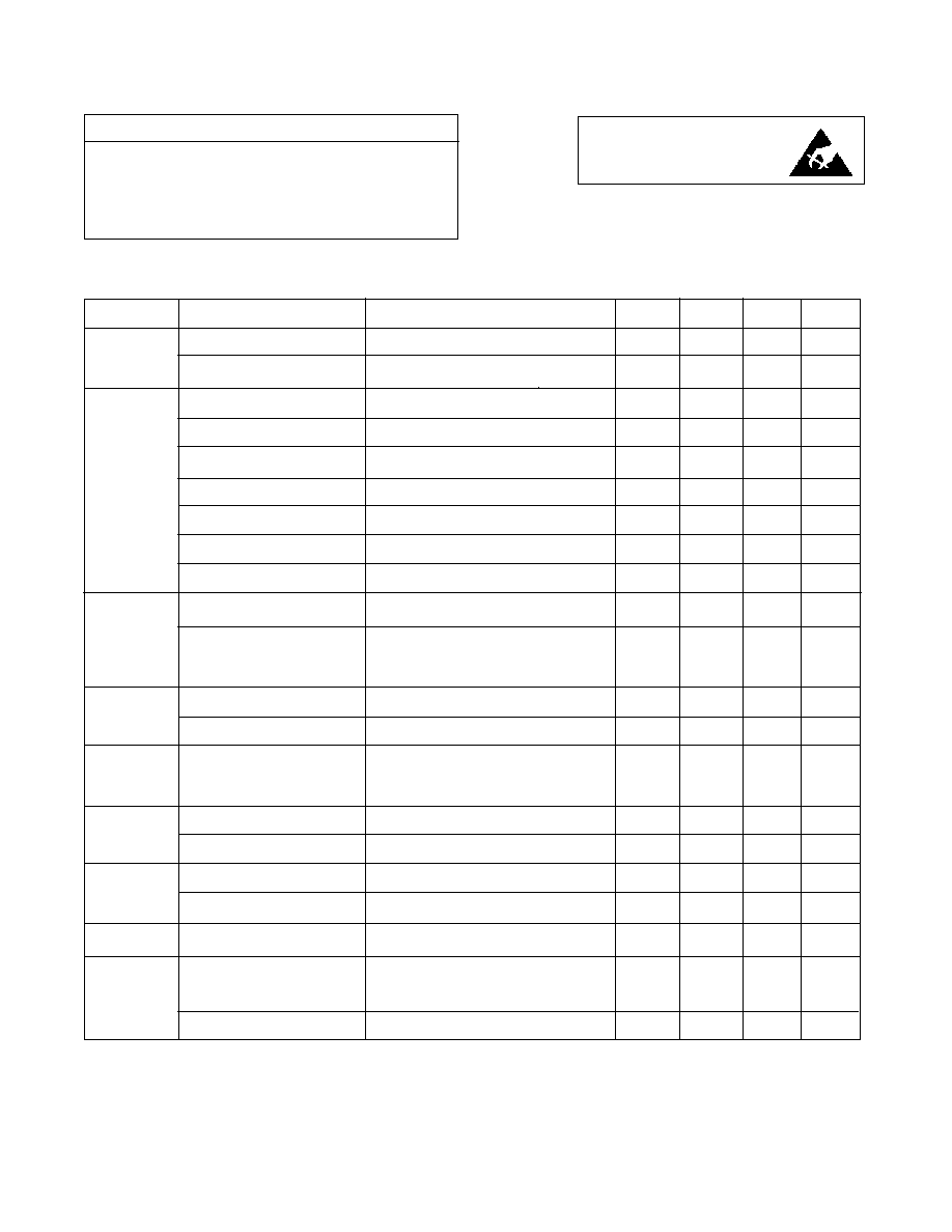
The GS4882 and GS4982 determine odd/even field information
by comparing vertical sync with an internally generated
horizontal sync. This output is clocked out by the falling edge
of vertical sync. The odd/even output is low during even fields
and high during odd fields.
This method of determining odd / even field information
provides for superior noise immunity. Noise during the pre-
equalizing pulses does not affect the output since the field
decision is made at the beginning of the vertical interval. This
noise immunity is displayed in Figure 4 in which an extra pre-
equalizing pulse has been added to the video input with no
negative effect on the odd/even field information.
HORIZONTAL OUTPUT (pin 1 on GS4982)
As mentioned previously, the odd/even field output of the
device is generated by comparing vertical sync with an
internal horizontal sync signal. This horizontal sync signal is
a true horizontal signal (i.e. maintained during the vertical
interval) and is output on pin 1 of the GS4982. A delay of 420
ns and a width of 8.0 µs are typical for this signal. The internal
Windowing Circuit which generates horizontal sync provides
excellent impulse noise immunity as shown in Figure 5.
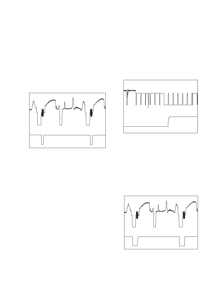
BACK PORCH OUTPUT (pin 5)
In an NTSC composite video signal, horizontal sync pulses
are followed by the back porch interval. The GS4882 and
GS4982 generate a negative going pulse on pin 5 during this
time. It is delayed typically 525 ns from the rising edge of sync
and has a typical width of 2.5 µs.
During the pre-equalizing, vertical sync and post equalizing
periods, composite sync doubles in frequency. The GS4882
and GS4982 maintain the back porch output at the horizontal
rate due to a Back Porch Enable (BPEN) signal, generated by
the internal Windowing Circuit, which forces back porch to be
output at the horizontal rate.
This gating circuit is also the reason for the excellent impulse
noise immunity of the back porch output as shown in Figure 3.
VERTICAL SYNC OUTPUT (pin 3)
The vertical sync interval is detected by integrating the
composite sync pulses. The first broad pulse causes an
internal capacitor to charge past a fixed threshold and raises
an internal vertical flag. Once the vertical flag is raised, the
positive edge of the next serration clocks out the vertical
output. When the vertical sync interval ends, the first post
equalizing pulse is unable to charge the capacitor sufficiently,
causing the vertical interval flag to go high. The rising edge of
the second post-equalizing pulse then clocks out the high flag
to end the vertical sync pulse. The vertical output is clocked
in and out and therefore is a fixed width. Since the vertical
detector is designed as a true integrator, it provides improved
noise immunity.
ODD/EVEN OUTPUT (pin 7)
NTSC, PAL and SECAM composite video standards are
interlaced video schemes and therefore have odd and even
fields. For odd fields, the first broad vertical sync pulse is
coincident with the start of horizontal, while for even fields, the
first broad vertical sync pulse starts in the middle of a
horizontal line.
Impulse
Noise
Video
Input
Odd / Even
Output
Fig. 4 Noise Immunity of Odd/Even Output
Video
Input
Impulse
Noise
Horizontal
Output
Fig. 5 Noise Immunity of Horizontal Sync Output
Even Odd
Video
Input
Back
Porch
Output
Impulse
Noise
Fig. 3 Noise Immunity of Back Porch Output

5 of 7
521 - 61 - 01
ODD / EVEN
OUTPUT
(Pin 7)
V
CC
(Pin 8)
R
SET
(Pin 6)
VERTICAL SYNC
OUTPUT
(PIN 3)
BACK PORCH
DETECTOR
COMPOSITE
SYNC OUTPUT
(Pin 1)
HORIZONTAL
CLEN
VERTICAL
DETECTOR
INTEGRATED
HOLD
FILTER
BESSEL
2
ND
ORDER
SIGNAL
DETECT
MUTE
WINDOWING
CIRCUIT
FAULT
HANDLING
CLAMP
WINDOW
+
+
-
-
BACK PORCH
OUTPUT
(Pin 5)
VOLTAGE
REGULATOR
TIMING
CURRENTS
-
+
CLK Q
D
Q
G
Q
Q
D
CLK
D
Q
Q
227k
0.1
µ
V
HC
V
SC
V
SC
+
-
R
50%
POINT
R
INTEGRATED
HOLD
2
ND
ORDER
BESSEL
FILTER
FAULT
HANDLING
CLAMP
WINDOW
VIDEO
INPUT
(Pin 2)
NO SYNC
BPEN
0.1
µ
Assuming that the sync separator is in steady state operation
with a valid input signal, all outputs will be enabled. Removal
of the input signal, or a significant change in the input signal
frequency, will cause an internal probation timer to be triggered.
While on probation, the sync separator outputs remain
enabled and separated sync is still produced. If a valid input
signal is not returned to the system before the probation time
expires (typically 2.5 ms), all outputs will be muted to logic
high state. Should a valid signal return during the probation
period, and eight lines be received before the probation time
expires, device outputs will remain enabled. Once device
outputs are muted, the device must receive 8 valid lines of
video at the correct horizontal frequency before the outputs
are re-enabled.
SIGNAL DETECT AND OUTPUT MUTE
Internal to the GS4882 and GS4982 is a robust video signal
detection circuit. This circuit provides a reliable control signal
that will enable the sync separator outputs only when a valid
video signal is present. When the input signal is not valid, the
outputs are muted and stay in a logic high state.
The GS4882 and GS4982 differentiate between valid and in-
valid input signals by feeding the horizontal sync information
into a frequency to voltage converter. The horizontal scan rate
of the input signal is then compared to an expected input
signal horizontal scan rate. With R
SET
=227 k
, the sync
separator will typically define a valid input signal as one with
a horizontal frequency of 15.7 ± 4 kHz.
Fig. 6 GS4882 Block Diagram
ODD / EVEN
OUTPUT
(Pin 7)
V
CC
(Pin 8)
R
SET
(Pin 6)
VERTICAL SYNC
OUTPUT
(PIN 3)
BACK PORCH
DETECTOR
HORIZONTAL
(Pin 1)
HORIZONTAL
VERTICAL
DETECTOR
SIGNAL
DETECT
MUTE
+
+
-
-
BACK PORCH
OUTPUT
(Pin 5)
VOLTAGE
REGULATOR
TIMING
CURRENTS
-
-
+
+
CLK Q
D
Q
G
Q
Q
D
CLK
D
Q
Q
227k
0.1
µ
R
50%
POINT
R
2
ND
ORDER
BESSEL
FILTER
VIDEO
INPUT
(Pin 2)
NO SYNC
0.1
µ
WINDOWING
CIRCUIT
CLAMP
WINDOW
INTEGRATED
HOLD
FAULT
HANDLING
V
SC
V
HC
V
SC
CLEN
BPEN
Fig. 7 GS4982 Block Diagram