 | –≠–ª–µ–∫—Ç—Ä–æ–Ω–Ω—ã–π –∫–æ–º–ø–æ–Ω–µ–Ω—Ç: GS7000 | –°–∫–∞—á–∞—Ç—å:  PDF PDF  ZIP ZIP |
GENNUM CORPORATION P.O. Box 489, Stn. A, Burlington, Ontario, Canada L7R 3Y3
Tel. +1 (905) 632-2996 Fax. +1 (905) 632-5946 E-mail: info@gennum.com
www.gennum.com
Revision Date: August 1999
Document No. 522 - 06 - 02
PRELIMINARY DATA SHEET
G
S
7
000
FEATURES
∑ fully integrated 270Mb/s SDI receiver or transmitter
∑ fully compliant with SMPTE 259M-C
∑ lock and carrier detect output indication
∑ performance from 0 - 85∞C
RECEIVER FUNCTION
∑ accepts SMPTE 259M-C 270Mb/s serial digital video
and outputs SMPTE 125M compliant 27Mb/s parallel
digital video and clock
∑ integrated cable equalization (beyond 100m Belden
8281)
∑ ease of design use and adjustment free operation
∑ H timing signal output
TRANSMITTER FUNCTION
∑ accepts SMPTE 125M (27Mb/s) parallel video data and
clock, outputs SMPTE 259M-C 270Mb/s serial digital
video
∑ integrated cable driver provides one differential output
(or two single-ended outputs)
APPLICATIONS
Space limited, low power 270Mb/s serial to parallel or
parallel to serial interfaces; Alternate, broadcast quality
uncompressed video interface for industrial and
professional video equipment using the IEEE P1394
interface.
DESCRIPTION
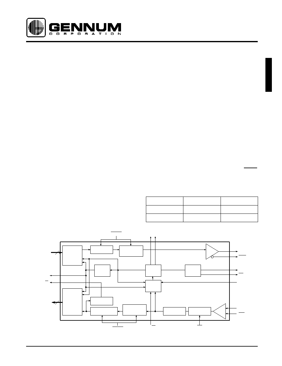
The GS7000 is a dual function IC capable of operating as
either a 270Mb/s Serial Digital Video receiver or a 270Mb/s
Serial Digital Video transmitter. The GS7000 is designed so
that it can be programmed to operate in either receive or
transmit mode via a mode select pin.
When operating as a receiver, the serial data input accepts
SMPTE 259M-C compliant signals. Line terminations are on
the device. An on-chip by-passable fixed gain equalizer
provides cable equalization beyond 100m of high quality
co-axial cable. The clock recovery is performed on chip
with minimal external components. Incoming Serial Digital
Video data is decoded using a NRZI decoder and SMPTE
descrambler to provide clocked SMPTE 125M compliant
parallel output. The SMPTE descrambler and NRZI
decoding functions can be disabled.
When operating as a transmitter, the GS7000 accepts
parallel SMPTE 125M compliant ten bit video. An on-chip
scrambler and NRZI encoder converts the parallel data into
a bit serial SMPTE 259M-C compliant NRZI output signal
suitable for driving co-axial cable. Through the SMPTE
select pin, the SMPTE scrambler and NRZI coding functions
can be disabled.
BLOCK DIAGRAM
ORDERING INFORMATION
PART NUMBER
PACKAGE
TEMPERATURE
GS7000-CQT
52 pin MQFP
0∞C to 85∞C
GS7000-CTT
52 pin MQFP Tape
0∞C to 85∞C
P to S
S to P
SCRAMBLER
NRZI
ENCODER
DESCRAMBLER
TRS
DETECTOR
NRZI
DECODER
f/10
PLL
MUX
SLICER
EQUALIZER
SIGNAL
LOCK
DETECT
SDO
SDO
SDI
SDI
LOCK
CD
PCLK
IN
EQ
Rx/Tx
D
IN (0,9)
D
OUT(0,9)
PCLK
OUT
H
C
1
C
2
10
10
SMPTE
SMPTE
PRO-LINX
TM
GS7000
Serial Digital Video Transceiver
522 - 06 - 02
2
G
S
700
0
ABSOLUTE MAXIMUM RATINGS
PARAMETER
VALUE
Supply Voltage
5.5V
Input Voltage Range (any input)
V
EE
< V
IN
< V
CC
DC Input Current (any one input)
10mA
Power Dissipation (V
CC
= 5.25 V)
830mW
Maximum Die Temperature
125∞C
Operating Temperature Range
0∞C
T
A
85∞C
Storage Temperature Range
-65∞C
T
S
150∞C
Lead Temperature (soldering 10s)
260∞C
AC ELECTRICAL CHARACTERISTICS (Receiver Mode)
V
CC
= 5V, V
EE
= 0V, T
A
= 0∞C to 85∞C, unless otherwise specified.
Serial Data Rate = 270Mb/s, Parallel Data Rate = 27Mb/s, f
PCLK
= 27MHz
PARAMETER
CONDITIONS
SYMBOL
MIN
TYP
MAX
UNITS
NOTES
TEST
LEVEL
Parallel Data Output - Rise/Fall Time
C
L
= 20pF
t
R/F_PDO
1.0
-
6.0
ns
1
1
PCLK rising edge to D
OUT(n)
center
t
D
-
-
± 5
ns
2, 3
1
PCLK rise/fall time
C
L
= 20pF
t
R/F_PCLKo
0.5
-
3.0
ns
1
1
Input Return Loss
75
match
5MHz -> 270MHz
LOSS
IN
-
17
-
dB
6
Asynchronous Lock Time
t
LOCK_ASYNC
-
-
250
ms
4
1
Synchronous Lock Time
t
LOCK_SYNC
-
-
10
µs
5
1
Input Jitter Tolerance
pathological Input
t
J_SI
-
0.4
-
U.I.
6
4
Output PCLK Jitter
pathological Input
t
J_PCLKo
-
1000
-
ps p-p
6
1
Max Error Free Cable Length
pathological Input
75
100
-
m
6, 7
1, 4
NOTES
1. Rise/Fall time is defined as the time for the signal to rise from 20% to 80% of the specified p-p value,
or to fall from 80% to 20% of the specified value.
2. Refer also to Figure 21.
3. This is the time difference between the rising edge of PCLK
OUT
and the center of the bit period.
4. This is the time delay between a valid serial TRS signal on the input, to the moment valid data
appears on the parallel outputs.
5. This is the time for the PLL to re-lock when video streams are switched during the vertical blanking
interval in accordance with SMPTE RP168-1993. The two streams may be 180∞ out of phase with
respect to one another, but pixel aligned.
6. This pathological pattern is defined in SMPTE RP178-1996, paragraphs 4.1 and 4.3.
7. "Error free" is defined as no single bit errors over a period of 10 minutes, using Belden 8281 Cable
and 75
connections. The MIN value is fully tested and the TYP value is based on using the
EB7000 Evaluation Board.
TEST LEVELS
1. 100% tested at 25 ∞C
2. Guaranteed by design
3. Inferred or correlated
value
4. Evaluated using test
setup Figure 1a.
5. Evaluated using test
setup Figure 1b.
6. Evaluated using test
setup Figure 1c.
522 - 06 - 02
3
G
S
7
000
AC ELECTRICAL CHARACTERISTICS (Transmitter Mode)
V
CC
= 5V, V
EE
= 0V, T
A
= 0∞C to 85∞C, unless otherwise specified in `conditions'
Serial Data Rate = 270Mb/s, Parallel Data Rate = 27Mb/s, f
PCLK
= 27MHz
PARAMETER
CONDITIONS
SYMBOL
MIN
TYP
MAX
UNITS
NOTES
TEST
LEVEL
Parallel Data Inputs - rise/fall time
t
R/F_DPI
0.5
10
ns
1
2
Parallel Data Inputs - setup
t
SETUP
4
-
-
ns
8
1
Parallel Data Inputs - hold
t
HOLD
4
-
-
ns
8
1
Parallel Data Inputs - high
V
CC
= 5.25V
V
DPI
2.0
-
V
CC
V
1
Parallel Data Inputs - low
V
CC
= 4.75V
V
DPI
V
EE
-
0.8
V
1
Parallel Clock Input - rise/fall time
t
R/F_PCLK
0.5
-
4
ns
2
Serial Data Output - signal swing
V
CC
= 4.75 - 5.25V
V
DSO
720
800
880
mV p-p
9, 10
1
Serial Data Output - high
V
OH
-
V
CC
- 0.8
-
V
11
2
Serial Data Output - low
V
OL
-
V
CC
- 1.6
-
V
11
2
Serial Data Output - rise/fall time
t
R/F
400
600
1500
ps
1
1
Serial Data Output - jitter
V
CC
= 4.75V
t
J_DSO
-
-
675
ps p-p
12
1
Lock Time
t
LOCK
-
-
250
ms
13
1
Output Return Loss
270MHz
15
-
-
dB
6
NOTES
8. Refer to Figure 26.
9. The outputs are capable of driving a 75
single-ended load, terminated to ground.
10.This value is measured after the resistor network at the SDI outputs shown in Figure 2.
11.Typical PECL values
12.6
additive intrinsic jitter contribution based on pathological input signal
13.This is the lapsed time between valid parallel TRS input to valid serial output
TEST LEVELS
1. 100% tested at 25∞C
2. Guaranteed by design
3. Inferred or correlated value
4. Evaluated using test setup Figure 1a.
5. Evaluated using test setup Figure 1b.
6. Evaluated using test setup Figure 1c.
DC ELECTRICAL CHARACTERISTICS
V
CC
= 5V, V
EE
= 0V, T
A
= 0∞C to 85∞C, unless otherwise specified.
Serial Data Rate = 270Mb/s, Parallel Data Rate = 27Mb/s, f
PCLK
= 27MHz
PARAMETER
CONDITIONS
SYMBOL
MIN
TYP
MAX
UNITS
TEST LEVEL
Positive Supply Voltage
V
CC
+ 4.75
+ 5.00
+ 5.25
V
Supply Current - Receive Mode
V
CC
= 5.25V
I
CC
-
150
-
mA
1
Supply Current - Transmit Mode
V
CC
= 5.25V
I
CC
-
130
-
mA
1
Power Consumption - Receive Mode
V
CC
= 5.25V
P
D
-
750
-
mW
3
Power Consumption - Transmit Mode
V
CC
= 5.25V
P
D
-
650
-
mW
3
Logic Inputs - Low
V
CC
= 5.25V
V
IL
V
EE
-
0.8
V
2
Logic Inputs - High
V
CC
= 4.75V
V
IH
2.0
-
V
CC
V
2
Logic Outputs - Low
V
CC
= 5.25V
V
OL
V
EE
-
0.5
V
2
Logic Outputs - High
V
CC
= 4.75V
V
OH
2.4
-
V
CC
V
2
522 - 06 - 02
4
G
S
700
0
Fig. 1a Test Setup for Jitter Measurements
Fig. 1b Test Setup for Error-Free Cable Length
Fig. 1c Test Setup for Return Loss Measurements
Fig. 2 Test Circuit (Half Duplex Operation)
EB7000
BOARD
GS9028
CABLE
DRIVER
TEKTRONIX
TDS 820
SCOPE
TEKTRONIX
GigaBERT
1400
TRANSMITTER
BELDEN 8281
CABLE
DATA
DATA
CLOCK
TRIGGER
EB7000
BOARD
EB9021
EDH ERROR
COUNTER
TEKTRONIX
VIDEO SlGNAL
GENERATOR
BELDEN 8281
CABLE
VIDEO STREAM
WITH EDH
EB7000
BOARD
HP 4195A
NETWORK
ANALYSER
BELDEN 8281
CABLE
HP 4195A
NETWORK
ANALYSER
BELDEN 8281
CABLE
GS7000
NC
D
IN0
D
IN1
D
IN2
D
IN3
D
IN4
D
IN5
D
IN6
D
IN7
D
IN8
D
IN9
H
NC
NC
D
OUT0
D
OUT1
D
OUT2
D
OUT3
D
OUT4
D
OUT5
D
OUT6
D
OUT7
D
OUT8
D
OUT9
LOCK
NC
NC
V
EE3
SDO
SDO
V
CC3
CD
SMPTE
NC
NC
PCLK
OUT
V
DD
V
SS
NC
NC
V
EE1
C
1
C
2
V
CC1
SDI
SDI
V
CC2
PCLK
IN
V
EE2
EQ
Rx/Tx
NC
OUT
10u
10u
10k
V
CC
825
7.5
7.5
V
CC
100n
220
V
CC
33
100n
V
CC
PARALLEL CLOCK OUT
V
CC
220
10k
Rx/Tx
V
CC
V
CC
EQ
MODE
V
CC
10u
10u
100n
100n
100n
SERIAL DIGITAL IN
10p
10p
33
PARALLEL CLOCK IN
V
CC
10u
100n
PARALLEL
DATA
INPUTS
PARALLEL
DATA
OUTPUTS
LOCK
CD
SERIAL DIGITAL
1
2
3
4
5
6
7
8
9
10
11
12
13
39
38
37
36
35
34
33
32
31
30
29
28
27
All resistors in ohms,
all capacitors in farads,
unless otherwise shown.
52 51 50 49 48 47 46 45 44 43 42 41 40
14 15 16 17 18 19 20 21 22 23 24 25 26
SERIAL DIGITAL
OUT
825
522 - 06 - 02
5
G
S
7
000
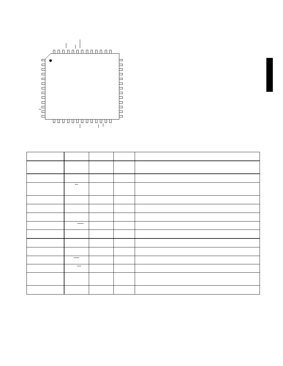
PIN CONNECTIONS
GS7000
TOP VIEW
1
2
3
4
5
6
7
8
9
10
11
12
13
39
38
37
36
35
34
33
32
31
30
29
28
27
52
NC
D
IN0
D
IN1
D
IN2
D
IN3
D
IN4
D
IN5
D
IN6
D
IN7
D
IN8
D
IN9
H
NC
NC
D
OUT0
D
OUT1
D
OUT2
D
OUT3
D
OUT4
D
OUT5
D
OUT6
D
OUT7
D
OUT8
D
OUT9
LOCK
NC
NC
V
EE3
SDO
SDO
V
CC3
CD
SMPTE
NC
NC
PCLK
OUT
V
DD
V
SS
NC
NC
V
EE1
C
1
C
2
V
CC1
SDI
SDI
V
CC2
PCLK
IN
V
EE2
EQ
Rx/Tx
NC
51 50 49 48 47 46 45 44 43 42 41 40
14 15 16 17 18 19 20 21 22 23 24 25 26
PIN DESCRIPTIONS
NUMBER
SYMBOL
TYPE
MODE
DESCRIPTION
1, 13, 14, 26, 27,
39, 40, 44, 45, 52
NC
-
-
No Connect - Connected to Ground.
2-11
D
IN(0,9)
I
Tx
27Mb/s Parallel Data Input
12
H
O
Rx
Indicates the presence of active video. Low after SAV ID and high after
EAV ID
15
V
EE1
-
-
Most negative supply for analog circuits
16, 17
C
1
, C
2
-
-
External 100nF Loop Filter Capacitor Connection
18
V
CC1
-
-
Most positive supply for analog circuits
19, 20
SDI, SDI
I
Rx
Differential Serial Data Input
21
V
CC2
-
-
Most positive supply for PECL circuits
22
PCLK
IN
I
Tx
27MHz External Clock Input
23
V
EE2
-
-
Most negative supply for PECL circuits
24
EQ
I
Rx
Equalizer control. LOW = EQ on, HIGH = EQ bypassed.
25
Rx/Tx
I
-
Receiver/Transmitter Mode Control Input
28
LOCK
O
Rx/Tx
Signal Lock Indication Output. Goes HIGH approximately 38 µs after
valid parallel data occurs.
29 - 38
D
OUT
(9,0)
O
Rx
27Mb/s Parallel Data Output