 | –≠–ª–µ–∫—Ç—Ä–æ–Ω–Ω—ã–π –∫–æ–º–ø–æ–Ω–µ–Ω—Ç: GS7005 | –°–∫–∞—á–∞—Ç—å:  PDF PDF  ZIP ZIP |

GENNUM CORPORATION P.O. Box 489, Stn. A, Burlington, Ontario, Canada L7R 3Y3
Tel. +1 (905) 632-2996 Fax. +1 (905) 632-5946 E-mail: info@gennum.com
www.gennum.com
Revision Date: January 2001
Document No. 522 - 14 - 06
DATA SHEET
G
S
7
005
FEATURES
∑ SMPTE 259M-C compliant
∑ fully integrated 270 Mb/s SDI receiver
∑ integrated cable equalization (100m Belden 8281 typical)
∑ low power consumption (750mW typical)
∑ operates from 0∞C to 85∞C
∑ small footprint with minimal external components
∑ Lock and Carrier Detect output indications
∑ H timing signal output
∑ SMPTE descrambler and NRZI decoder may be
disabled for DVB - ASI applications
∑ ease of design use and adjustment free operation
APPLICATIONS
Limited space, low power SMPTE 259M-C or generic
270Mb/s serial to parallel interfaces; DVB-ASI 270Mb/s
receive interface; broadcast quality uncompressed video
interface for industrial and professional video equipment
such as video editing workstations.
DESCRIPTION
The GS7005 is a BiCMOS integrated circuit capable of
operating as a complete 270Mb/s Serial Digital Video
receiver. The GS7005 provides a complete serial digital
video receive solution while consuming only 750mW.
The serial data input accepts SMPTE 259M-C compliant
signals. An on-chip by-passable equalizer typically pro-
vides 100m of co-axial cable equalization. The clock
recovery is performed on chip with minimal external
components. The incoming serial data is decoded using an
NRZI decoder and SMPTE descrambler to provide SMPTE
125M compliant 27Mb/s parallel data outputs and clock.
BLOCK DIAGRAM
ORDERING INFORMATION
PART NUMBER
PACKAGE
TEMPERATURE
GS7005 - CQT
52 pin MQFP
0∞C to 85∞C
GS7005 - CTT
52 pin MQFP Tape
0∞C to 85∞C
S to P
DESCRAMBLER
TRS
DETECTOR
NRZI
DECODER
f/10
PLL
MUX
SLICER
EQUALIZER
SIGNAL
LOCK
DETECT
SDI
SDI
LOCK
CD
EQ
D
OUT[9:0}
PCLK
OUT
H
C
1
C
2
10
SMPTE
PRO-LINX
TM
GS7005
Complete Serial Digital Video Receiver

GENNUM CORPORATION
522 - 14 - 06
2
G
S
7
005
ABSOLUTE MAXIMUM RATINGS
PARAMETER
VALUE
Supply Voltage
5.5V
Input Voltage Range (any input)
GND < V
IN
< V
CC
DC Input Current (any one input)
10mA
Power Dissipation (V
CC
= 5.25V)
1W
Maximum Die Temperature
125∞C
Operating Temperature Range
0∞C <= T
A
<= 85∞C
Storage Temperature Range
-65∞C <= T
S
<= 150∞C
Lead Temperature (soldering 10s)
260∞C
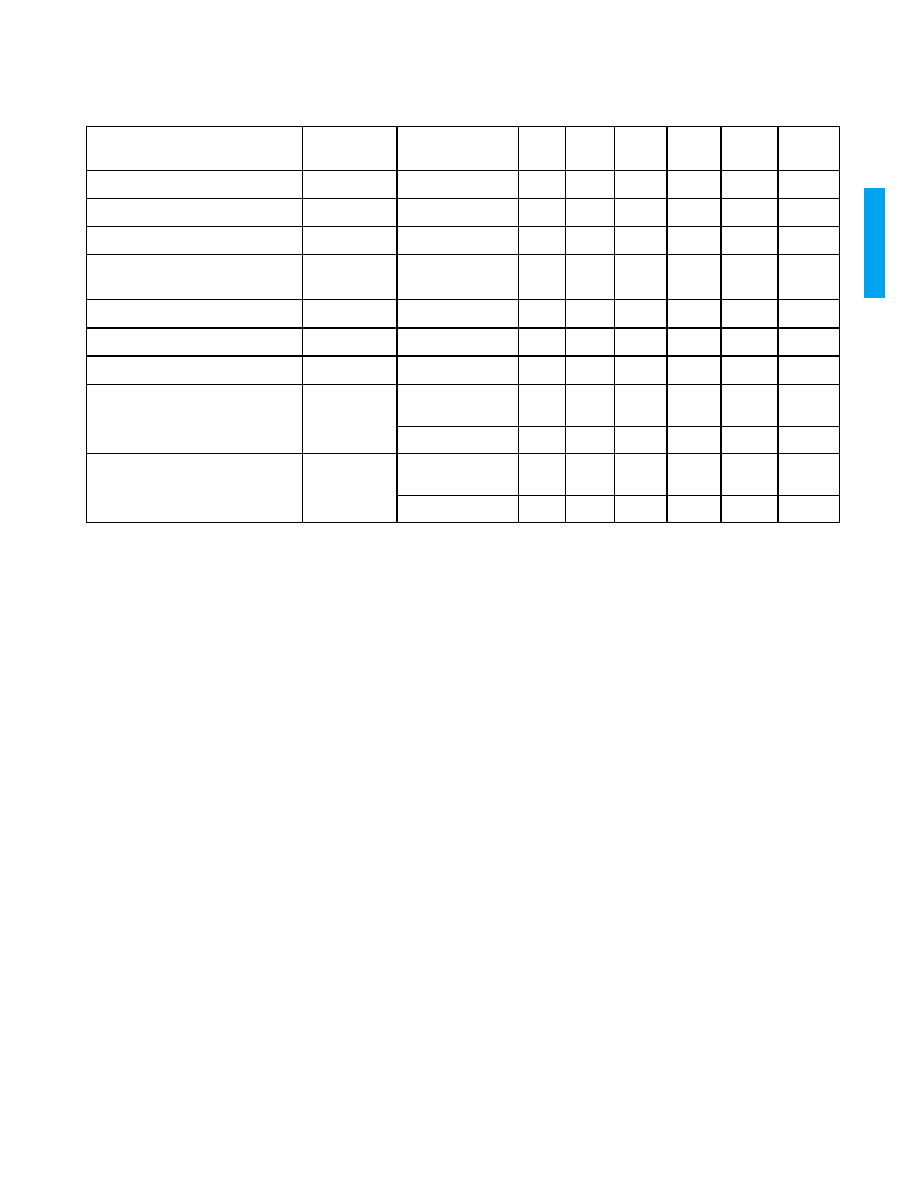
DC ELECTRICAL CHARACTERISTICS
V
CC
= 5V, T
A
= 25∞C, unless otherwise specified.
Serial data rate = 270Mb/s, Parallel Data Rate = 27Mb/s,
PCLK
= 27MHz
PARAMETER
SYMBOL
CONDITIONS
MIN
TYP
MAX
UNITS
NOTES
TEST LEVEL
Positive Supply Voltage
V
CC
Operating
range
4.75
5.00
5.25
V
6
Power Consumption
P
V
CC
= 5.25V
-
750
-
mW
5
Supply Current
I
CC
V
CC
= 5.25V
-
140
-
mA
1
Logic Inputs - Low
V
IL
V
CC
= 5.25V
-
-
0.8
V
6
Logic Inputs - High
V
IH
V
CC
= 4.75V
2
-
-
V
6
Logic Outputs - Low
V
OL
V
CC
= 5.25V
-
-
0.5
V
1
Logic Outputs - High
V
OH
V
CC
= 4.75V
2.4
-
-
V
1
TEST LEVELS
1. Production test at room temperature and nominal supply voltage with guardbands for supply and temperature ranges.
2. Production test at room temperature and nominal supply voltage with guardbands for supply and temperature ranges using
correlated test.
3. Production test at room temperature and nominal supply voltage.
4. QA sample test.
5. Calculated result based on Level 1,2, or 3.
6. Not tested. Guaranteed by design simulations.
7. Not tested. Based on characterization of nominal parts.
8. Not tested. Based on existing design/characterization data of similar product.
GENNUM CORPORATION
522 - 14 - 06
3
G
S
7
005
AC ELECTRICAL CHARACTERISTICS
V
CC
= 5V, T
A
= 25∞C, unless otherwise specified in `conditions'
Serial data rate = 270Mb/s, Parallel Data Rate = 27Mb/s,
PCLK
= 27MHz
PARAMETER
SYMBOL
CONDITIONS
MIN
TYP
MAX
UNITS
NOTE
S
TEST
LEVEL
Parallel Data - Rise/Fall Time
t
R/F_DOUT
C
L
= 20pF
1.0
-
6.0
ns
1
4, 7
PCLK Rising Edge to D
OUT(N)
Centre
t
D
-
-
±5
ns
2, 3
4, 7
PCLK Rise/Fall Time
t
R/F_PCLKOUT
C
L
= 20pF
0.5
-
3.0
ns
1
4, 7
Input Return Loss
LOSS
IN
75
match
5MHz to 270MHz
-
17
-
dB
7
Asynchronous Lock Time
t
LOCK_ASYNC
-
-
250
ms
4
1
Synchronous Lock Time
t
LOCK_SYNC
-
-
10
µs
5
1
Input Jitter Tolerance
t
J_SI
Pathological Input
-
0.35
-
U.I.
6
7
Output PCLK Jitter
t
J_PCLKOUT
Pseudorandom
Input
-
800
-
ps p-p
1
Pathological Input
-
1000
-
ps p-p
6
7
Error Free Cable Length
Pseudorandom
Input
-
100
-
m
7
Pathological Input
75
100
-
m
6, 7
1
NOTES
1. Rise/Fall time is defined as the time for the signal to rise from 20% to 80% of the specified p-p value, or to fall from 80% to 20% of the
specified value.
2. Refer also to Figure 10.
3. This is the time difference between the rising edge of PCLK
OUT
and the centre of the bit period.
4. This is the time delay between a valid serial TRS signal on the input to the moment valid data appears on the parallel outputs.
5. This is the time for the PLL to re-lock when video streams are switched during the vertical blanking interval in accordance with SMPTE
RP168-1993. The two streams may be 180∞ out of phase with respect to one another, but pixel aligned.
6. This pathological pattern is defined in SMPTE RP178-1996, paragraphs 4.1 and 4.3.
7. "Error free" is defined as no single bit errors over a period of 10 minutes, using Belden 8281 Cable and 75
connections. The MIN
value is fully tested and the TYP value is based on using the EB7005 Evaluation Board.
TEST LEVELS
1. Production test at room temperature and nominal supply voltage with guardbands for supply and temperature ranges.
2. Production test at room temperature and nominal supply voltage with guardbands for supply and temperature ranges using correlated
test.
3. Production test at room temperature and nominal supply voltage.
4. QA sample test.
5. Calculated result based on Level 1,2, or 3.
6. Not tested. Guaranteed by design simulations.
7. Not tested. Based on characterization of nominal parts.
8. Not tested. Based on existing design/characterization data of similar product.

GENNUM CORPORATION
522 - 14 - 06
4
G
S
7
005
TEST SETUP
Fig. 1a Test Setup for Jitter Measurements
Fig. 1b Test Setup for Error-Free Cable Length
Fig. 1c Test Setup for Return Loss Measurements
EB7005
BOARD
GS9028
CABLE
DRIVER
TEKTRONIX
TDS 820
SCOPE
TEKTRONIX
GigaBERT
1400
TRANSMITTER
BELDEN 8281
CABLE
DATA
DATA
CLOCK
TRIGGER
EB7005
BOARD
EB9021
EDH ERROR
COUNTER
TEKTRONIX
VIDEO SlGNAL
GENERATOR
BELDEN 8281
CABLE
VIDEO STREAM
WITH EDH
EB7005
BOARD
HP 4195A
NETWORK
ANALYSER
BELDEN 8281
CABLE
GENNUM CORPORATION
522 - 14 - 06
5
G
S
7
005
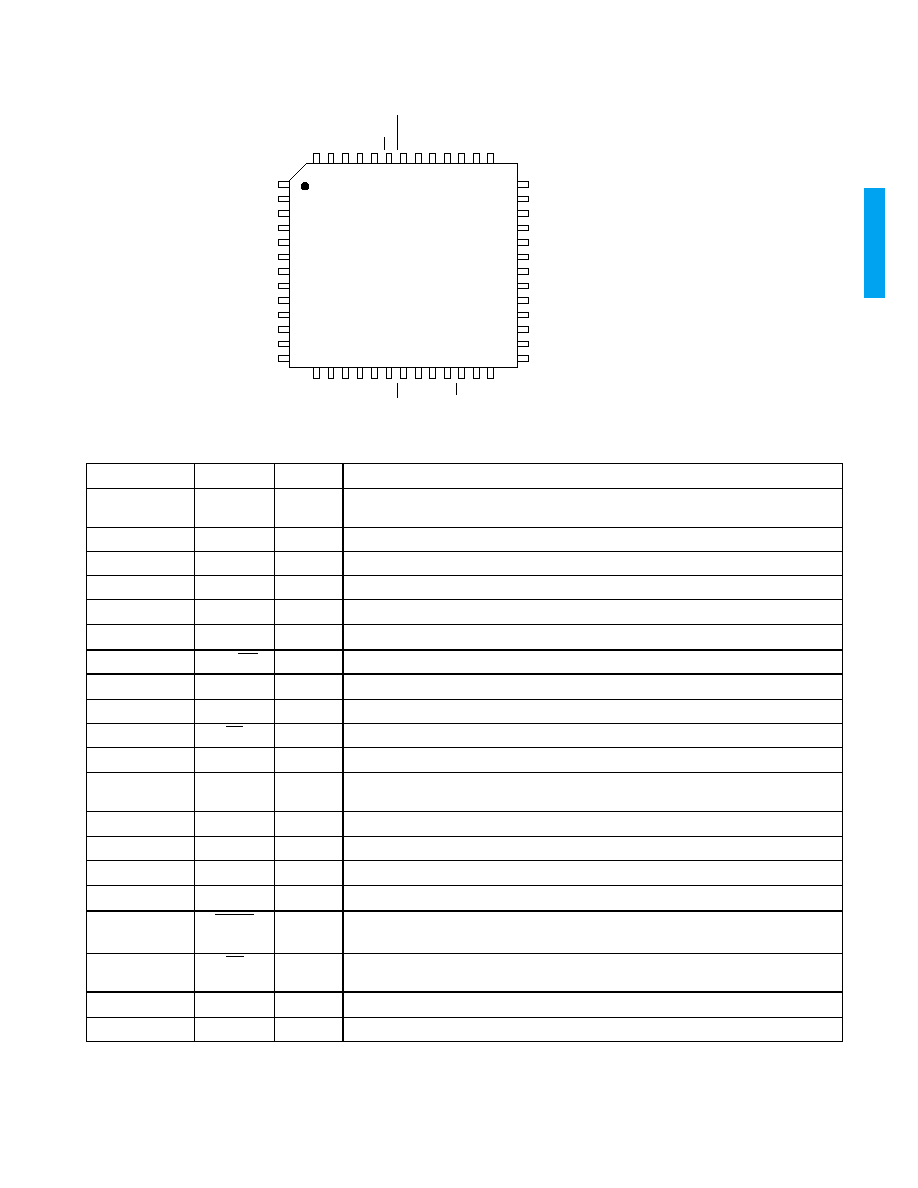
PIN CONNECTIONS
PIN DESCRIPTIONS
NUMBER
SYMBOL
TYPE
DESCRIPTION
1, 13, 14, 26, 27,
39, 40, 52
GND
-
Connect to Ground.
2-11, 22, 44, 45
RSVD0
-
Connect to Ground.
12
H
O
H Indication. HIGH after EAV ID and LOW after SAV ID.
15
GND
-
Ground for analog blocks of the device.
16, 17
C
1
, C
2
-
External 100nF loop filter capacitor connection.
18
V
CC1
-
Power supply for analog blocks of the device.
19, 20
SDI, SDI
I
Differential Serial Data Input
21
V
CC2
-
Power supply for PECL blocks of the device.
23
GND
-
Ground for PECL blocks of the device.
24
EQ
I
Equalizer Control; LOW = EQ on, HIGH = EQ bypassed.
25, 49, 50
RSVD1
-
Connect to V
CC.
28
LOCK
O
Signal Lock Indication Output. Goes HIGH approximately 38µs after valid parallel data
occurs.
29-38
D
OUT[9:0]
O
27Mb/s Parallel Data Outputs.
41
GND
-
Ground for CMOS blocks of the device.
42
V
DD
-
Power supply for CMOS blocks of the device.
43
PCLK
OUT
O
27MHz Clock Output.
46
SMPTE
I
NRZI decoding and descrambling control.
LOW = NRZI and SMPTE mode on. HIGH = NRZI and SMPTE mode disabled.
47
CD
O
Carrier Detect. Active LOW. Goes LOW when carrier is detected and high when carrier is
lost.
48
V
CC3
-
Power supply for Analog and PECL blocks of the device.
51
GND
-
Ground for analog and PECL blocks of the device.
GS7005
TOP VIEW
1
2
3
4
5
6
7
8
9
10
11
12
13
39
38
37
36
35
34
33
32
31
30
29
28
27
14 15 16 17 18 19 20 21 22 23 24 25 26
52 51 50 49 48 47 46 45 44 43 42 41 40
GND
RSVD0
RSVD0
RSVD0
RSVD0
RSVD0
RSVD0
RSVD0
RSVD0
RSVD0
RSVD0
H
GND
GND
D
OUT0
D
OUT1
D
OUT2
D
OUT3
D
OUT4
D
OUT5
D
OUT6
D
OUT7
D
OUT8
D
OUT9
LOCK
GND
GND
GND
RSVD1
RSVD1
V
CC3
CD
SMPTE
RSVD0
RSVD0
PCLK
OUT
V
DD
GND
GND
GND
GND
C
1
C
2
V
CC1
SDI
SDI
V
CC2
RSVD0
GND
EQ
RSVD1
GND
NOTE:
RSVD = Reserved