14583doc3.fm
GENNUM CORPORATION P.O. Box 489, Stn. A, Burlington, Ontario, Canada L7R 3Y3
Tel. +1 (905) 632-2996 Fax. +1 (905) 632-5946 E-mail: info@gennum.com
www.gennum.com
Revision Date: June 2003
Document No. 14583 - 03
DATA SHEET
G
S
7
032
FEATURES
FEATURES
FEATURES
FEATURES
· SMPTE 259M-C compliant (270Mb/s)
· serializes 8-bit or 10-bit data
· minimal external components (no loop filter
components required)
· isolated, dual-output, adjustable cable driver
· 3.3V and 5.0V CMOS/TTL compatible inputs
· lock detect indication
· SMPTE scramble and NRZI coding bypass option
· EDH support with GS9001, GS9021 or EDH FPGA code
APPLICATION
APPLICATION
APPLICATION
APPLICATION
SMPTE 259M-C parallel to serial interfaces for video
cameras, VTRs, signal generators; Generic parallel to serial
conversion.
DESCRIPTION
DESCRIPTION
DESCRIPTION
DESCRIPTION
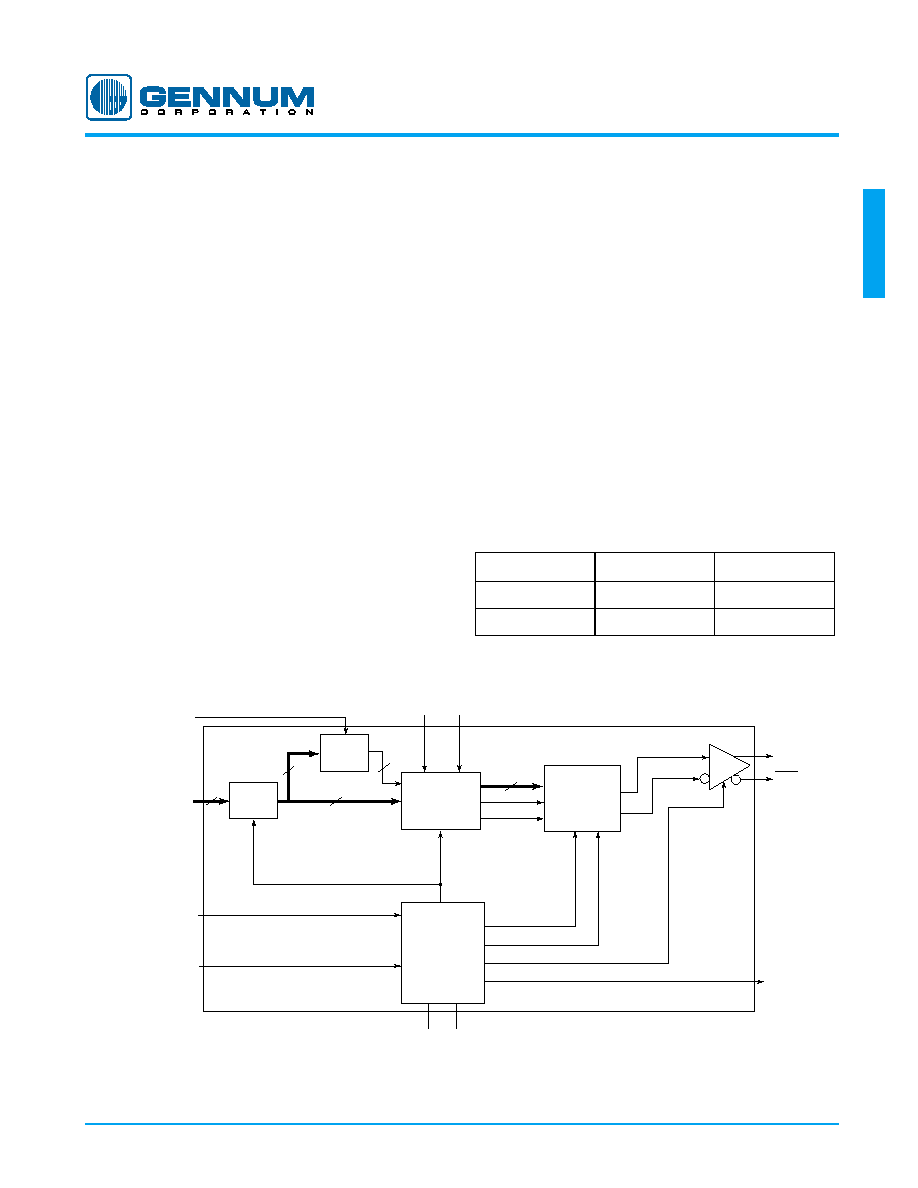
The GS7032 is designed to encode and serialize SMPTE
125M bit parallel digital video signals as well as other 8-bit
or 10-bit parallel formats. This device performs the following
functions:
·
sync detection
·
parallel to serial conversion
·
data scrambling (using the X
9
+ X
4
+ 1 algorithm)
·
10x parallel clock multiplication
·
conversion of NRZ to NRZI serial data
The GS7032 features 270M/bs data rate with a single VCO
resistor. Other features include a lock detect output, NRZI
encoding and SMPTE scrambler bypass, a sync detect
disable, and an isolated dual output cable driver suitable
for driving 75
loads.
BLOCK DIAGRAM
BLOCK DIAGRAM
BLOCK DIAGRAM
BLOCK DIAGRAM
ORDERING INFORMATION
ORDERING INFORMATION
ORDERING INFORMATION
ORDERING INFORMATION
PART NUMBER
PACKAGE
TEMPERATURE
GS7032 - CVM
44 pin TQFP
0°C to 70°C
GS7032 - CTM
44 pin TQFP Tape
0°C to 70°C
LOCK
DETECT
(LOCK DET)
SERIAL
DIGITAL
OUTPUTS
PARALLEL CLOCK
INPUT (PCLKIN)
P
LOAD
S
CLK
S
CLK
/10
LOOP BANDWIDTH
CONTROL (LBWC)
R
VCO+
R
VCO-
MUTE
RESET
RESET
SYNC DETECT DISABLE (SYNC DIS)
BYPASS
BYPASS
PARALLEL
to SERIAL
CONVERTER
&
NRZ to NRZI
DATA
IN
(PD0-PD9)
10
10
8
INPUT
LATCH
2
10
SYNC
DETECT
SMPTE
SCRAMBLER
PLL
SDO
SDO
352/,1;
TM
GS7032
GS7032
GS7032
GS7032
Digital Video Serializer
Digital Video Serializer
Digital Video Serializer
Digital Video Serializer
GENNUM CORPORATION
14583 - 03
2 of 9
G
S
7
032
ABSOLUTE MAXIMUM RATINGS
ABSOLUTE MAXIMUM RATINGS
ABSOLUTE MAXIMUM RATINGS
ABSOLUTE MAXIMUM RATINGS
PARAMETER
VALUE
Supply Voltage (V
S
= V
CC
-V
EE
)
5.5V
Input Voltage Range (any input)
V
EE
<V
IN
<V
CC
DC Input Current (any one input)
5mA
Power Dissipation (V
CC
= 5.25V)
1200mW
j-a
42.5°C/W
j-c
6.4°C/W
Maximum Die Temperature
125°C
Operating Temperature Range
0°C
T
A
70°C
Storage Temperature Range
-65°C
T
S
150°C
Lead Temperature (soldering, 10 sec)
260°C
DC ELECTRICAL CHARACTERISTICS
DC ELECTRICAL CHARACTERISTICS
DC ELECTRICAL CHARACTERISTICS
DC ELECTRICAL CHARACTERISTICS
V
CC
= 5V, V
EE
= 0V, T
A
= 0° 70°C unless otherwise specified.
PARAMETER
SYMBOL
CONDITIONS
MIN
TYP
MAX
UNITS
NOTES
TEST
LEVEL
Positive Supply Voltage
V
CC
Operating Range
4.75
5.00
5.25
V
3
Power (System Power)
P
V
CC
= 5.0V, T = 25°C (2 outputs)
-
550
-
mW
5
Supply Current
CC
V
CC
= 5.25V (2 outputs)
-
-
160
mA
1
V
CC
= 5.0V, T = 25°C (2 outputs)
-
110
-
mA
3
Data & Clock Inputs
(PD[9:0] PCLKIN)
SYNC DIS
V
IH
Logic Input High (wrt V
EE
)
2.4
-
-
V
3
V
IL
Logic Input Low (wrt V
EE
)
-
-
0.8
V
L
Input Current
-
-
8.0
µA
Logic Input Levels
(Bypass, RESET)
V
IH
Logic Input High (wrt to V
EE
)
2.4
-
-
V
3
V
IL
Logic Input Low (wrt to V
EE
)
-
-
0.8
V
L
Input Current
-
-
5.0
µA
Lock Detect Output
V
OL
Sinking 500µA
-
-
0.4
V
1
TEST LEVELS
1. Production test at room temperature and nominal supply voltage with guardbands for supply and temperature ranges.
2. Production test at room temperature and nominal supply voltage with guardbands for supply and temperature ranges using correlated
test.
3. Production test at room temperature and nominal supply voltage.
4. QA sample test.
5. Calculated result based on Level 1,2, or 3.
6. Not tested. Guaranteed by design simulations.
7. Not tested. Based on characterization of nominal parts.
8. Not tested. Based on existing design/characterization data of similar product.
GENNUM CORPORATION
14583 - 03
3 of 9
G
S
7
032
AC ELECTRICAL CHARACTERISTICS
AC ELECTRICAL CHARACTERISTICS
AC ELECTRICAL CHARACTERISTICS
AC ELECTRICAL CHARACTERISTICS
V
CC
= 5V, V
EE
= 0V, T
A
= 0° 70°C unless otherwise specified.
PARAMETER
SYMBOL
CONDITIONS
MIN
TYP
MAX
UNITS
NOTES
TEST
LEVEL
Serial Data Bit Rate
BR
SDO
R
VCO
= 374
-
270Mb/s
-
Mb/s
SMPTE
259M-C
3
Serial Data Outputs Signal
Swing
V
SDO
R
LOAD
= 37.5
, R
SET
= 54.9
740
800
860
mVp-p
1
SD Rise/Fall Times
t
r
, t
f
20% - 80%
400
-
700
ps
7
SD Overshoot/Undershoot
-
-
7
%
1
7
Output Return Loss
O
RL
at 270MHz
15
-
-
dB
1
7
Lock Time
t
LOCK
Worst case
-
-
5
ms
6
Min Loop Bandwidth
BW
MIN
LBWC = Grounded : BW
MIN
-
220
-
kHz
7
Typical Loop Bandwidth
BW
TYP
LBWC = Floating :
BW
MIN
-
500
-
kHz
7
Max Loop Bandwidth
BW
MAX
LBWC = V
CC
: 10 BW
MIN
-
1.7
-
MHz
7
Intrinsic Jitter (6
)
LBWC = V
CC
(270Mb/s)
-
0.08
-
UI
3
Data & Clock Inputs
(PD[9:0] PCLKIN)
t
SU
Setup Time at 25°C
2.5
-
-
ns
3
t
H
Hold Time at 25°C
2.0
-
-
ns
3
TEST LEVELS
1. Production test at room temperature and nominal supply voltage with guardbands for
supply and temperature ranges.
2. Production test at room temperature and nominal supply voltage with guardbands for
supply and temperature ranges using correlated test.
3. Production test at room temperature and nominal supply voltage.
4. QA sample test.
5. Calculated result based on Level 1,2, or 3.
6. Not tested. Guaranteed by design simulations.
7. Not tested. Based on characterization of nominal parts.
8. Not tested. Based on existing design/characterization data of similar product.
NOTES
1. Depends on PCB layout.
10
GENNUM CORPORATION
14583 - 03
4 of 9
G
S
7
032
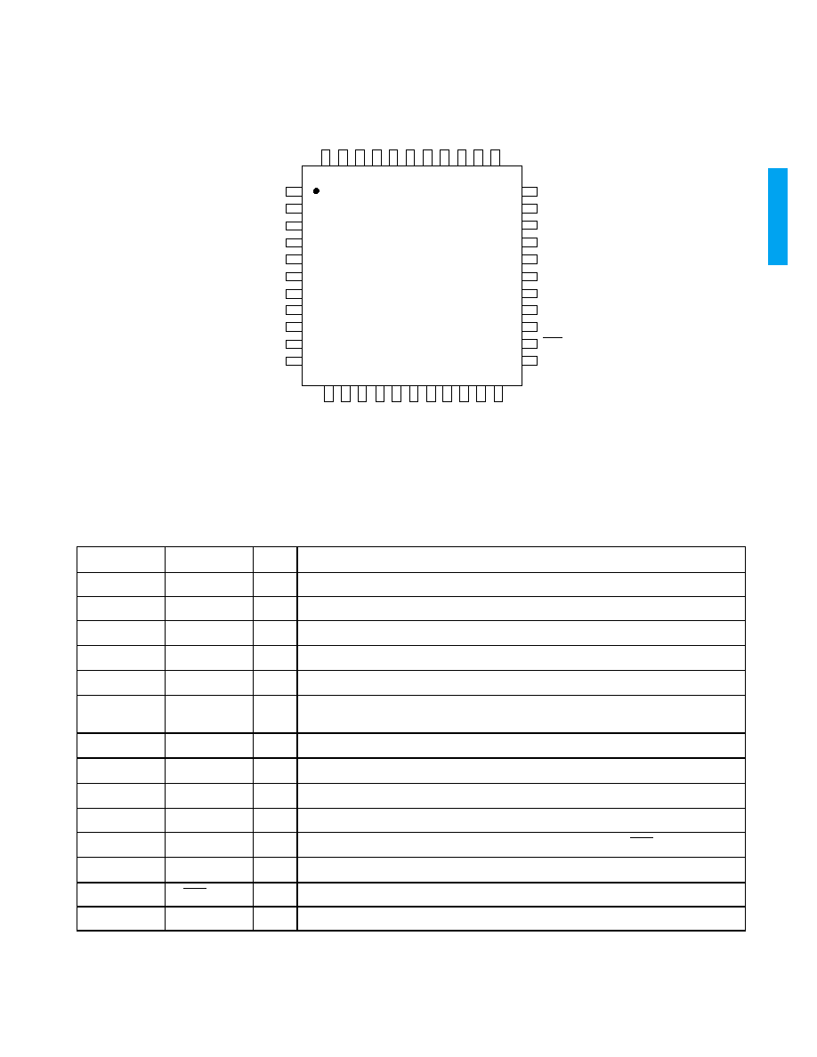
PIN CONNECTIONS
PIN CONNECTIONS
PIN CONNECTIONS
PIN CONNECTIONS
GS7032
TOP VIEW
44 43 42 41 40 39 38 37 36 35 34
R
VCO+
LF+
V
EE
R
VCO-
LF-
V
CC1
LBWC
NC
SYNC DIS
V
EE
V
EE1
33
32
31
30
29
28
27
26
25
24
23
NC
BYPASS
NC
V
EE
NC
NC
V
EE
SDO
SDO
V
EE
PD9
PD8
PD7
PD6
PD5
PD4
PD3
PD2
PD1
PD0
PCLKIN
1
2
3
4
5
6
7
8
9
10
11
12 13 14 15 16 17 18 19 20 21 22
V
CC2
V
EE
2
RSV2
R
SET
RSV1
NC
NC
LOCK
V
EE3
NC
V
CC3
RESET
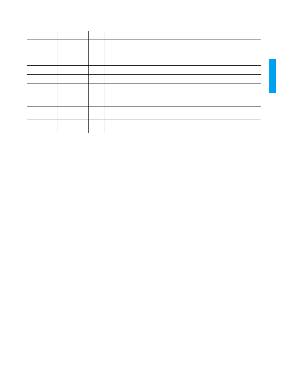
PIN DESCRIPTIONS
PIN DESCRIPTIONS
PIN DESCRIPTIONS
PIN DESCRIPTIONS
NUMBER
SYMBOL
TYPE
DESCRIPTION
1-10
PD9 - PD0
I
CMOS or TTL compatible parallel data inputs. PD0 is the LSB and PD9 is the MSB.
11
PCLKIN
I
CMOS or TTL compatible parallel clock input.
12
V
EE3
-
Most negative power supply connection for parallel data and clock inputs.
13
V
CC3
-
Most positive power supply connection for parallel data and clock inputs.
14
RSV2
I
Reserved pin. Do not connect.
15, 19, 21, 27,
28, 30, 32, 37
NC
I
No connect.
16
RSV1
I
Reserved pin. Always connect to V
CC
.
17
V
CC2
-
Most positive power supply connection for internal logic and digital circuits.
18
V
EE2
-
Most negative power supply connection for internal logic and digital circuits.
20
LOCK
O
TTL level which is high when the internal PLL is locked.
22
R
SET
I
External resistor used to set the data output amplitude for SDO and SDO.
23, 26, 29
V
EE
-
Most negative power supply connection for shielding (not connected).
24, 25
SDO, SDO
O
Primary, current mode, 75
cable driving output (inverse and true)
31
BYPASS
I
When high, the SMPTE Scrambler and NRZ encoder are bypassed.
GENNUM CORPORATION
14583 - 03
5 of 9
G
S
7
032
33
RESET
I
Resets the scrambler when asserted.
34
V
CC1
-
Most positive power supply connection for analog circuits.
35
V
EE1
-
Most negative power supply connection for analog circuits.
36, 38
R
VCO
+, R
VCO
-
I
Differential VCO current setting resistor that sets the VCO frequency.
39, 43
V
EE
-
Most negative power supply connection (substrate).
40
LBWC
I
TTL level loop bandwidth control that adjusts the PLL bandwidth to optimize for lowest
jitter. If the pin is set to ground the loop bandwidth is BW
MIN
. If the pin is left floating, the
loop bandwidth is approximately 3 BW
MIN
, if the pin is tied to V
CC
the loop bandwidth is
approximately10 BW
MIN
41, 42
LF+, LF-
I
Differential loop filter pins to optimize loop transfer performance at low loop bandwidths
(NC if not used).
44
SYNC DIS
I
Sync detect disable. Logic high disables sync detection. Logic low allows 8 bit operation
by mapping 000-003 to 000 and 3FC-3FF to 3FF.
PIN DESCRIPTIONS
PIN DESCRIPTIONS
PIN DESCRIPTIONS
PIN DESCRIPTIONS
NUMBER
SYMBOL
TYPE
DESCRIPTION