GENLINX
TM
GS9002A
Serial Digital Encoder
DATA SHEET
FEATURES
DEVICE DESCRIPTION
The GS9002A is a monolithic bipolar integrated circuit
designed to serialize SMPTE 125M and SMPTE 244M bit
parallel digital signals as well as other 8 or 10 bit parallel
formats. This device performs the functions of sync detection,
parallel to serial conversion, data scrambling (using the X
9
+
X
4
+1 algorithm), 10x parallel clock multiplication and
conversion of NRZ to NRZI serial data. It supports any of four
selectable serial data rates from 100 Mb/s to over 360 Mb/s.
The data rates are set by resistors and are selected by an
on-board 2:4 decoder having two TTL level input address
lines.
Other features such as a sync detector output, a sync detector
disable input, and a lock detect output are also provided. The
X
9
+ X
4
+ 1 scrambler and NRZ to NRZI converter may be
bypassed to allow the output of the parallel to serial converter
to be directly routed to the output drivers.
The GS9002A provides pseudo-ECL outputs for the serial
data and serial clock as well as a single-ended pseudo-ECL
output of the regenerated parallel clock.
The GS9002A directly interfaces with cable drivers GS9007A,
GS9008A and GS9009A. The device requires a single +5 volt
or -5 volt supply and typically consumes 713 mW of power
while driving 100
loads. The 44 pin PLCC packaging
assures a small footprint for the complete encoder function.
� fully compatible with SMPTE-259M serial digital
standard
� supports up to four serial bit rates to 400 Mb/s
� accepts 8 bit and 10 bit TTL and CMOS
compatible parallel data inputs
� X
9
+ X
4
+ 1 scrambler, NRZI converter and sync
detector may be disabled for transparent data
transmission
� pseudo-ECL serial data and clock outputs
� single +5 or -5 volt supply
� 713 mW typical power dissipation (including ECL
pull-down loads).
� 44 pin PLCC packaging
� Pb-free and Green
APPLICATIONS
� 4
SC
, 4:2:2 and 360 Mb/s serial digital interfaces for
Video cameras, VTRs, Signal generators
ORDERING INFORMATION
Revision Date: June 2004
FUNCTIONAL BLOCK DIAGRAM
Patent No.5,357,220
GENNUM CORPORATION P.O. Box 489, Stn A, Burlington, Ontario, Canada L7R 3Y3 tel. (905) 632-2996 fax: (905) 632-5946
Gennum Japan: Shinjuku Green Tower Building 27F 6-14-1, Nishi Shinjuku Shinjuku-ku, Tokyo 160-0023 Japan Tel: +81 (03) 3349-5501 Fax: +81 (03) 3349-5505
Document No. 24149 - 1
SYNC DETECT
DISABLE
GS9002A
PLD
LOOP FILTER
RVC00
RVC01
RVC02
RVC03
LOCK DETECT
SERIAL CLOCK
SYNC DETECT
PCLK IN
PARALLEL DATA
IN (10 BITS)
P/S
CONVERTER
PCLK OUT
DRS1
DRS0
SYNC
DETECT
DATA RATE
SWITCH
REGULATOR CAP
PHASE
FREQUENCY
DETECT
CHARGE
PUMP
VCO
INPUT
LATCH
DIV BY 10
GENERATOR
6
7-16
17
22
19
3
20
43
29
36
32
33
35
31
34
26
SCRAMBLER/
SERIALIZER
SELECT
SCLK
LOCK
DETECT
NRZ
NRZI
2:1 MUX
SERIAL CLOCK
42
SCRAMBLER
SERIAL DATA
SERIAL DATA
39
38
NOT RECOMMENDED FOR NEW DESIGNS
Part Number
Package
Temperature Pb-Free and Green
GS9002ACPM
44 Pin PLCC
o�C to 70�C
No
GS9002ACPME3
44 Pin PLCC
o�C to 70�C
Yes
2 of 11
24149 - 1
NOT RECOMMENDED FOR NEW DESIGNS
PARAMETER SYMBOL
CONDITIONS
MIN
TYP
MAX UNITS NOTES
Supply Voltage
V
S
Operating Range
4.75
5.0
5.25
V
Power Consumption
P
D
SDO/SDO connected to (V
CC
-2V)
thru 100� resistors, PCK OUT
-
690
870
mW
connected to V
EE
via 1k
Same as above with SCK/SCK
-
710
900
mW
also connected to (V
CC
-2V)
thru 100
resistors.
Supply Current
I
S
SDO/SDO connected to (V
CC
-2V)
-
155
190
mA
thru 100� resistors, PCK OUT
connected to V
EE
via 1k
Same as above with SCK/SCK
to (V
CC
-2V) V thru 100
resistors.
-
170
205
mA
see Figure 15
TTL Inputs-HIGH
V
IHmin
T
A
= 25�C
2.0
-
-
V
TTL Inputs-LOW
V
ILmax
T
A
= 25�C
-
-
0.8
V
Logic Input Current
I
INmax
-
2.5
10
�A
TTL Outputs-HIGH
V
OHmin
T
A
= 25�C
2.4
-
-
V
TTL Outputs-LOW
V
OLmax
T
A
= 25�C
-
-
0.5
V
Sync Detect O/P
I
OSYNC
-
-
4.0
mA
SINK & SOURCE
Serial Outputs High
V
OH
T
A
=25�C, R
L
=100
to V
CC
-2V -0.875
-
-0.7
V
(SDO & SCK) Low
V
OL
(
V
CC
-2V
)
-1.8
-
-1.5
V
Serial Data Outputs
bit rates
BR
SDO
R
L
= 100
to
100
-
400
Mb/s
(
VCC-2 volts
)
signal swing
V
SDO
700
850
1000
mV p-p
rise/fall times
t
R
, t
F
-
500
-
ps
20% - 80%
jitter
t
J(SDO)
143 Mb/s
-
400
-
ps p-p
see Note 1
270 Mb/s
-
300
-
ps p-p
see Fig. 16
Serial Clock Outputs
frequency
SCK
R
L
= 100
to
100
-
400
MHz
see Fig. 12, 13
(
VCC-2 volts
)
signal swing
V
SCK
-
800
-
mV p-p
see Fig. 14
Serial Data to Clock Timing
t
D
See Figure 9
-
1.4
-
ns
Data lags Clock
Lock Time
t
LOCK
C
LOOP FILT
= 0.1�F
-
1
1.2
ms
R
LOOP FILT
= 3.9k
Parallel Clock Output
frequency
PCKO
R
L
= 1k
to V
EE
10
-
40
MHz
PCKO
=
SCK
/10
signal swing
V
PCKO
-
800
-
mV p-p
rise/fall times
t
R
, t
F
-
700
-
ps
20% - 80%
jitter
t
JPCKO
-
400
-
ps p-p
Parallel Data & Clock Inputs
risetime
t
R
T
A
= 25�C
500
-
-
ps
setup
t
SU
3
-
-
ns
hold
t
HOLD
3
-
-
ns
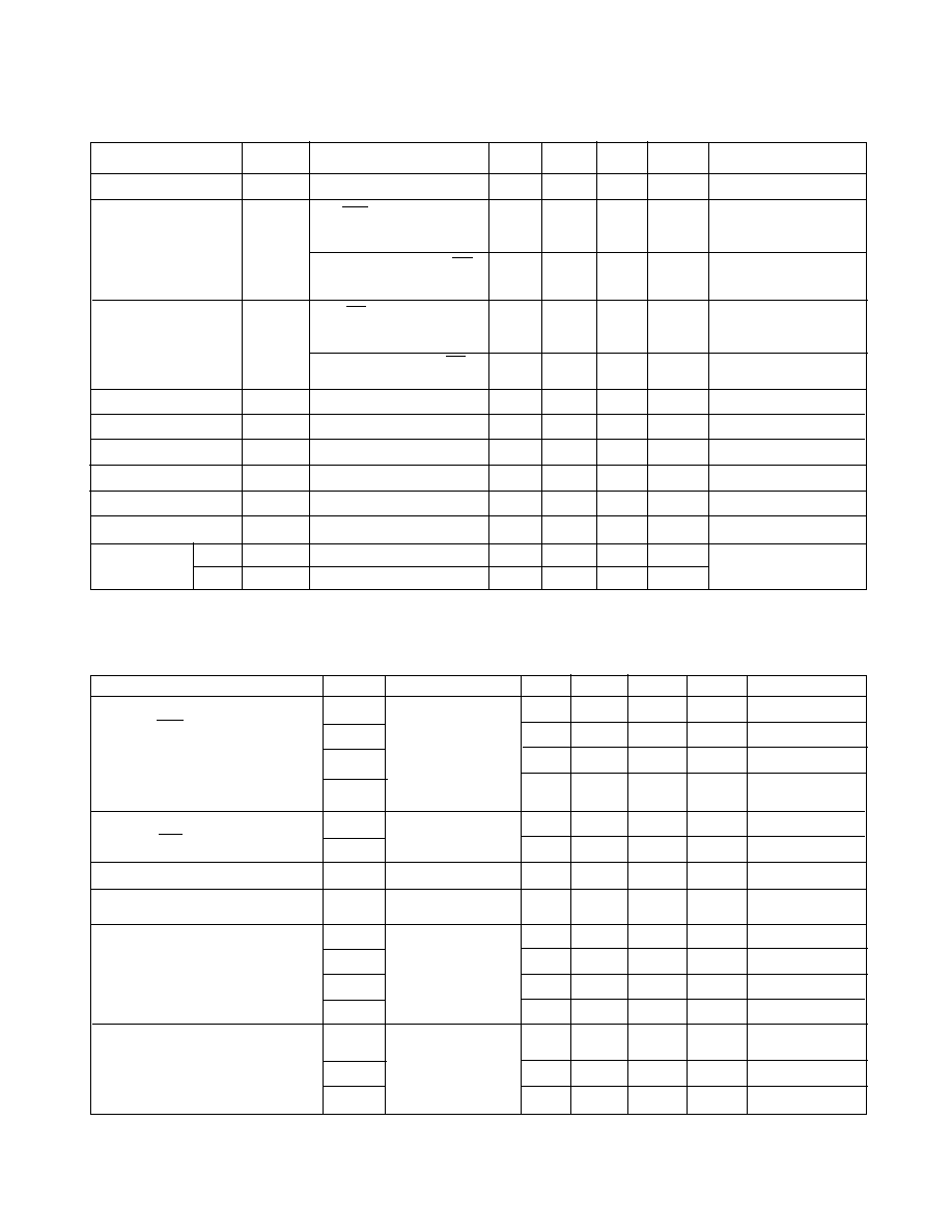
NOTE 1: Measured using PCK-IN as trigger source on 1GHz analog oscilloscope.
V
CC
= 5V, V
EE
= 0V, T
A
= 0�C
to 70�C unless otherwise shown
GS9002A - ENCODER DC ELECTRICAL CHARACTERISTICS
GS9002A - ENCODER AC ELECTRICAL CHARACTERISTICS
V
CC
= 5V, V
EE
= 0V, T
A
= 0�C
to 70�C, V
LOOP FILTER
=2.6 V unless otherwise shown,
T
A
= 25�C
with respect to V
CC
(SDO and SDO)
(SCK and SCK)
(PCK OUT)
PARAMETER
SYMBOL CONDITIONS MIN TYP MAX UNITS NOTES

3 of 11
24149 - 1
NOT RECOMMENDED FOR NEW DESIGNS
ABSOLUTE MAXIMUM RATINGS
PARAMETER
VALUE/UNITS
Supply Voltage
5.5 V
Input Voltage Range (any input)
-V
EE
< V
I
< V
CC
DC Input Current (any one input)
10 mA
Power Dissipation (V
S
= 5.25 V)
1 W
Operating Temperature Range
0
�
C
T
A
70
�
C
Storage Temperature Range
-65
�
C
T
S
150
�
C
Lead Temperature (soldering 10 seconds)
260
�
C
Fig. 1 GS9002A Encoder Pin Connections
SDO
SDO
V
EE
DRS0
DRS1
RVC00
RVC01
RVC02
RVC03
V
EE
C. REG
SYNC
DET.
DIS.
V
CC1
V
EE
SYNC
DET.
V
CC3
V
EE
V
EE
SCK
SCK
V
CC2
a
V
CC2
b
V
CC3
V
EE
NC
V
EE
LOOP
FILT.
V
CC3
LOCK
DET.
PCK
OUT
V
EE
PD0
PD1
PD2
PD3
PD4
PD5
PD6
PD7
PD8
PD9
PCK IN
PARALLEL
DATA
INPUTS
VCO
FREQUENCY
SET
RESISTORS
GS9002A
TOP VIEW
39
38
37
36
35
34
33
32
31
30
29
7
8
9
10
11
12
13
14
15
16
17
18 19 20 21 22 23 24 25 26 27 28
6 5 4 3 2 44 43 42 41 40
SSS
V
EE
4 of 11
24149 - 1
NOT RECOMMENDED FOR NEW DESIGNS
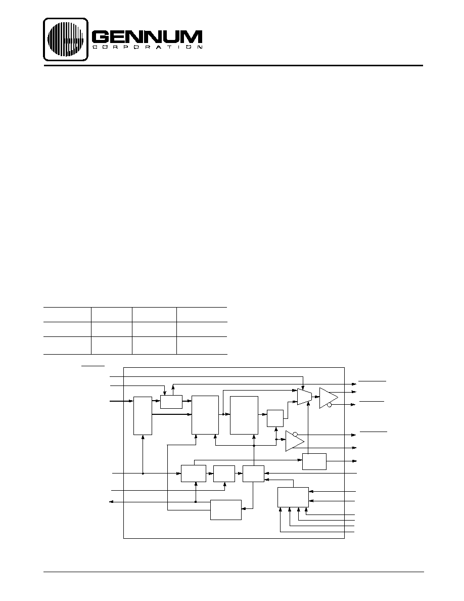
The GS9002A Encoder is a bipolar integrated circuit used to
convert parallel data into a serial format according to the
SMPTE 259M standard. The device encodes both eight and
ten bit TTL-compatible parallel signals producing serial data
rates up to 400 Mb/s. It operates from a single five volt supply
and is packaged in a 44 pin PLCC.
Functional blocks within the device include the input latches,
sync detector, parallel to serial converter, scrambler, NRZ to
NRZ
I converter, ECL output buffers for data and clock, PLL for
10x parallel clock multiplication and lock detect.
The parallel data (PD0-PD9) and parallel clock (PCK-IN) are
applied via pins 7 through 17 respectively.
Sync Detector
The Sync Detector looks for the reserved words 000-003 and
3FC-3FF, in ten bit Hex, or 00 and FF in eight bit Hex, used in
the TRS-ID sync word. When the occurrence of either all zeros
or ones at inputs PD2-PD9 is detected, the lower two bits PD0
and PD1 are forced to zeros or ones, respectively. This makes
the system compatible with eight or ten bit data. For non -
SMPTE standard parallel data, a logic input, Sync Disable (6)
is available to disable this feature.
Scrambler
The Scrambler is a linear feedback shift register used to
pseudo-randomize the incoming serial data according to the
fixed polynomial (X
9
+X
4
+1). This minimizes the DC component
in the output serial data stream. The NRZ to NRZI converter
uses another polynomial (X+1) to convert a long sequence of
ones to a series of transitions, minimizing polarity effects.
GS9002A Serial Digital Encoder - Detailed Device Description
Phase Locked Loop
The PLL performs parallel clock multiplication and provides
the timing signal for the serializer. It is composed of
a phase/frequency detector, charge pump, VCO and a
divide-by-ten counter.
The phase/frequency detector allows a wider capture range
and faster lock time than that which can be achieved with a
phase discriminator alone. The discrimination of frequency
also eliminates harmonic locking. With this type of discriminator,
the PLL can be over-damped for good stability without
sacrificing lock time.
The charge pump delivers a 'charge packet' to the loop filter
which is proportional to the system phase error. Internal
voltage clamps are used to constrain the loop filter voltage
between approximately 1.8 and 3.4 volts.
The VCO, constructed from a current-controlled multivibrator,
features operation in excess of 400 Mb/s and a wide pull range
(
�40% of centre frequency).
VCO Centre Frequency Selection
The wide VCO pull range allows the PLL to compensate for
variations in device processing, temperature variations and
changes in power supply voltage, without external adjustment.
A single external resistor is used to set the VCO current for
each of four centre frequencies as selected by a two bit code
through a 2:4 decoder.
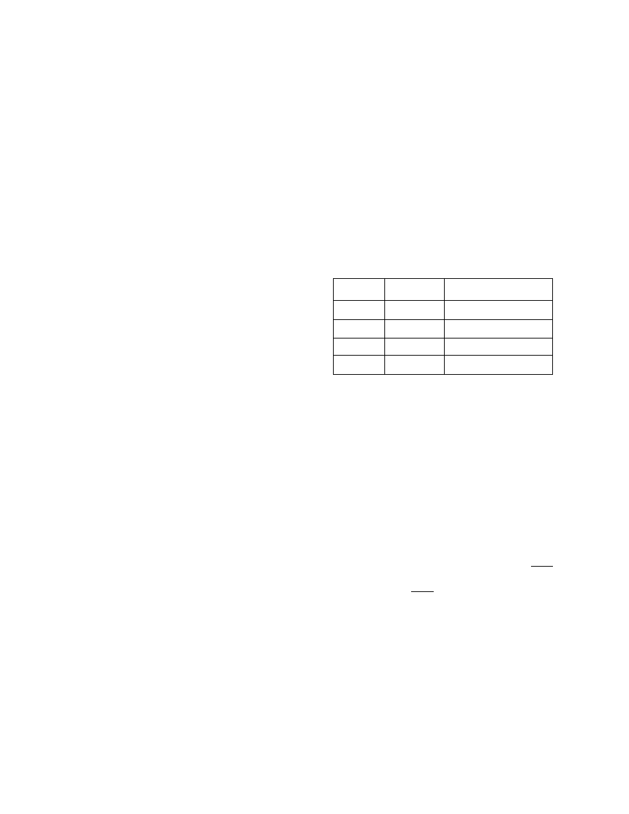
The current setting resistors are connected to the RVCO0
through RVCO3 inputs (34, 33, 32 and 31). The decoder
inputs DRS0 and DRS1 (36, 35) are TTL compatible inputs
and select the four resistors according to the following truth
table.
DRS1
DRS0
Resistor Selected
0
0
RVCO0 (34)
0
1
RVCO1 (33)
1
0
RVCO2 (32)
1
1
RVCO3 (31)
A 2:1 multiplexer (MUX) selects either the direct data from the
P/S Converter (Serializer) or the NRZI data from the Scrambler.
This MUX is controlled by the Scrambler/Serializer Select
(SSS) input pin 26. When this input is LOW the MUX selects
the Scrambler output. (This is the mode used for SMPTE
259M data). When this input is HIGH the MUX directly routes
the serialized data to the output buffer with no scrambling or
NRZ to NRZ
I
conversion.
The lock detect circuit disables the serial data output when the
loop is not locked by turning off the 2:1 MUX. The Lock Detect
output is available from pin 20 and is HIGH when the loop is
locked.
The true and complement serial data, SDO and SDO are
available from pins 38 and 39 while the true and complement
serial clock, SCK and SCK are available from pins 43 and 42
respectively. If the serial clock is not used pins 43 and 42 can
be connected to V
CC
.
The regenerated parallel clock (PCK OUT) is available at pin
19. This output is a single ended pseudo-ECL output requiring
a pull down resistor. If regenerated parallel clock is not used
pin 19 can be connected to V
CC
.

5 of 11
24149 - 1
NOT RECOMMENDED FOR NEW DESIGNS
GS9002A PIN DESCRIPTIONS
PIN NO.
SYMBOL TYPE
DESCRIPTION
1
V
EE
Power Supply: Most negative power supply connection.
2
V
CC3
Power Supply: Most positive power supply connection for the PLL and scrambler.
3
SYNC DET.
O
TTL output level that detects the occurrence of all zero's or all one's at inputs PD2-PD9
and pulses LOW for three PCK-IN durations. Used to detect SMPTE 259M reserved words
(000-003 and 3FC-3FF) in TRS sync word. Parallel data bits PD0 and PD1 are set Low or
High when PD2 - PD9 are Low or High respectively.
4
V
EE
Power Supply: Most negative power supply connection.
5
V
CC1
Power Supply: Most positive power supply connection for the input data latches and serializer.
6
SYNC DET.
I
TTL level input that disables the internal Sync Detector when HIGH. This allows the
DISABLE
GS9002 to serialize 8 or 10 bit non - SMPTE Standard parallel data.
7-16
PD0-PD9
I
TTL level inputs of the parallel data words. PD0 is the LSB and PD9 is the MSB.
17
PCK-IN
I
TTL level input of the Parallel Clock.
18
V
EE
Power Supply: Most negative power supply connection.
19
PCK OUT
O
Pseudo-ECL output representing the re-clocked Parallel Clock and is derived from the
internal VCO. The VCO is divided by 10 in order to produce this output.
20
LOCK DET.
O
TTL level output which goes HIGH when the internal PLL is locked.
21
V
CC3
Power Supply: Most positive power supply connection for the PLL and scrambler.
22
LOOP FILT.
I
Connection for the R-C loop filter components. The loop filter sets the PLL loop
parameters.
23
V
EE
Power Supply: Most negative power supply connection.
24
NC
25
V
EE
Power Supply: Most negative power supply connection.
26
SSS
I
Scrambler/Serializer Select. TTL level input that selects scrambled NZRI output when
logic LOW or direct serializer output when logic HIGH.
27
V
EE
Power Supply: Most negative power supply connection.
28
V
CC3
Power Supply: Most positive power supply connection for the PLL and scrambler.
29
C
REG
I
Compensation RC network for internal voltage regulator that requires decoupling with a series
0.1�F capacitor and 820
resistor. Components should be located as close as possible to the pin.
30
V
EE
Power Supply: Most negative power supply connection.
31
R
VCO3
I
VCO Resistor 3: Analog current input used to set the centre frequency of the VCO when
the two Data Rate Select bits (pins 35 and 36) are both set to logic 1. A resistor is
connected from this pin to V
EE
.
32
R
VCO2
I
VCO Resistor 2: Analog current input used to set the centre frequency of the VCO when
the Data Rate Select Bit 0 (pin 36) is set to logic 0 and the Data Rate Select Bit 1 (pin 35)
is set to logic 1. A resistor is connected from this pin to V
EE
.
33
R
VCO1
I
VCO Resistor 1: Analog current input used to set the centre frequency of the VCO when
the Data Rate Select Bit 0 (pin 36) is set to logic 1 and the Data Rate Select Bit 1 (pin 35)
is set to logic 0. A resistor is connected from this pin to V
EE
.
34
R
VCO0
I
VCO Resistor 0: Analog current input used to set the centre frequency of the VCO when
the two Data Rate Select bits (pins 35 and 36) are both set to logic 0. A resistor is
connected from this pin to V
EE
.
35,36
DRS0, 1
I
TTL level inputs to the internal 2:4 demultiplexer used to select one of four VCO frequency
setting resistors (R
VCO0
- R
VCO3
). (See above)