
NOT RECOMMENDED
FOR NEW DESIGNS
Part Number Package Type Temperature Range
Pb-Free and Green
GS9004DCKB 14 pin SOIC
0
o
C to 70
o
C
No
GS9004DCTB 14 pin SOIC Tape
0
o
C to 70
o
C
No
GS9004DCKBE3 14 pin SOIC
0
o
C to 70
o
C
Yes
FEATURES
∑
automatic cable equalization
∑
typically greater than 300 m of high quality cable at
270 Mb/s
∑
typically 300 m of high quality cable at 360 Mb/s
∑
drop in replacement for GS9004C
∑
capability to drive 50
W
loads (to V
TT
)
∑
fully compatible with SMPTE 259M and operational to
400 Mb/s
∑
signal strength indicator
∑
output 'eye' monitor
∑
14 pin SOIC packaging
∑
single +5 or -5 volt power supply operation
∑
Pb-free and Green
GENLINX
TM
GS9004D
Serial Digital Cable Equalizer
FUNCTIONAL BLOCK DIAGRAM
DATA SHEET
DEVICE DESCRIPTION
The Gennum GS9004D is an improved monolithic automatic
cable equalizer developed for SMPTE/EBU scrambled
NRZI Serial Di g i t a l Video signals.
While there are no plans to discontinue the GS9004D,
Gennum has developed a successor product with improved
features and performance called the GS9024. The GS9024
is recommended for new designs.
This device features DC restoration to pass the Pathological
Test Signals and fully automatic equalization in order to
meet the SMPTE 259M Serial Interface Standard. The
DATA and DATA outputs typically deliver 800 mV (p-
p) equalized signals into 50
loads (to V
TT
). These
signals can be used to feed cable driver circuits for Serial
Distribution Amplifier applications.
This device also incorporates an analog signal strength
indicator (SSI) which provides a 0.5 V to 0 V output relative
to V
CC
, indicating the amount of equalization being applied
to the signal.
The GS9004D features an OUTPUT 'EYE' MONITOR
(OEM), which allows verification of signal integrity after
equalization, prior to reslicing. Operating with a single
+5 or -5 volt supply, the GS9004D typically draws 52 mA
of current.
ORDERING INFORMATION
APPLICATIONS
∑ Front-end cable equalization for digital video systems
∑ Input equalization for serial digital distribution amplifiers,
routers, production switchers and other receiving
equipment
Document No. 32486 - 0
GENNUM CORPORATION P.O. Box 489, Stn. A, Burlington, Ontario, Canada L7R 3Y3 tel. +1 (905) 632-2996 fax. +1 (905) 632-5946
Web Site: www.gennum.com E-mail: info@gennum.com
Revision Date: July 2004
GS9004D
IN+
AGC
CAPACITOR
SIGNAL
STRENGTH
INDICATOR
VOLTAGE
VARIABLE
FILTER
LOGIC
COMPARATOR
FILTER
CONTROL
PEAK
DETECTOR
DC
RESTORER
DATA
6
8
7
14
13
DATA
9
IN-
3
OUTPUT 'EYE'
MONITOR

2 of 4
NOT RECOMMENDED
FOR NEW DESIGNS
32486 -0
1
V
CC
(GND)
S
Most positive supply voltage (ECL outputs)
2
V
CC
(GND)
S
Most positive supply voltage (DC Restore/Eye Monitor)
3
OEM
O
Output 'Eye' Monitor
4
V
CC
(GND)
S
Most positive supply voltage (Equalizer)
5
NC
No Connection
6
SSI
O
Signal Strength Indicator
7
AGC
I
AGC capacitor connection
8
IN+
I
Non-inverting signal
9
IN-
I
Inverting signal
10
GND(V
EE
)
S
Most negative supply voltage
11
GND(V
EE
)
S
Most negative supply voltage
12
GND1(V
EE1
)
S
Most negative supply voltage
for EYE MONITOR
13
DATA
O
DATA (true)
14
DATA
O
DATA (inverse)
PARAMETER
VALUE
Supply Voltage (V
S
)
5.5 V
Input Voltage Range (any input)
V
CC
+0.5 to V
EE
-0.5 V
DC Input Current (any one input)
10 mA
Power Dissipation
500 mW
Operating Temperature Range
0
∞
C
T
A
70
∞
C
Storage Temperature Range
-65
∞
C
T
S
150
∞
C
Lead Temperature (soldering, 10 sec)
260
∞
C
ABSOLUTE MAXIMUM RATINGS
PIN DESCRIPTIONS
PIN NO. SYMBOL I/O DESCRIPTION
Supply Voltage
V
S
Operating Range
4.75
5.0
5.25
V
Power Consumption
P
D
-
285
360
mW
With MONITOR active
-
330
415
mW
Supply Current
I
S
-
52
72
mA
With MONITOR active
-
60
83
mA
Serial Data Output - High
V
OH MIN
T
A
= 25∞C
-1.025
-
-0.88 V with respect to V
CC
- Low
V
OL MAX
T
A
= 25∞C
-1.8
-
-1.6 V with respect to V
CC
Output Signal Swing
V
O
T
A
= 25∞C
700
800
900
mV
Input Resistance
(IN+, IN-)
R
IN
4k
5k
-
see fig. 5
Input Capacitance
(IN+, IN-)
C
IN
T
A
= 25∞C
-
1.3
- pF see fig. 5
Output 'Eye' Monitor
V
OEM
R
L
= 50
, To V
CC
-
40
-
mV p-p
Signal Strength Output
V
SS
4.4
-
5
V
GS9004C GAIN
A
V
T
A
= 25∞C
30
33
-
dB
=135 MHz
JITTER (Added)
t
J
T
A
= 25∞C, 300m of 8281
-
600
- ps p-p Test setup 1
270Mb/s
cable.
PARAMETER
SYMBOL CONDITIONS MIN TYP MAX UNITS
NOTES
GS9004D AC ELECTRICAL CHARACTERISTICS
Conditions: V
S
= 5 V, T
A
= 0
o
to 70
o
C, R
L
= 100
, to (V
CC
-2) volts, unless otherwise shown
(I = INPUT, O = OUTPUT, S = SUPPLY function)
DATA
DATA
GND 1 (V
EE
1
)
GND (V
EE
)
GND (V
EE
)
IN ≠
IN+
14
9
8
10
12
13
11
1
4
3
6
5
7
2
V
CC
(GND)
V
CC
(GND)
OEM
V
CC
(GND)
NC
SSI
AGC
GS9004D
PIN CONNECTIONS
GS9004D DC ELECTRICAL CHARACTERISTICS
Conditions: V
S
= 5 V, T
A
= 0
o
to 70
o
C, R
L
= 100
, to (V
CC
-2) volts, unless otherwise shown.
PARAMETER
SYMBOL CONDITIONS MIN TYP MAX UNITS
NOTES

3 of 4
32486 -0
NOT RECOMMENDED
FOR NEW DESIGNS
This output is integrated by an external AGC filter capacitor
(AGC CAP pin 7), providing a steady control voltage for the
voltage variable filter.
A separate signal strength indicator output, (SSI pin 6),
proportional to the amount of AGC, is also provided. As the
filter characteristic is varied automatically by the application
of negative feedback, the amplitude of the equalized signal is
kept at a constant level which is representative of the original
amplitude at the transmitter.
The equalized signal is then DC restored, effectively restoring
the logic threshold of the equalized signal to its correct level
irrespective of shifts due to AC coupling.
As the final stage of signal conditioning, a comparator converts
the analog output of the DC restorer to a regenerated digital
output signal having pseudo-ECL voltage levels. These
outputs, DATA and DATA, are available from pins 13 and 14
respectively.
An OUTPUT 'EYE' MONITOR (pin 3) allows verification of
signal integrity after equalization, prior to reslicing.
GS9004D CABLE EQUALIZER - DETAILED DEVICE DESCRIPTION
The GS9004D Cable Equalizer is a bipolar integrated circuit
used to equalize SMPTE 259M signals from a co-axial cable.
The device is implemented as a fourteen pin SOIC, powered
from a single five volt supply. With an operating frequency up
to 400 Mb/s, the equalizer consumes about 285 mW of
power.
The Serial Digital signal is connected to the input (pins 8, 9)
either differentially or single ended with the unused input
being decoupled. The equalized signal is generated by
passing the cable signal through a voltage variable filter
having a characteristic which closely matches the inverse
cable loss characteristic. Additionally, the variation of the
filter characteristic with control voltage is designed to imitate
the variation of the inverse cable loss characteristic as the
cable length is varied.
The amplitude of the equalized signal is monitored by a peak
detector circuit which produces an output current with a
polarity corresponding to the difference between the desired peak
signal level and the actual peak signal level.
Fig. 2 Test Set-up 1
All resistors in ohms, all capacitors in microfarads,
all inductors in henries unless otherwise stated.
DATA
CLOCK
D.U.T.
CABLE
DRIVER
CABLE
DRIVER
OSCILLOSCOPE
VERTICAL
IN
TRIGGER
IN
8281 CABLE
ANRITSU
ME522A
OR
TEKTRONIX
TSG422
Fig. 1 Test Circuit
18n
75
4
3
2
1
5
6
7
8
150
1.0
68
1.8p
1.8p
1.0
100
113
100
680
680
68
150
1.8p
1.0
68
150
V
CC
V
CC
V
CC
V
CC
V
CC
V
CC
V
CC
1.0
68
1.8p
150
SDO4
SDO3
SDO2
SDO1
GS9007
50
1
2
3
4
5
6
7
14
13
12
11
10
9
8
SDI
OEM
47p
47p
75
GS9004D
OEM
SSI
100n
100n
100n
100n
100n
10µ
+
100n
10
+
100n
V
CC
V
CC
OEM
V
CC
N/C
SSI
AGC
DATA
DATA
GND1
GND
GND
IN -
IN+
GND
+5V
SO2
SO2
SO1
SO1
GND
SI
SI
VCC
4 of 4
NOT RECOMMENDED
FOR NEW DESIGNS
32486 -0
0
5
0
5
0
80
75
70
65
60
0 10 20 30 40 50 60 70
Fig. 3 Supply Current vs Temperature
TEMPERATURE
TYPICAL PERFORMANCE CURVES
(unless otherwise shown V
S
= 5V, T
A
= 25∞C)
V
S
= 5.25 V
0 10 20 30 40 50 60 70
TEMPERATURE (∞C)
Fig. 4 Data and Data Output Voltage vs Temperature
900
850
800
750
700
650
600
V
S
= 4.75 V
V
S
= 5.0 V
V
S
= 4.75 V
V
S
= 5.0 V
V
S
= 5.25 V
CURRENT (mA)
SERIAL OUTPUT (mV)
All resistors in ohms, all capacitors
in microfarads unless otherwise stated.
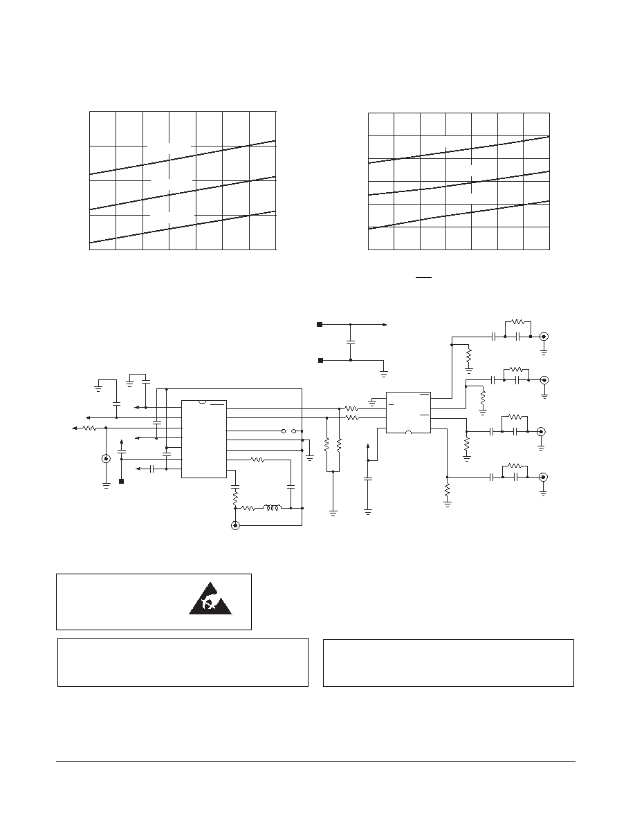
Fig. 5 Typical Application Circuit
Gennum Corporation assumes no responsibility for the use of any circuits described herein and makes no representations that they are free from patent infringement.
© Copyright July 2004 Gennum Corporation. All rights reserved. Printed in Canada.
DOCUMENT IDENTIFICATION:
DATA SHEET
The product is in production. Gennum reserves the right to
make changes at any time to improve reliability, function or
design, in order to provide the best product possible.
REVISION NOTES:
New document.
For latest product information, visit www.gennum.com
GENNUM CORPORATION
MAILING ADDRESS:
P.O. Box 489, Stn. A, Burlington, Ontario, Canada L7R 3Y3
Tel. +1 (905) 632-2996 Fax +1 (905) 632-2814
SHIPPING ADDRESS:
970 Fraser Drive, Burlington, Ontario, Canada L7L 5P5
GENNUM JAPAN CORPORATION
Shinjuku Green Tower Building 27F 6-14-1, Nishi Shinjuku Shinjuku-ku,
Tokyo 160-0023 Japan
Tel: +81 (03) 3349-5501 Fax: +81 (03) 3349-5505
GENNUM UK LIMITED
25 Long Garden Walk Farnham, Surrey, England GU9 7HX
Tel: +44 (0) 1252 747000 Fax: +44 (0) 1252 726523
CAUTION
ELECTROSTATIC
SENSITIVE DEVICES
DO NOT OPEN PACKAGES OR HANDLE
EXCEPT AT A STATIC-FREE WORKSTATION
L1
18n
R9
75
4
3
2
1
5
6
7
8
R13
150
C13
1.0
R8
68
C18
1.8p
C16
1.8p
R15
1.0
R7
100
R10
100
R11
680
R12
680
C14
100n
R14
68
R6
150
C11
1.8p
C10
1.0
R5
68
R3
150
V
CC
V
CC
V
CC
V
CC
V
CC
V
CC
V
CC
C6
1.0
R2
68
C8
1.8p
R15
150
J3
SDO4
J4
SDO4
J5
SDO4
J6
SDO4
GS9007
C3
100n
R1
50
1
2
3
4
5
6
7
14
13
12
11
10
9
8
J1
SDI
J2
OEM
C15
47p
C12
47p
GS9004D
JP1 OEM
113
TP1
SSI
C4 100n
C2
100n
10µ
+
C7
100n
C5
10µ
+
100n
V
CC
V
CC
OEM
V
CC
N/C
SSI
AGC
DATA
DATA
GND1
GND
GND
IN -
IN+
GND
+5V
SO2
SO2
SO1
SO1
GND
SI
SI
VCC
75