
∑ automatic cable equalization (typically 300m of high
quality cable at 270Mb/s)
∑ fully compatible with SMPTE 259M and operational
to 400 Mb/s
∑ adjustment free receiver when used with the
GS9000B or GS9000S decoder and GS9010A
Automatic Tuning Sub-system
∑ signal strength indicator
∑ selectable cable or direct digital inputs
∑ 28 pin PLCC packaging
APPLICATIONS
∑ 4
SC
, 4:2:2 and 360 Mb/s serial digital interfaces
GENLINX
TM
GS9005A
Serial Digital Receiver
DATA SHEET
FEATURES
DEVICE DESCRIPTION
The GS9005A is a monolithic IC designed to receive SMPTE
259M serial digital video signals. This device performs the
functions of automatic cable equalization and data and clock
recovery. It interfaces directly with the
GENLINX
TM
GS9000B
or GS9000S decoder, and GS9010A Automatic Tuning
Subsystem.
The VCO centre frequencies are controlled by external resistors
which can be selected by applying a two bit binary code to the
Standards Select input pins.
An additional feature is the Signal Strength Indicator output
which provides a 0.5V to 0V analog output relative to V
CC
indicating the amount of equalization being applied to the
signal.
The GS9005A is packaged in a 28 pin PLCC operating from a
single +5 or -5 volt supply.
Revision Date: August 1997
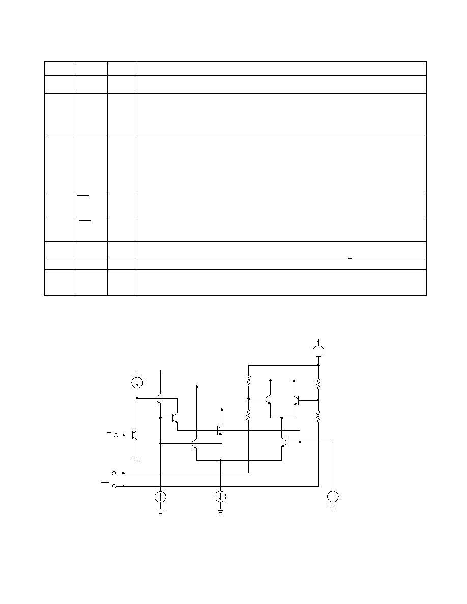
FUNCTIONAL BLOCK DIAGRAM
ORDERING INFORMATION
PART NUMBER
PACKAGE TEMPERATURE
GS9005ACPJ
28 Pin PLCC
0
O
C to 70
O
C
GS9005ACTJ
28 Pin PLCC Tape
0
O
C to 70
O
C
SERIAL DATA
PLL
SERIAL CLOCK
LOOP
FILTER
SS0
SS1
EQUALIZER
CARRIER
DETECT
CABLE
IN
DIGITAL
IN
SIGNAL
STRENGTH
INDICATOR
AGC
CAPACITOR
LOGIC
COMPARATOR
FILTER
CONTROL
VOLTAGE
VARIABLE
FILTER
DC
RESTORER
DATA
LATCH
PHASE
COMPARATOR
CARRIER
DETECT
CHARGE
PUMP
STANDARD
SELECT
PEAK
DETECTOR
VCO
ANALOG
DIGITAL
SELECT
28
8,9
5,6
19
12
13 14 15 17
20
21
2
1
A/D
SERIAL DATA
SERIAL CLOCK
24
25
22
23
16
OUTPUT 'EYE'
MONITOR
˜
2
/2 ENABLE
10
GS9005A
SPECIAL NOTE: R
VCO1
and R
VCO2
are functional over a
reduced temperature range of T
A
=0
∞
C to 50
∞
C. R
VCO0
and R
VCO3
are functional over the full temperature range
of T
A
=0
∞
C to 70
∞
C. This limitation does not affect
operation with the GS9010A ATS.
GENNUM CORPORATION P.O. Box 489, Stn A, Burlington, Ontario, Canada L7R 3Y3 tel. (905) 632-2996 fax: (905) 632-5946
Gennum Japan Corporation: A-302 Miyamae Village, 2-10-42 Miyamae, Suginami-ku, Tokyo 168, Japan tel. (03) 3334-7700 fax (03) 3247-8839
Document No. 520 - 28 - 11
2
520 - 28 - 11
PARAMETER SYMBOL
CONDITIONS
MIN
TYP
MAX UNITS NOTES
Supply Voltage
V
S
Operating Range
4.75
5.0
5.25
V
Power Consumption
P
D
-
500
700
mW
Supply Current (Total)
I
S
-
122
160
mA see Figure13
Serial Data & - High
V
OH
T
A
= 25
∞
C
-1.025
-
-0.88
V with respect to V
CC
Clock Output - Low
V
OL
T
A
= 25
∞
C
-1.9
-
-1.6
V
Logic Inputs - High
V
IH MIN
+2.0
-
-
V with respect to V
EE
- Low
V
IL MAX
-
-
+0.8
V with respect to V
EE
Carrier Detect
V
CDL
R
L
= 10 k
to V
CC
-
0.2
0.4
V
Output Voltage
V
CDH
4.0
5.0
-
V
Signal Strength
V
SS
See Note 2
-0.6
-
0
V with respect to V
CC
Indicator Output
Direct Digital Input
V
DDI
200
-
2000
mVp-p Differential Drive
Levels (5, 6)
Serial Data Bit Rate
BR
SDO
T
A
= 25
∞
C
100
-
400
Mb/s
Serial Clock Frequency
SLK
T
A
= 25
∞
C
100
-
400 MHz see Figure11
Output Signal Swing
V
O
T
A
= 25
∞
C
700
800
900
mV p-p see Figure12
Serial Data to Serial Clock
t
d
See Waveforms
-
-500
-
ps Data lags Clock
Lock Times
t
LOCK
See Note 1
-
-
10
µ
s
Equalizer Gain
AV
EQ
T
A
= 25
∞
C
30
36
-
dB at 135 MHz
Jitter
t
J
T
A
= 25
∞
C
-
±
100
-
ps p-p see Figure15
0 metres, 270 Mb/s
Input Resistance (SDI/SDI) R
IN
T
A
= 25∞C 3k
5k
-
see Figure14
Input Capacitance (SDI/SDI) C
IN
T
A
= 25∞C -
1.8
-
pF see Figure14
Output Eye Monitor
V
OEM
R
L
= 50
to V
CC
-
40
-
mVp-p
ABSOLUTE MAXIMUM RATINGS
PARAMETER
VALUE / UNITS
Supply Voltage
5.5 V
Input Voltage Range (any input)
V
CC
+0.5 to V
EE
-0.5 V
DC Input Current (any one input)
5 mA
Power Dissipation
750 mW
Operating Temperature Range
0
∞
C
T
A
70
∞
C
Storage Temperature Range
-65
∞
C
T
S
150
∞
C
Lead Temperature (soldering, 10 seconds)
260
∞
C
V
S
= 5V, T
A
= 0
∞
C to 70
∞
C, R
L
= 100
to (V
CC
- 2V) unless otherwise shown.
(1, 10, 20, 21)
GS9005A RECEIVER DC ELECTRICAL CHARACTERISTICS
with respect to V
CC
with respect to V
EE
Open
Collector - Active High
V
S
= 5V, T
A
= 0
∞
C to 70
∞
C, R
L
= 100
to (V
CC
- 2V) unless otherwise shown.
GS9005A RECEIVER AC ELECTRICAL CHARACTERISTICS
PARAMETER SYMBOL CONDITION MIN TYP MAX UNITS NOTES
Synchronization
NOTES: 1.
Switching between two sources of the same data rate.
2.
With weaker signals V
SS
approaches V
CC
.
CAUTION
ELECTROSTATIC
SENSITIVE DEVICES
DO NOT OPEN PACKAGES OR HANDLE
EXCEPT AT A STATIC-FREE WORKSTATION
3
520 - 28 - 11
The GS9005A Reclocking Receiver is a bipolar integrated
circuit containing a built-in cable equalizer and circuitry
necessary to re-clock and regenerate the NRZI serial data
stream.
Packaged in a 28 pin PLCC, the receiver operates from a
single five volt supply at data rates in excess of 400 Mb/s.
Typical power consumption is 500 mW. Typical output jitter is
±
100 ps at 270 Mb/s.
Serial Digital signals are applied to either a built-in analog
cable equalizer via the SDI and SDI inputs (pins 8,9) or via the
direct digital inputs DDI and DDI (pins 5,6).
Cable Equalizer
The Serial Digital signal is connected to the input either
differentially or single ended with the unused input being
decoupled. The equalized signal is generated by passing the
cable signal through a voltage variable filter having a
characteristic which closely matches the inverse cable loss
characteristic. Additionally, the variation of the filter
characteristic with control voltage is designed to imitate the
variation of the inverse cable loss characteristic as the cable
length is varied.
The amplitude of the equalized signal is monitored by a peak
detector circuit which produces an output current with a
polarity corresponding to the difference between the desired
peak signal level and the actual peak signal level. This output
is integrated by an external AGC filter capacitor (AGC
CAP pin 2), providing a steady control voltage for the voltage
variable filter.
A separate signal strength indicator output, (SSI pin 28),
proportional to the amount of AGC is also provided. As the
filter characteristic is varied automatically by the application of
negative feedback, the amplitude of the equalized signal is
kept at a constant level which is representative of the original
amplitude at the transmitter.
The equalized signal is then DC restored, effectively restoring
the logic threshold of the equalized signal to its correct level
irrespective of shifts due to AC coupling.
As the final stage of signal conditioning, a comparator converts
the analog output of the DC restorer to a regenerated digital
output signal.
An OUTPUT 'EYE' MONITOR (pin 16), allows verification of
signal integrity after equalization but before reslicing.
Analog/Digital Select
A 2:1 multiplexer selects either the equalized (analog) signal
or a differential ECL data (digital) signal as input to the
reclocker PLL.
A logical HIGH applied to the Analog/Digital Select input (1)
routes the equalized signal while a logic LOW routes the
direct digital signal to the reclocker.
Phase Locked Loop
The phase comparator itself compares the position of
transitions in the incoming signal with the phase of the local
oscillator (VCO). The error-correcting output signals are fed
to the charge pump in the form of short pulses. The charge
pump converts these pulses into a "charge packet" which is
accurately proportional to the system phase error.
The charge packet is then integrated by the second-order
loop filter to produce a control voltage for the VCO.
During periods when there are no transitions in the signal, the
loop filter voltage is required to hold precisely at its last value
so that the VCO does not drift significantly between corrections.
Commutating diodes in the charge pump keep the output
leakage current extremely low, minimizing VCO frequency
drift.
The VCO is implemented using a current-controlled
multivibrator, designed to deliver good stability, low phase
noise and wide operating frequency capability. The frequency
range is design-limited to
±
10% about the oscillator centre
frequency.
VCO Centre Frequency Selection
The centre frequency of theVCO is set by one of four external
current reference resistors (RVCO0-RVCO3) connected to
pins 13,14,15 or 17. These are selected by two logic inputs
SS0 and SS1 (pins 20, 21) through a 2:4 decoder according
to the following truth table.
SS1
SS0 Resistor Selected
0
0
RVCO0 (13)
0
1
RVCO1 (14)
1
0
RVCO2 (15)
1
1
RVCO3 (17)
As an alternative, the GS9010A Automatic Tuning Sub-system
and the GS9000B or GS9000S Decoder may be used in
conjunction with the GS9005A to obtain adjustment free and
automatic standard select operation (see Figure 20).
With the VCO operating at twice the clock frequency, a clock
phase which is centred on the eye of the locked signal is used
to latch the incoming data, thus maximising immunity to
jitter-induced errors. The alternate phase is used to latch the
output re-clocked data SDO and SDO (pins 25, 24). The true
and inverse clock signals themselves are available from the
SCO and SCO pins 23 and 22.
GS9005A Re - clocking Receiver - Detailed Device Description

4
520 - 28 - 11
SD0
SD0
SC0
SC0
SS1
SS0
CD
DDI
DDI
V
CC2
SDI
SDI
V
CC1
V
EE1
CAP A/D SS
I
V
EE2
V
CC4
GS9005A
TOP VIEW
LOOP R
VCO0
R
VCO1
R
VCO2
OEM R
VCO3
V
CC3
FILT
25
24
23
22
21
20
19
5
6
7
8
9
10
11
12 13 14 15 16 17 18
4 3 2 28 27 26
AGC
/2 EN
V
EE3
GS9005 & GS9005A PIN DESCRIPTIONS
PIN NO. SYMBOL
TYPE
DESCRIPTION
1
A/D
Input
Analog/Digital Select.
TTL compatible input used to select the input signal source. A logic HIGH routes the
Equalizer inputs (pins 8 and 9) to the PLL and a logic LOW routes the Direct Digital inputs (pins 5 and 6)
to the PLL.
2
AGC CAP
Input
AGC Capacitor.
Connection for the AGC capacitor.
3
V
EE1
Power Supply.
Most negative power supply connection. (Equalizer)
4
V
CC1
Power Supply
. Most positive power supply connection. (Equalizer)
5,6
DDI/DDI
Input
Direct Data Inputs (true and inverse).
Pseudo-ECL, differential serial data inputs. These are selected
when the A/D input (pin 1) is at logic LOW and are self biased to 1.2 volts below V
CC
. They may be
directly driven from true ECL drivers when V
EE
= -5V and V
CC
= 0 V.
7
V
CC2
Power Supply
. Most positive power supply connection. ( Phase detector, A/D select, carrier detect).
8,9
SDI/SDI
Input
Serial Data Inputs (true and inverse).
Differential analog serial data inputs. Inputs must be AC
coupled and may be driven single ended. These inputs are selected when the A/D input (pin 1) is
logic HIGH.
10 /2 EN
Input
/2 Enable-
TTL compatible input used to enable the divide by 2 function.
11 V
EE3
Power Supply.
Most negative power supply connection. (VCO, Mux, Standard Select)
12
LOOP FILT
Loop Filter.
Node for connecting the loop filter components.
13
R
VCO0
Input
VCO Resistor 0.
Analog current input used to set the centre frequency of the VCO when the two
Standard Select bits (pins 20 and 21) are set to logic 0,0. A resistor is connected from this pin to V
EE
.
14
R
VCO1
Input
VCO Resistor 1.
Analog current input used to set the centre frequency of the VCO when Standard
Select bit 0 (pin 20) is set HIGH and bit 1 (pin 21) is set LOW. A resistor is connected from this pin to V
EE
.
15
R
VCO2
Input
VCO Resistor 2.
Analog current input used to set the centre frequency of the VCO when Standard
Select bit 0 (pin 20) is set LOW and bit 1 (pin 21) is set HIGH. A resistor is connected from this pin to V
EE
.
16 OEM
Output
Output Eye Monitor
Analog voltage representing the serial bit stream after equalization but before reslicing.
17 R
VCO3
Input
VCO Resistor 3.
Analog current input used to set the centre frequency of the VCO when the two
Standard Select bits (pins 20 and 21) are set HIGH. A resistor is connected from this pin to V
EE
.
Fig. 2 GS9005A Pin Connections
tD
SERIAL
DATA OUT
(SD0)
50%
SERIAL
CLOCK OUT
(SCK)
tD
50%
Fig.1 Waveforms
5
520 - 28 - 11
PIN NO SYMBOL TYPE
DESCRIPTION
18 V
CC3
Power Supply.
Most positive power supply connection. (VCO, MUX, standards select).
19
CD
Output
Carrier Detect
. Open collector output which goes HIGH when a signal is present at either the Serial
Data inputs or the Direct Digital inputs. This output is used in conjunction with the GS9000B or GS9000S
in the Automatic Standards Select Mode to disable the 2 bit standard select counter. This pin should
see a low impedance (e.g. 1nF to AC Gnd)
20,21
SS0, SS1 Inputs
Standard Select Inputs.
TTL inputs to the 2:4 multiplexer used to select one of four VCO
centre
frequency setting resistors (R
VCO0
- R
VCO3
). When both SS0 and SS1 are LOW, R
VCO0
is selected.
When SS0 is HIGH and SS1 is LOW, R
VCO1
is selected. When SS0 is LOW and SS1 is HIGH, R
VCO2
is selected and when both SS0 and SS1 are HIGH, R
VCO3
is selected. These pins should see a
low impedance (e.g. 1nF to AC Gnd)
22,23 SCO/SCO Outputs
Serial Clock Outputs (inverse and true).
Pseudo-ECL differential outputs of the extracted serial clock.
These outputs require 390
pull-down resistors to V
EE
.
24,25
SDO/SDO Outputs
Serial Data Outputs (inverse and true).
Pseudo-ECL differential outputs of the regenerated serial data.
These outputs require 390
pull-down resistors to V
EE
.
26
V
CC4
Power Supply.
Most positive power supply connection. (ECL outputs)
27
V
EE2
Power Supply.
Most negative power supply connection. (Phase detector, A/D select, Carrier detect)
28
SS
I
Signal Strength Indicator.
Analog output which indicates the amount of AGC action. This output
indirectly indicates the amount of equalization and thus cable length.
GS9005 & GS9005A PIN DESCRIPTIONS cont.
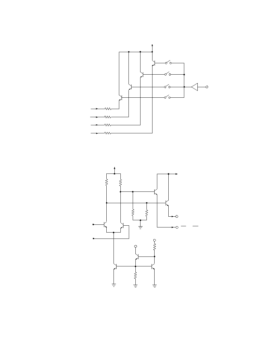
Fig. 3 Pins 1, 5 and 6
V
CC
V
CC
+
-
+
-
16µA
VCC
2k
2k
1k
1k
1.6V
380µA
50µA
A / D
DDI
Pin 1
Pin 5
Pin 6
DDI
V
CC
1.2V
INPUT / OUTPUT CIRCUITS
6
520 - 28 - 11
V
CC4
SDO or SCO
Pin 25, 24
10k
200
SDO or SCO
Pin 23, 22
V
CC
V
CC
V
CC
200
800
10k
3k
I
VCO
400
Pin 15
Pin 17
RVCO 0
Pin 13
Pin 14
400
400
400
RVCO 1
RVCO 2
RVCO 3
LOOP FILTER
(1.8 - 2.7V)
(1.9 - 2.4V)
INPUT / OUTPUT CIRCUITS cont.
Fig. 4 Pins 13, 14, 15 and 17
Fig. 5 Pins 25, 24, 23 and 22

7
520 - 28 - 11
V
CC
V
CC
+
-
920
µ
A
920
µ
A
AGC CAP
620
5k
5k
5k
500
0.4V
SSI
Pin 8
Pin 9
Pin 2
Pin 28
SDI
SDI
2V
+
-
INPUT / OUTPUT CIRCUITS cont.
Pin 12
LOOP FILTER
V
CC
V
CC
1k
V
CC
2k
1.5k
Fig. 7 Pin 12
10k
V
CC
Pin 19
CD
Fig. 9 Pin 19
Fig. 6 Pins 28, 2, 8 and 9
V
CC
Pin 20
SSO
V
CC
40µA
40µA
Pin 21
SS1
V
CC
Pin 10
/2 EN
V
CC
V
CC
+
-
18µA
55µA
480µA
1.6V
Fig. 10 Pins 20, 21 and 10
200
V
CC
Pin 16
5mA
OEM
5mA
Fig. 8 Pin 16

8
520 - 28 - 11
-j0.2
-j0.5
-j1
-j2
Frequencies in MHz, impedances normalized to 50
.
Fig. 14 Equalizer Input Impedance
j1
0 0.2 0.5 1 2 5
-j5
j5
j2
j0.5
j0.2
3000
1620
810
270
SERIAL OUTPUTS (mV)
TYPICAL PERFORMANCE CURVES
(V
S
= 5V, T
A
= 25
∞
C)
FREQUENCY (MHz)
500
450
400
350
300
250
200
150
100
50
1
2 3 4 5 6 7 8 9 10
FREQUENCY SETTING RESISTANCE (k
)
Fig. 11 Clock Frequency
CURRENT (mA)
140
135
130
125
120
115
110
105
100
0 10 20 30 40 50 60 70
TEMPERATURE (
∞
C)
Fig. 13 Supply Current
V
S
= 4.75V
V
S
= 5.00V
V
S
= 5.25V
900
850
800
750
700
650
600
0 10 20 30 40 50 60 70
TEMPERATURE (
∞
C)
Fig. 12 Serial Outputs
/2 OFF
/2 ON
V
S
= 5.00V
V
S
= 5.25V
V
S
= 4.75V
JITTER p-p (ps)
INPUT CABLE LENGTH - 8281 (m)
Fig. 15 Output Jitter vs Input Cable Length
at 143 & 270 Mb/s
0 25 50 75 100 125 150 175 200 225 250 275 300
800
700
600
500
400
300
200
100
0
270 Mb/s
143 Mb/s

9
520 - 28 - 11
TEST SETUP
Figure 16 shows a typical circuit for the GS9005A using a +5
volt supply. The four 0.1
µ
F decoupling capacitors must be
placed as close as possible to the corresponding V
CC
pins.
The loop voltage can be conveniently measured across the
10nF capacitor in the loop filter. Tuning procedures are
described in the Temperature Compensation Section
(page 11). The fixed value frequency setting resistors should
be placed close to the corresponding pins on the GS9005A.
The layout of the loop filter and RVCO components requires
careful attention. This has been detailed in an application
note entitled "Optimizing Circuit and Layout Design of the
GS9005A/15A", Document No. 521 - 32 - 00.
When the Direct Digital Inputs are not used, one of these
inputs should be connected to V
CC
to avoid picking up noise
and unwanted signals.
The Carrier Detect is an open-collector active high output
requiring a pull-up resistor of approximately 10 k
.
The SS0, SS1, CD pins should see a low AC impedance. This
is particularly important when driving the SS0, SS1 pins with
external logic. The use of 1 nF decoupling capacitors at these
pins ensures this.
Figure 17 shows the GS9005A connections when using a -5
volt supply.
Fig.16 GS9005A Typical Test Circuit Using +5V Supply
+
ECL
DATA
INPUTS
0.1
µ
100
100
100
100
390
390
DATA
DATA
CLOCK
CLOCK
390
390
0.1
µ
10
µ
0.1
µ
25
24
23
22
21
20
19
5
6
7
8
9
10
11
4 3 2 1 28 27 26
12 13 14 15 16 17 18
910
22n
75
113
75
47p
5.6p
10n
+5V
˜
1
˜
2
0.1
µ
47p
0.1
µ
10k
CARRIER
DETECT
OUTPUT
See Figure 18
+5V
+5V
+5V
+5V
INPUT
GS9005A
DD
I
DD
I
VCC2
SD
I
SD
I
/2
VEE3
SDO
SDO
SCO
SCO
SS1
SS0
CD
VCC1
VEE1
AGC
A/D
SS
I
VEE2
VCC4
LOOP
RVCO0
RVCO1
RVCO2
EYEOUT
RVCO3
VCC3
SSI
STAR
ROUTED
LOOP
VOLTAGE
TEST
POINT
ANALOG
+5V
DIGITAL
All resistors in ohms, all capacitors in microfarads, all inductors in henries unless otherwise stated.

10
520 - 28 - 11
VCO Frequency Setting Resistors
There are two modes of VCO operation available in the
GS9005A. When the /2 ENABLE (pin 10) is LOW, any of the
four VCO frequency setting resistors, RVCO0
through RVCO3
(pins 13, 14, 15 and 17) may be used for any data rate from 100
Mb/s to over 400 Mb/s. For example, for 143 Mb/s data
rate, the value of the total R
VCO
resistance is approximately
6k8 and for 270 Mb/s operation, the value is approximately
3k5. The 5k potentiometers will then tune the desired data rate
near their mid-points.
Jitter performance at the lower data rates (143, 177 Mb/s) is
improved by operating the VCO at twice the normal frequency.
This is accomplished by enabling the /2 function which
activates an additional divide by two block in the PLL section
of the GS9005A.
When the /2 ENABLE is HIGH two of the RVCO pins are
assigned to data rates below 200 Mb/s and two are assigned
to data rates over 200 Mb/s.
The selection is dependent upon the level of the STANDARD
SELECT BIT, SS1 (pin 21). When SS1 is LOW, RVCO0
and
RVCO1 (pins 13 and 14) are used for the higher data rates.
When SS1 is HIGH, the VCO frequency is now twice the bit rate
and its frequency is set by RVCO2 and RVCO3 (pins 15 and
17).
For 143 Mb/s and 270 Mb/s operation, (the VCO is at 286 MHz
and 270 MHz respectively) the total resistance required is
approximately the same for both data rates. This also applies
for 177 Mb/s and 360 Mb/s operation (the VCO is tuned to
354 MHz and 360 MHz respectively). This means that one
potentiometer may be used for each frequency pair with only
a small variation of the fixed resistor value. This halves the
number of adjustments required.
Fig. 17 GS9005A Typical Test Circuit Using -5V Supply
10
µ
ECL
DATA
INPUTS
0.1
µ
DATA
DATA
CLOCK
100
100
100
100
390
390
390
390
0.1
µ
+
0.1
µ
25
24
23
22
21
20
19
5
6
7
8
9
10
11
4 3 2 1 28 27 26
12 13 14 15 16 17 18
910
22n
75
113
75
47p
-5V
-5V
-5V
˜
1
˜
2
0.1
µ
47p
0.1
µ
-5V
10k
CARRIER
DETECT
OUTPUT
INPUT
GS9005A
DD
I
DD
I
VCC2
SD
I
SD
I
/2
VEE3
SDO
SDO
SCO
SCO
SS1
SS0
CD
VCC1
VEE1
AGC
A/D
SS
I
VEE2
VCC4
LOOP
RVCO0
RVCO1
RVCO2
EYEOUT
RVCO3
VCC3
SSI
LOOP
VOLTAGE
See Figure 18
ANALOG
DIGITAL
5.6p
-5V
-5V
-5V
-5V
-5V
10n
STAR
ROUTED
CLOCK
All resistors in ohms, all capacitors in microfarads, all inductors in henries unless otherwise stated.

11
520 - 28 - 11
5.6k
V
EE
1N914
1.3k
1.3k
5k
Divide by 2 is OFF
4.3k
V
EE
1N914
5k
Divide by 2 is ON
V
EE
1k
1k
Divide by 2 is OFF
Divide by 2 is ON
V
EE
1N914
1k
1k
0.1µF
0.1µF
0.1µF
0.1µF
1N914
Figure 18 shows the connections for the frequency setting
resistors for the various data rates. The compensation shown
for 360 Mb/s and 177 Mb/s with Divide by 2 ON, is useful to
a maximum ambient temperature of 50
∞
C. If the Divide by 2
function is not enabled by the /2 ENABLE input, no compen-
sation is needed for the 143 Mb/s and 177 Mb/s data rates.
The resistor connections are shown in Figure 19. In both
cases, the 0.1
µ
F capacitor that bypasses the potentiometer
should be star routed to VEE 3.
Temperature Compensation
Loop Bandwidth
The loop bandwidth is dependant upon the internal PLL gain
constants along with the loop filter components connected to
pin 12. In addition, the impedance seen by the RVCO pin also
influences the loop characteristics such that as the imped-
ance drops, the loop gain increases.
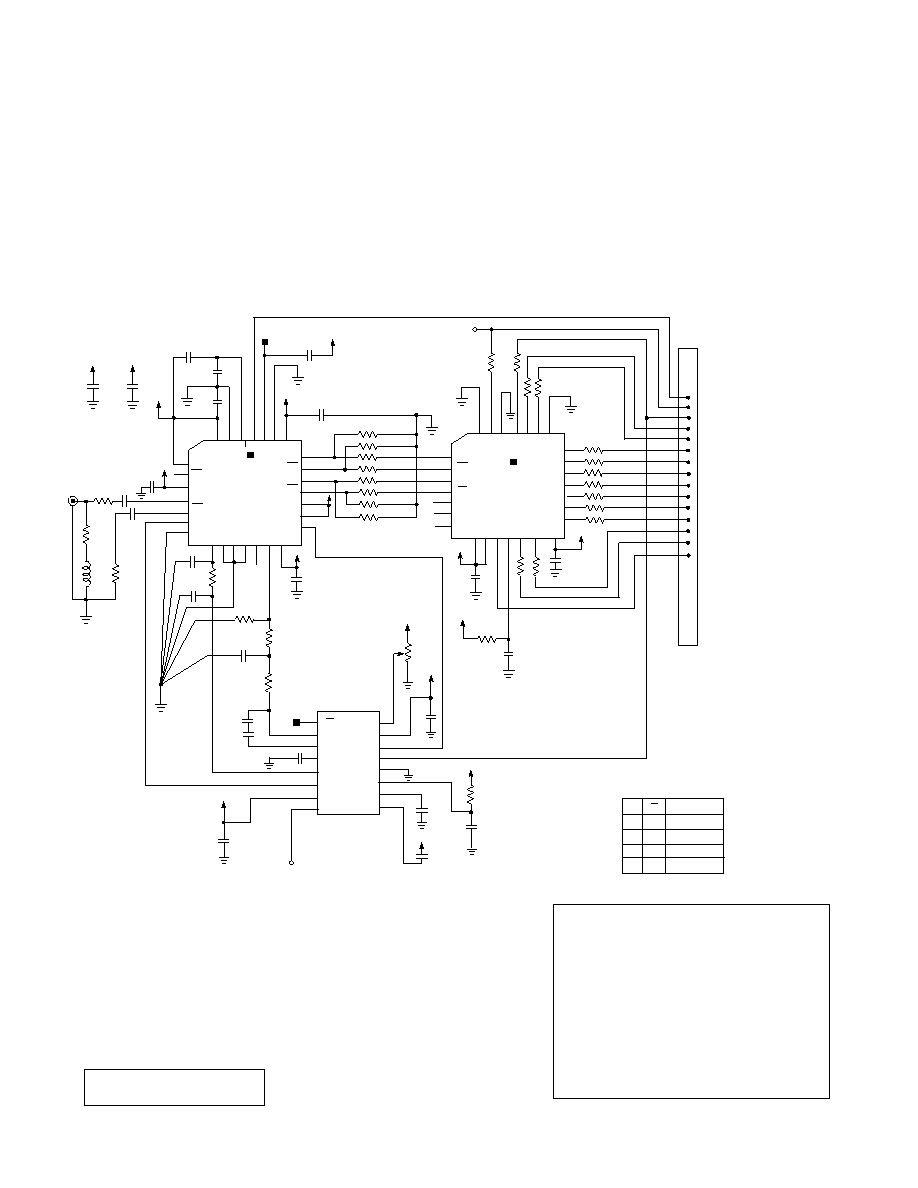
Applications Circuit
Figure 20 shows an application of the GS9005A in an
adjustment free, multi-standard serial to parallel convertor.
This circuit uses the GS9010A Automatic Tuning Sub-
system IC and a GS9000B or GS9000S Decoder IC. The
GS9005A may be replaced with a GS9015A Reclocker IC
if cable equalization is not required.
The GS9010A ATS eliminates the need to manually set or
externally temperature compensate the Receiver or Reclocker
VCO. The GS9010A can also determine whether the incoming
data stream is 4sc NTSC,4sc PAL or component 4:2:2.
The GS9010A includes a ramp generator/oscillator which
repeatedly sweeps the Receiver VCO frequency over a set
range until the system is correctly locked. An automatic
fine tuning (AFT) loop maintains the VCO control voltage at
it's centre point through continuous, long term adjustments
of the VCO centre frequency.
When an interruption to the incoming data stream is detected
by the Receiver, the Carrier Detect goes LOW and opens
the AFT loop in order to maintain the correct VCO frequency
for a period of at least 2 seconds. This allows the Receiver
to rapidly relock when the signal is re-established.
During normal operation, the GS9000B or GS9000S Decoder
provides continuous HSYNC pulses which disable the
ramp/oscillator of the GS9010A. This maintains the
correct Receiver VCO frequency.
Divide by 2 is OFF
V
EE
1k
0.1µF
10k
143Mb/s and 177 Mb/s using any R
VCO0
pins
Fig. 19 Non - Temperature Compensated Resistor Values
for 143 Mb/s and 177 Mb/s
Temperature Compensation Procedure
In order to correctly set the VCO frequency so that the PLL will
always re-acquire lock over the full temperature range, the
following procedure should be used. The circuit should be
powered on for at least one minute prior to starting this
procedure.
Monitor the loop filter voltage at the junction of the loop filter
resistor and 10 nF loop filter capacitor (LOOP FILTER TEST
POINT). Using the appropriate network shown above, the
VCO frequency is set by first tuning the potentiometer so that
the PLL loses lock at the low end (lowest loop filter voltage).
The loop filter voltage is then slowly increased by adjusting the
the potentiometer to determine the error free low limit of the
capture range. Error free operation is determined by using a
suitable CRC or EDH measurement method to obtain a stable
signal with no errors. Record the loop filter voltage at this point
as V
CL
. Now adjust the potentiometer so that the loop filter
voltage is 250 mV above V
CL
.
Fig. 18 Frequency Setting Resistor Values
& Temperature Compensation
270 Mb/s using R
VCO0
or R
VCO1
143 Mb/s using R
VCO2
or R
VCO3
177 Mb/s using R
VCO2
or R
VCO3
360 Mb/s using R
VCO0
or R
VCO1
12
520 - 28 - 11
STANDARD TRUTH TABLE
/2 P/N STANDARD
0 0 4:2:2 - 270
0 1 4:2:2 - 360
1 0 4sc - NTSC
1 1 4sc - PAL
P/N
OUT
IN-
COMP
LF
/2
VCC
SWF
1
2
3
4
5
6
7
8
16
15
14
13
12
11
10
9
PARALLEL DATA BIT 9
PARALLEL DATA BIT 8
PARALLEL DATA BIT 7
PARALLEL DATA BIT 6
PARALLEL DATA BIT 5
PARALLEL DATA BIT 4
PARALLEL DATA BIT 3
PARALLEL DATA BIT 2
PARALLEL DATA BIT 1
PARALLEL DATA BIT 0
PARALLEL CLOCK OUT
SYNC CORRECTION ENABLE
HSYNC OUTPUT
SYNC WARNING FLAG
INPUT SELECTION
STDT
VCC
CD
HSYNC
GND
OSC
DLY
FVCAP
10
µ
10
µ
10
µ
+
+
+
V
CC
+5V
+5V
V
CC
V
CC
V
CC
0.1
µ
100
100
100
100
390
390
390
390
0.1
µ
0.1
µ
0.1
µ
25
24
23
22
21
20
19
5
6
7
8
9
10
11
4 3 2 1 28 27 26
12 13 14 15 16 17 18
910
22n
(1)
(2)
(2)
(2)
(3)
75
113
75
47p
5.6p
10n
0.1
µ
0.1
µ
3.3n
82n
180n
SWF
0.68
µ
0.1
µ
0.1
µ
F
22n
DGND
DGND
DGND
DGND
47p
0.1
µ
DGND
GND
1.2k
1.2k
68k
100
100
120
50k
0.1
µ
100k
SWF
GS9010A
INPUT
ECL
DATA
INPUT
DD
I
DD
I
VCC2
SD
I
SD
I
/2
VEE3
SDO
SDO
SCO
SCO
SS1
SS0
CD
VCC1
VEE1
AGC
A/D
SS
I
VEE2
VCC4
LOOP
RVCO0
RVCO1
RVCO2
EYEOUT
RVCO3
VCC3
25
24
23
22
21
20
19
5
6
7
8
9
10
11
4 3 2 1 28 27 26
0.1
µ
DGND
DGND
SSI
100
100
100
3.3k
100
100
100
100
100
100
100
GS9000B
or GS9000S
SD
I
SD
I
SC
I
SC
I
SS1
SS0
SST
PD7
PD6
PD5
PD4
PD3
PD2
PD1
VSS
SWF
VSS
HSYNC
PD9
PD8
VSS
VDD
VDD
SCE
SWC
PCLK
PDO
VDD
STAR
ROUTED
12 13 14 15 16 17 18
V
CC
V
CC
V
CC
V
CC
6.8
µ
6.8
µ
+
+
GS9005A
V
CC
V
CC
DV
CC
DV
CC
DV
CC
V
CC
DV
CC
V
CC
(4)
Gennum Corporation assumes no responsibility for the use of any circuits described herein and makes no representations that they are free from patent infringement.
© Copyright March 1991 Gennum Corporation. All rights reserved. Printed in Canada.
REVISION NOTES
Changes to Figures 16, 17 and 20.
All resistors in ohms, all capacitor
in microfarads, all inductors in
henries unless otherwise stated.
Fig. 20 Typical Application Circuit
Application Note - PCB Layout
Special attention must be paid to component layout when designing high performance serial digital receivers. For background
information on high speed circuit and layout design concepts, refer to Document No. 521-32-00, "Optimizing Circuit and Layout
Design of the GS90005A/15A". A recommended PCB layout can be found in the Gennum Application Note "EB9010B
Deserializer Evaluation Board."
The use of a star grounding technique is required for the loop filter components of the GS9005A/15A.
Controlled impedance PCB traces should be used for the differential clock and data interconnection between the GS9005A and
the GS9000B or GS9000S. These differential traces must not pass over any ground plane discontinuities. A slot antenna is formed
when a microstrip trace runs across a break in the ground plane.
The series resistors at the parallel data output of the GS9000B or GS9000S are used to slow down the fast rise/fall time of the
GS9000B or GS9000S outputs. These resistors should be placed as close as possible to the GS9000B or GS9000S output pins
to minimize radiation from these pins.
DOCUMENT IDENTIFICATION
PRODUCT PROPOSAL
This data has been compiled for market investigation purposes
only, and does not constitute an offer for sale.
ADVANCE INFORMATION NOTE
This product is in development phase and specifications are
subject to change without notice. Gennum reserves the right to
remove the product at any time. Listing the product does not
constitute an offer for sale.
PRELIMINARY
The product is in a preproduction phase and specifications are
subject to change without notice.
DATA SHEET
The product is in production. Gennum reserves the right to
make changes at any time to improve reliability, function or
design, in order to provide the best product possible.
(1) Typical value for input return loss matching
(2) To reduce board space, the two anti-series 6.8
µ
F capacitors (connected across pins 2 and 3
of the GS9010A) may be replaced with a 1.0
µ
F non-polarized capacitor provided that:
(a) the 0.68
µ
F capacitor connected to the OSC pin (11) of the GS9010A is replaced with a
0.33
µ
F capacitor and
(b) the GS9005A /15A Loop Filter Capacitor is 10nF.
(3) Remove this potentiometer if P/N function is not required, and ground pin 16 of the GS9010A.
(4) The GS9000B will operate to a maximum frequency of 370 Mbps. The GS9000S will operate to
a maximum frequency of 300 Mbps.