 | –≠–ª–µ–∫—Ç—Ä–æ–Ω–Ω—ã–π –∫–æ–º–ø–æ–Ω–µ–Ω—Ç: GS9008 | –°–∫–∞—á–∞—Ç—å:  PDF PDF  ZIP ZIP |
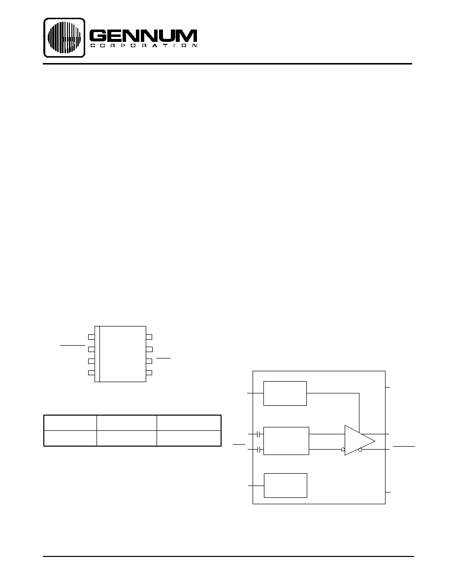
ORDERING INFORMATION
Part Number Package Type Temperature Range
GS9008 - CKA 8 Pin SOIC 0
∞
to 70
∞
C
DEVICE DESCRIPTION
The
GENLINX
TM
GS9008 is a bipolar integrated circuit
designed to drive two 75
co-axial cables at data rates
exceeding 400 Mb/s. It directly interfaces with other
GENLINX
TM
devices and can also be used as a general
purpose high speed cable driver.
While there are no plans to discontinue the GS9008, Gennum
has developed a successor product with improved features
and performance called the GS9028. The GS9028 is
recommended for new designs.
The differential inputs are AC-coupled and internally DC-
restored which allows correct passage of pathological
check codes associated with the serial digital standards.
Even though the inputs are AC coupled, static protection
diodes at each input restrict the DC differential so that if the
driving source uses the opposite polarity power supply,
external DC blocking capacitors must be used.
Correctly terminated output signal levels are adjustable
from as low as 0 mV to as high as 1100 mV with little change
in other performance parameters. Performance is guaranteed
for output levels between 600 mV and 1000 mV. The gain
of the output stages is varied by adjusting the V
SET
voltage
with respect to an internal band gap reference voltage
V
REF
.
The GS9008 is packaged in an 8 pin SOIC, and operates
from a single +5 or -5 volt supply consuming typically only
170 mW of power.
GENLINX
TM
GS9008 Cable Driver
with Two Adjustable Outputs
DATA SHEET
Revision Date: April 1998
FUNCTIONAL BLOCK DIAGRAM
OUTPUT 1
OUTPUT 1
GS9008
INPUT
V
SET
INPUT BUFFER
&
DC RESTORE
V
REF
INPUT
GAIN
CONTROL
V
CC
(GND)
GND (V
EE
)
BAND-GAP
REFERENCE
OUTPUT
DRIVER
FEATURES
∑ two outputs, adjustable from 0 to 1100 mVp-p into
75
loads
∑ nominal 600 ps rise and fall times
∑ accepts SMPTE and standard ECL input levels
∑ operates from a single +5 or -5 volt supply
∑ on-chip DC restoration for low jitter
∑ 170 mW power dissipation
∑ interfaces with
GENLINX
TM
GS9002, GS9004A,
GS9005A and GS9015A
APPLICATIONS
∑ SMPTE 259M Serial Digital Systems (4:2:2 & 4sc)
∑ Other Serial Digital Video Interfaces - 360 Mb/s
∑ General purpose high speed driver applications
INPUT
VSET
VEE
VREF
VCC
OUTPUT 1
OUTPUT 1
INPUT
8
1
4
3
6
5
7
2
GS9008
PIN CONNECTIONS
Patent No. 5,426,389.
Document No. 520 - 77 - 04
GENNUM CORPORATION P.O. Box 489, Stn. A, Burlington, Ontario, Canada L7R 3Y3 tel. +1 (905) 632-2996 fax. +1 (905) 632-5946
Web Site: www.gennum.com E-mail: info@gennum.com

2
520 - 77 - 3
Conditions: V
S
= 5V, T
A
= 0
∞
C to 70
∞
C, R
L
= 150
to GND and 144
AC coupled unless otherwise shown
Supply Voltage
V
S
4.5
5.0
5.5
volts
Power Consumption
P
D
2 x150
Loads DC
-
170
190
mW
Supply Current
I
S1
1% Accuracy, T
A
= 25
o
C
-
62
67
mA
V
SET
= (0.667) V
REF
Supply Current
I
S2
DC No Loads, T
A
= 25
o
C
-
16
20
mA
Reference Voltage
V
REF
10 k
to ground
-
1.2
-
volts
PARAMETER SYMBOL
CONDITIONS
MIN
TYP MAX UNITS NOTES
ABSOLUTE MAXIMUM RATINGS
PARAMETER
VALUE
Supply Voltage (V
S
)
5.5 V
Input Voltage Range (any input)
V
S
-0.5 V
Power Dissipation
300 mW
Operating Temperature Range
0
∞
C
T
A
70
∞
C
Storage Temperature Range
-65
∞
C
T
S
150
∞
C
Lead Temperature (soldering, 10 sec)
260
∞
C
Conditions: V
S
= 5V, T
A
= 0
∞
C to 70
∞
C, R
L
= 150
to GND and 144
AC coupled unless otherwise shown
GS9008 CABLE DRIVER - DC ELECTRICAL CHARACTERISTICS
GS9008 CABLE DRIVER - AC ELECTRICAL CHARACTERISTICS
Output Amplitudes across
75
Load (See Note 1)
Output Amplitude
Temperature Coefficient
(See Note 2)
Output
Rise/Fall Times (20% to 80%)
NOTE 1.
V
OUT
is measured across a correctly terminated load, back matched to the device. The peak to peak voltage of the device
itself is 2 x V
OUT
.
2.
V
OUT
is proportional to V
SET
and V
SET
may be an external low impedance, high stability supply. In this case the amplitude
temperature coefficient will not be guaranteed.
PARAMETER
SYMBOL CONDITIONS MIN TYP MAX UNITS
Input Signal Amplitude
V
IN
700
800
1000
mVp-p
Input Signal Rise/Fall Times
t
R
,t
F
-
-
750
ps
V
SET
= (0.5) V
REF
540
600
660
mVp-p Notes 1 & 2
V
OUT
V
SET
= (0.667) V
REF
720
800
880
mVp-p Notes 1 & 2
V
SET
= (0.833) V
REF
900
1000
1100 mVp-p Notes 1 & 2
V
SET
= (0.5) V
REF
-
25
100
ppm/
o
C
T
C
V
SET
= (0.667) V
REF
-
-12
80
ppm/
o
C
V
SET
= (0.833) V
REF
-
-45
80
ppm/
o
C
V
SET
= (0.5) V
REF
400
630
800
ps
t
R
,t
F
V
SET
= (0.667) V
REF
400
575
800
ps
V
SET
= (0.833) V
REF
400
530
800
ps
Output Overshoot
t
R
= t
F
= 600 ps
-
0
-
% See Fig. 3
Jitter
t
J
at 270 Mb/s
-
-
±
25
ps
Propagation Delay
t
P
- 1 - ns
3
520 - 77 - 3
VCC
400
400
V
OUT
V
OUT
V
CC
V
CC
INPUT / OUTPUT CIRCUITS
Fig. 2 Output Circuit (Pins 1 and 2)
Fig. 1 Input Circuit (Pins 6 and 7)
V
CC
0.5p
SERIAL
INPUTS
400
V
CC
V
REF1
V
REF1
+ V
REF2
+5V
-5V
6
7
0.1µF
0.1µF
-2V
ECL
DRIVER
GS9008
All resistors in ohms, all capacitors in microfarads unless otherwise stated.
Fig. 4 Split Supply Interfacing
All resistors in ohms, all capacitors in microfarads unless otherwise stated.
Fig. 3 Typical Application Circuit
INPUT SIGNAL
10k
+5V
150
1.0
0.1
INPUT SIGNAL
1.0
OUTPUT -1
(75
)
OUTPUT -1
(75
)
OUTPUT LEVEL
ADJUST
1.8p
68
1.8p
68
8
1
4
3
6
5
7
2
+
10
0.1
150
GS9008
4
520 - 77 - 3
Gennum Corporation assumes no responsibility for the use of any circuits described herein and makes no representations that they are free from patent infringement.
© Copyright March 1993 Gennum Corporation. All rights reserved. Printed in Canada.
DOCUMENT IDENTIFICATION:
DATA SHEET
The product is in production. Gennum reserves the right to
make changes at any time to improve reliability, function or
design, in order to provide the best product possible.
REVISION NOTES:
New information added to Device Description
GENNUM CORPORATION
MAILING ADDRESS:
P.O. Box 489, Stn. A, Burlington, Ontario, Canada L7R 3Y3
Tel. +1 (905) 632-2996 Fax +1 (905) 632-2814
SHIPPING ADDRESS:
970 Fraser Drive, Burlington, Ontario, Canada L7L 5P5
GENNUM JAPAN CORPORATION
C-101, Miyamae Village, 2-10-42 Miyamae, Suginami-ku, Tokyo 168-0081, Japan
Tel. +81 (3) 3334-7700 Fax: +81 (3) 3247-8839
GENNUM UK LIMITED
Centaur House, Ancells Business Park, Ancells Road, Fleet, Hampshire, UK GU13 8UJ
Tel. +44 (1252) 761 039 Fax +44 (1252) 761 114
CAUTION
ELECTROSTATIC
SENSITIVE DEVICES
DO NOT OPEN PACKAGES OR HANDLE
EXCEPT AT A STATIC-FREE WORKSTATION