
GENNUM CORPORATION P.O. Box 489, Stn. A, Burlington, Ontario, Canada L7R 3Y3
Tel. +1 (905) 632-2996 Fax. +1 (905) 632-5946 E-mail: info@gennum.com
www.gennum.com
Revision Date: June 2004
Document No. 29782 - 1
DATA SHEET
GS9
009
A
NO
T RECOMMENDED FOR NEW DESIGNS
KEY FEATURES
∑ two output pairs, adjustable from 0 to 1100mVp-p into
75
loads
∑ nominal 600 ps rise and fall times
∑ accepts SMPTE and standard ECL input levels
∑ operates from a single +5 or -5 volt supply
∑ on-chip DC restoration for low jitter
∑ 250 mW power dissipation
∑ interfaces with GENLINXTM GS9002, GS9004A,
GS9005A and GS9015A
∑ Pb-free and Green
APPLICATIONS
∑
SMPTE 259M Serial Digital Systems (4:2:2 & 4sc)
∑
Other Serial Digital Video Interfaces -- 360Mb/s
∑
General purpose high speed driver applications
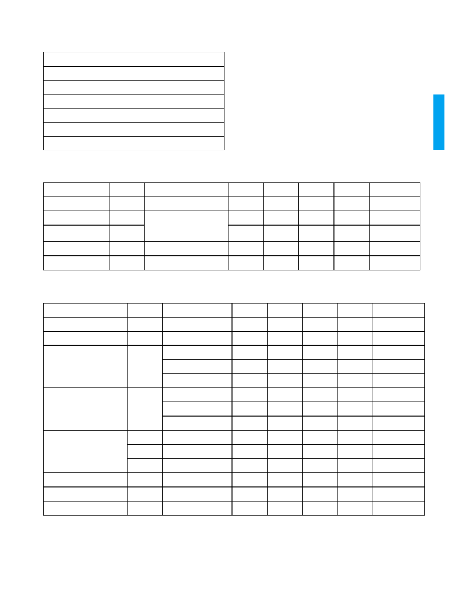
PIN CONNECTIONS
DESCRIPTION
The GENLINXTM GS9009A is a bipolar integrated circuit
designed to drive four 75
co-axial cables at data rates
exceeding 400Mb/s. It directly interfaces with other
GENLINXTM devices and can also be used as a general
purpose high speed cable driver.
The differential inputs are AC-coupled and internally DC-
restored which allows correct passage of pathological
check codes associated with the serial digital standards.
Even though the inputs are AC coupled, static protection
diodes at each input restrict the DC differential so that if the
driving source uses the opposite polarity power supply,
external DC blocking capacitors must be used.
Correctly terminated output signal levels are adjustable
from as low as 0mV to as high as 1100mV with little change
in other performance parameters. Performance is
guaranteed for output levels between 600 mV and 1000 mV.
The gain of the output stages is varied by adjusting the V
SET
voltage with respect to an internal bandgap reference
voltage V
REF
.
Pinout is compatible with the GS9007A by interchanging
pins 3,4,5,6,9,10,11,12 on the GS9009A with pins
1,2,3,4,5,6,7,8 on the GS9007A. In this way, a layout can be
made for either device depending on whether adjustability
is desired or not.
The GS9009A is packaged in a 14 pin SOIC, and operates
from a single +5 or -5 volt supply consuming typically only
250mW of power.
ORDERING INFORMATION
FUNCTIONAL BLOCK DIAGRAM
NC
NC
OUTPUT 1
OUTPUT 1
OUTPUT 2
NC
INPUT
OUTPUT 2
VSET
INPUT
VEE
VREF
NC
VCC
14
9
8
10
12
13
11
1
4
3
6
5
7
2
GS9009A
PART NUMBER
PACKAGE TYPE
TEMPERATURE RANGE
Pb-FREE AND GREEN
GS9009ACKB
14 Pin SOIC
0∞ to 70∞C
No
GS9009ACKBE3
14 Pin SOIC
0∞ to 70∞C
Yes
GS9009A
INPUT
V
SET
BAND-GAP
REFERENCE
INPUT BUFFER
&
DC RESTORE
V
REF
INPUT
GAIN
CONTROL
OUTPUT 1
V
CC
(GND)
OUTPUT 1
OUTPUT 2
OUTPUT 2
GND (V
EE
)
OUTPUT
DRIVER
OUTPUT
DRIVER
GENLINX
TM
GS9009A Cable Driver
with Four Adjustable Outputs
GENNUM CORPORATION
29782 - 1
2 of 4
GS9
009
A
NO
T RECOMMENDED FOR NEW DESIGNS
ABSOLUTE MAXIMUM RATINGS
GS9009A CABLE DRIVER -- DC ELECTRICAL CHARACTERISTICS
Conditions: V
S
= 5V, T
A
= 0∞C to 70∞C, R
L
= 150
to GND and 144 AC coupled unless otherwise shown
GS9009A CABLE DRIVER -- AC ELECTRICAL CHARACTERISTICS
Conditions: V
S
= 5V, T
A
= 0∞C to 70∞C, R
L
= 150
to GND and 144 AC coupled unless otherwise shown
PARAMETER
VALUE
Supply Voltage (V
S
)
5.5V
Input Voltage Range (any input)
V
S
-0.5V
Power Dissipation
300mW
Operating Temperature Range
0∞C
T
A
70∞C
Storage Temperature Range
-65∞C
T
S
150∞C
Lead Temperature (soldering, 10 sec)
260∞C
PARAMETER
SYMBOL
CONDITIONS
MIN
TYP
MAX
UNITS
NOTES
Supply Voltage
V
S
4.5
5.0
5.5
volts
Power Consumption
P
D
4 x150
Loads DC
1% Accuracy, T
A
= 25∞C
V
SET
= (0.667) V
REF
-
250
290
mW
Supply Current
S1
-
105
110
mA
Supply Current
S2
DC No Loads, T
A
= 25∞C
-
16
20
mA
Reference Voltage
V
REF
10 k
to ground
-
1.2
-
volts
PARAMETER
SYMBOL
CONDITIONS
MIN
TYP
MAX
UNITS
NOTES
Input Signal Amplitude
V
IN
700
800
1000
mVp-p
Input Signal Rise/Fall Times
tR,tF
-
-
750
ps
Output Amplitudes across
75
Load (See Note 1)
V
OUT
V
SET
= (0.5) V
REF
540
600
660
mVp-p
Note 1 & 2
V
SET
= (0.667) V
REF
720
800
880
mVp-p
Note 1 & 2
V
SET
= (0.833) V
REF
900
1000
1100
mVp-p
Note 1 & 2
Output Amplitude
Temperature Coefficient
(See Note 2)
T
C
V
SET
= (0.5) V
REF
-
25
100
ppm/∞C
V
SET
= (0.667) V
REF
-
-12
80
ppm/∞C
V
SET
= (0.833) V
REF
-
-45
80
ppm/∞C
Output
Rise/Fall Times (20% to
80%)
t
R
,t
F
V
SET
= (0.5) V
REF
400
630
800
ps
V
SET
= (0.667) V
REF
400
575
800
ps
V
SET
= (0.833) V
REF
400
530
800
ps
Output Overshoot
t
R
= t
F
= 600 ps
-
0
-
%
See Figure 3
Jitter
t
J
at 270Mb/s
-
-
±25
ps
Propagation Delay
t
P
-
1
-
ns
1. V
OUT
is measured across a correctly terminated load, back matched to the device. The peak to peak voltage of the device
itself is 2 x V
OUT
.
2. V
OUT
is proportional to V
SET
and V
SET
may be an external low impedance, high stability supply. In this case the amplitude
temperature coefficient will not be guaranteed.

GENNUM CORPORATION
29782 - 1
3 of 4
GS9
009
A
NO
T RECOMMENDED FOR NEW DESIGNS
INPUT/OUTPUT CIRCUITS
Figure 1 Input Circuit (Pins 11 and 12)
Figure 2 Output Circuit (Pins 3, 4 and 5, 6)
All resistors in ohms, all capacitors in microfarads unless otherwise stated.
Resistors marked 1, 2, 3 and 4 are 150
each.
Figure 3 Typical Application Circuit
All resistors in ohms, all capacitors in microfarads unless otherwise stated.
Figure 4 Split Supply Interfacing
V
CC
0.5p
SERIAL
INPUTS
400
V
CC
V
REF1
V
REF1
+ V
REF2
VCC
400
400
V
OUT
V
OUT
V
CC
V
CC
INPUT SIGNAL
+
10
0.1
1.0
1 2 3 4
1.0
OUTPUT -2
(75
)
+5V
0.1
INPUT SIGNAL
1.0
1.0
OUTPUT -2
(75
)
OUTPUT -1
(75
)
OUTPUT -1
(75
)
1.8p
1.8p
1.8p
1.8p
68
68
68
68
10k
OUTPUT LEVEL
ADJUST
8
9
10
5
6
7
3
4
2
1
11
12
13
14
GS9009A
+5V
-5V
10
11
0.1µF
0.1µF
-2V
ECL
DRIVER
GS9009A
29782 - 1
4 of 4
GENNUM CORPORATION
MAILING ADDRESS:
P.O. Box 489, Stn. A, Burlington, Ontario, Canada L7R 3Y3
Tel. +1 (905) 632-2996 Fax. +1 (905) 632-5946
SHIPPING ADDRESS:
970 Fraser Drive, Burlington, Ontario, Canada L7L 5P5
GENNUM JAPAN CORPORATION
Shinjuku Green Tower Building 27F, 6-14-1, Nishi Shinjuku,
Shinjuku-ku, Tokyo, 160-0023 Japan
Tel. +81 (03) 3349-5501, Fax. +81 (03) 3349-5505
GENNUM UK LIMITED
25 Long Garden Walk, Farnham, Surrey, England GU9 7HX
Tel. +44 (0)1252 747 000 Fax +44 (0)1252 726 523
Gennum Corporation assumes no responsibility for the use of any circuits described herein and makes no representations that they are free from patent infringement.
© Copyright October 2003 Gennum Corporation. All rights reserved. Printed in Canada.
GS9
009
A
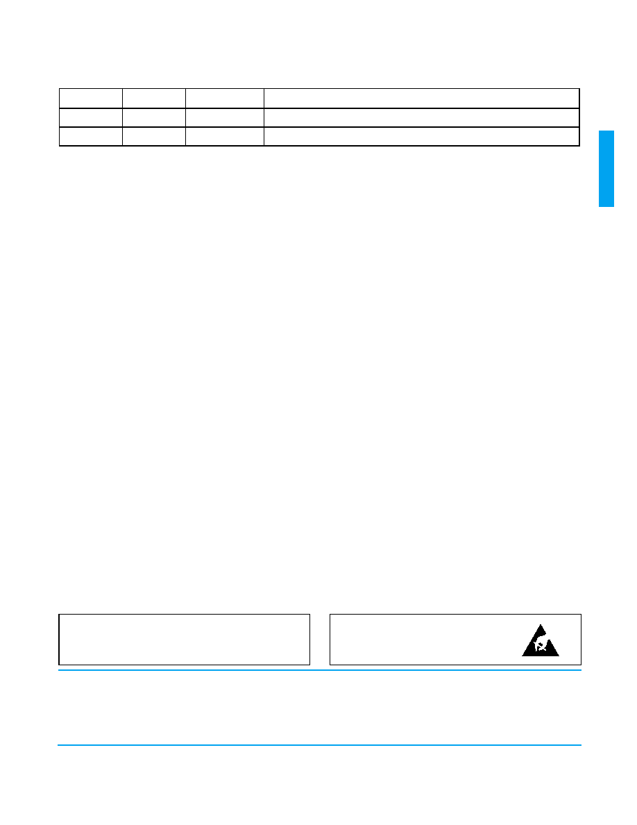
CAUTION
ELECTROSTATIC
SENSITIVE DEVICES
DO NOT OPEN PACKAGES OR HANDLE
EXCEPT AT A STATIC-FREE WORKSTATION
DOCUMENT IDENTIFICATION
PRELIMINARY DATA SHEET
The product is in a preproduction phase and specifications
are subject to change without notice.
NO
T RECOMMENDED FOR NEW DESIGNS
REVISION HISTORY
VERSION
ECR
DATE
CHANGES AND/OR MODIFICATIONS
0
132428
October 2003
New Document
1
134031
June 2004
Added lead-free and green information.