
GENNUM CORPORATION P.O. Box 489, Stn. A, Burlington, Ontario, Canada L7R 3Y3
Tel. +1 (905) 632-2996 Fax. +1 (905) 632-5946 E-mail: info@gennum.com
www.gennum.com
Revision Date: November 1999
Document No. 521 - 65 - 05
DATA SHEET
G
S
9
021
FEATURES
∑ Error Detection and Handling (EDH) according to
SMPTE RP-165
∑ EDH insertion and extraction in one device
∑ auto-standard operation with override via host
interface
∑ noise immune extraction of HVF timing signals
∑ TRS insertion/correction and ANC header correction
for all standards
∑ ITU-R-601 output clipping for active picture area
∑ selectable I≤C interface or 8-bit parallel port for access
to EDH flags and device configuration bits
∑ all error flags available on dedicated output pins
∑ 24-bit Errored Field counter
∑ BYPASS mode to bypass EDH insertion/updating
∑ dynamic blanking control input
∑ 8-bit or 10-bit compatibility
∑ up to 54MHz operating frequency
∑ seamless flag-mapping with GS9020 serial digital
video input processor
∑ 64 pin LQFP
APPLICATIONS
EDH processing for SMPTE 259M serial digital interfaces for
composite and component standards including 4:4:4:4 at
540Mb/s; Noise immune digital sync and timing generation.
Source, destination, distribution and test equipment;
General purpose, TRS formatted, blank video stream
generator with EDH.
DESCRIPTION
The GS9021 implements error detection and handling
(EDH) according to SMPTE RP-165. Interfacing to the
parallel inputs of either the GS9002, GS9022 or GS9032
serial digital encoders, the GS9021 is primarily used on the
transmit end of the SDI interface. The GS9021 provides
EDH insertion and extraction for 4sc NTSC, 4sc PAL and
all component PAL and NTSC standards including 4:2:2
(13.5MHz and 18MHz luminance sampling), and 4:4:4:4.
The GS9021 generates noise immune timing signals such
as horizontal sync, vertical blanking and field ID. In
addition, TRS-ID correction/insertion and data blanking are
implemented for all standards.
A host interface, configurable as an 8-bit parallel interface
or an I≤C (I≤C is a registered trademark of Philips) serial
interface allows for communication with a microcontroller.
The interface can be used to read and/or write the
complete set of error flags and override the flag status prior
to re-transmission. A 5-bit flag port provides access to all
error flags on dedicated pins for applications where the
microcontroller is not used. The device automatically
determines the operating standard, but this can be
overridden through the programming interface.
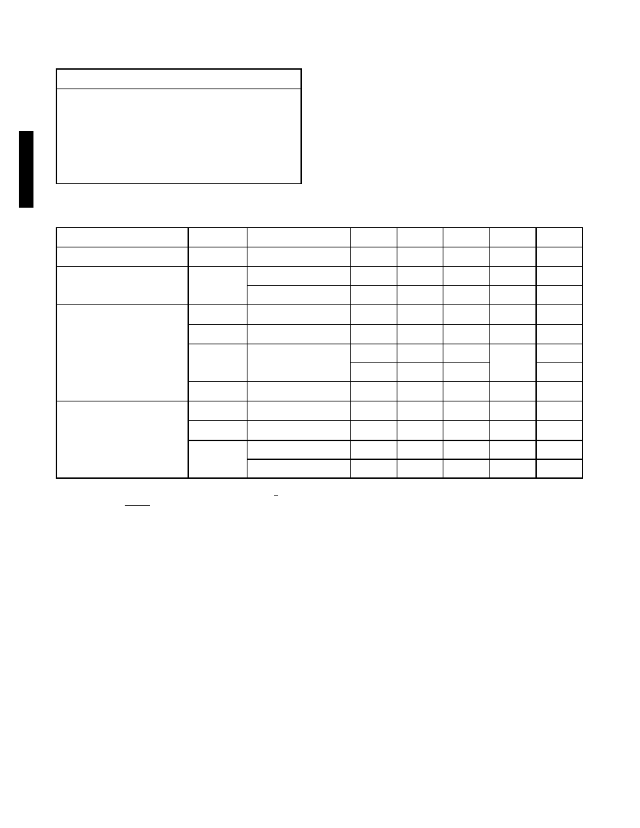
BLOCK DIAGRAM
ORDERING INFORMATION
PART NUMBER
PACKAGE
TEMPERATURE
GS9021-CFU
64 pin LQFP Tray
0∞C to 70∞C
GS9021-CTU
64 pin LQFP Tape
0∞C to 70∞C
DOUT
CRC_MODE
HOSTIF_MODE
8-BIT
PARALLEL
INTERFACE
BYPASS_EDH
DIN
VBLANKS/L
FLYWDIS
H, V, F
EDH FLAG
EXTRACTION
CRC
COMPARISON/
CALCULATION
ANCILLARY
CHECKSUM
CALCULATION/
COMPARISON
ANCILLARY
CHECKSUM
CORRECTION
10
LSB_TOP
HVF
FLYWHEEL
ERRORED
FIELD
COUNTER
TRS
DETECTION
DEDICATED
FLAG PORT
I≤C INTERFACE
FLAGS
DATA BUS
REVERSAL
MUX
ITU-R-601 CLIPPING
TRS BLANKING
TRS INSERTION/
CORRECTION
FLAG_MAP
NEW CRC
CALCULATION
TRS
COMPARE
TRS_ ERROR
CLIP_TRS
10
10
10
10
10
ERROR FLAGS
&
FORMAT PACKET
BLANK_EN
HOST INTERFACE/
FLAG PORT
5
R/T
I≤C is a registered
Trademark of Philips
GENLINX
TM
II
GS9021
EDH Coprocessor
521 - 65 - 05
2
G
S
902
1
ABSOLUTE MAXIMUM RATINGS
PARAMETER
VALUE
Supply Voltage
-0.3V to 6.0V
Input Voltage Range (any input)
-0.3 to V
DD
+ 0.3V
Operating Temperature Range
0∞C to 70∞C
Storage Temperature
-55∞C to 150∞C
Lead Temperature (soldering, 10 sec)
260∞C
DC ELECTRICAL CHARACTERISTICS
V
DD
= 5.0V, T
A
= 0 to 70∞C unless otherwise shown.
PARAMETER
SYMBOL
CONDITION
MIN
TYP
MAX
UNITS
NOTES
Supply Voltage
V
DD
4.75
5.0
5.25
V
Supply Current Unloaded
DD
27MHz
-
39
-
mA
54MHz
-
75
-
mA
TTL Compatible CMOS Inputs
V
ILMAX
-
-
0.8
V
V
IHMIN
2.0
-
-
V
IN
V
IN
= V
DD
or GND
-
-
150
µA
1
-
-
1
2
C
IN
-
10
-
pF
TTL Compatible CMOS Outputs
V
OLMAX
at
OUT
-
-
0.4
V
V
OHMIN
at
OUT
2.4
-
-
V
OUT
-
4
-
mA
3
-
2
-
mA
4
NOTES
1. The following inputs have internal pull-up resistors: R/T. The following inputs have internal pull-down resistors: FLYWIS, LSB_TOP,
CRC_MODE, RESET, FLAG_MAP, HOSTIF_MODE and DIN[9:0].
2. All other inputs.
3. The following outputs have 4mA drivers (typical): S[1:0], FL[4:0], DOUT[9:0], H, V and F[2:0].
4. The following outputs have 2mA drivers (typical): P[7:0].

521 - 65 - 05
3
G
S
9
021
AC ELECTRICAL CHARACTERISTICS
V
DD
= 5.0V, T
A
= 0 to 70∞C unless otherwise shown.
PARAMETER
SYMBOL
CONDITION
MIN
TYP
MAX
UNITS
NOTES
Input Clock Frequency
-
-
54
MHz
Clock Pulse Width Low
t
PWL
7.4
-
-
ns
Clock Pulse Width High
t
PWH
7.4
-
-
ns
Input Setup Time
t
S
3
-
-
ns
1, 2
Input Hold Time
t
H
3
-
-
ns
1, 2
Output Delay Time
t
OD
with 10pF loading
-
-
15
ns
2
Output Hold Time
t
OH
with 10pF loading
5
-
-
ns
2
Output Setup Time
t
OS
with 10pF loading
3.5
-
-
ns
2,4
Flag Port Disable Time
t
FDIS
with 25pF loading
-
-
15
ns
Flag Port Enable Time
t
FEN
with 25pF loading
-
-
16
ns
I≤C Clock Frequency
SCL
-
-
400
kHz
Host Interface Setup Time
t
HS
6
-
-
ns
Host Interface Hold Time
t
HH
6
-
-
ns
Host Interface Output
Enable Time
t
HEN
with 25pF loading
-
-
21
ns
Host Interface Output
Disable Time
t
HDIS
with 25pF loading
-
-
10
ns
Reset Time Pulse Width
t
RESET
100
-
-
ns
Device Latency
t
LAT
8
8
8
clks
3
NOTES
1. See section 1.2 for a list of signals synchronous and asynchronous to PCLKIN.
2. See Figures 1 and 2.
3. Latency is defined as the number of clock cycles between the time when the data is latched into the device and when the
corresponding output data is clocked into the next device as shown in Figure 3.
4) Based upon 54MHz clock (18.5ns). Output Setup Time = Clock Period - Output Delay Time

521 - 65 - 05
4
G
S
902
1
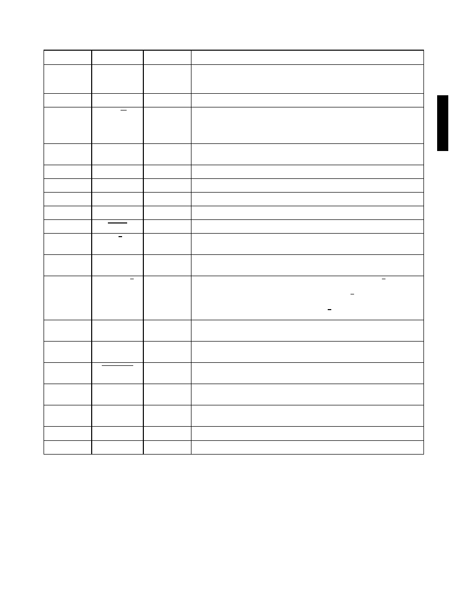
PIN CONNECTIONS
PIN DESCRIPTIONS
NUMBER
SYMBOL
TYPE
DESCRIPTION
1-7, 10-12
DIN[9:0]
I
Parallel digital video data inputs.
13
PCLKIN
I
Parallel clock input.
14-16
P[7:5]
I/O
In parallel port mode, these are bits 7:5 of the host interface address/data bus. In
I≤C mode, these pins must be set LOW.
17
SCL/P4
I/O
In parallel port mode, this is bit 4 of the host interface address/data bus. In I≤C
mode, this is the serial clock input for the I≤C port.
18
SDA/P3
I/O
In parallel port mode, this is bit 3 of the host interface address/data bus. In I≤C
mode, this is the serial data pin for the I≤C port.
19-21
A[2:0]/P[2:0]
I/O
In parallel port mode, these are bits 2:0 of the host interface address/data bus. In
I≤C mode, these are input bits which define the I≤C slave address for the device.
22
R/W
I
Parallel port read/write control. When HIGH, the parallel port is configured as an
output (read mode). When LOW, the parallel port is configured as an input (write
mode). In I≤C mode, this pin must be set HIGH.
23
A/D
I
Parallel port address/data bus control. When HIGH, the parallel port is used for
address input. When LOW, the parallel port is used for data input or output. In
I≤C mode, this pin must be set LOW.
24
CS
I
Parallel port chip select. When CS is LOW and R/W is HIGH, the GS9021 drives
the address/data bus. When CS is LOW and R/W is LOW, the user should drive
the address/data bus. When CS is HIGH, the address/data bus is in a high
impedance state (Hi - Z). In I≤C mode, this pin must be set HIGH.
25
HOSTIF_MODE
I
Host Interface mode select. When HIGH, the host interface is configured for I≤C
mode. When LOW, the host interface is configured for parallel port mode.
DIN9
DIN8
DIN7
DIN6
DIN5
DIN4
DIN3
V
DD
GND
DIN2
DIN1
DIN0
PCLKIN
P7
P6
P5
DOUT9
DOUT8
DOUT7
DOUT6
DOUT5
DOUT4
DOUT3
V
DD
GND
DOUT2
DOUT1
DOUT0
FLAG_MAP
F_R/W
FL4
FL3
CLIP_TRS
FLYWDIS
BLANK_EN
LSB_TOP
BYPASS_EDH
VBLANKS/L
CRC_MODE
V
DD
GND
R/T
RESET
F2
F1
F0
H
V
SCL/P4
SDA/P3
A2/P2
A1/P1
A0/P0
R/W
A/D
CS
HOSTIF_MODE
V
DD
GND
S0
S1
FL0
FL1
FL2
17 18 19 20 21 22 23 24 25 26 2728 29 30 31 32
64 63 62 61 60 59 58 57 56 55 54 53 52 51 50 49
1
2
3
4
5
6
7
8
9
10
11
12
13
14
15
16
GS9021
TOP VIEW
48
47
46
45
44
43
42
41
40
39
38
37
36
35
34
33
521 - 65 - 05
5
G
S
9
021
28, 29
S[1:0]
I/O
Control bits which select whether FF, AP, or ANC EDH flags are active on the EDH
flag data port (FL[4:0]). In FLAG_MAP mode, the S[1:0] pins become outputs
(see device description).
30-34
FL[4:0]
I/O
EDH flag data port to allow access to the EDH flags.
35
F_R/W
I
Flag port read/write control. When HIGH, FL[4:0] are configured as outputs
allowing EDH flags to be read from the device. When LOW, FL[4:0] are
configured as inputs allowing EDH flags to be overwritten into the outgoing EDH
packet. In FLAG_MAP mode this pin must be set HIGH.
36
FLAG_MAP
I
FLAG_MAP mode enable. When HIGH, FLAG_MAP mode is enabled. When
LOW, FLAG_MAP mode is disabled.
37-39, 42-48
DOUT[9:0]
O
Parallel digital video data outputs.
49
V
O
Vertical sync indication.
50
H
O
Horizontal sync indication.
51-53
F[2:0]
O
Field indication. F2 is the MSB.
54
RESET
I
Reset. When LOW, the internal control circuitry is reset.
55
R/T
I
Receive/Transmit mode select. When HIGH, the device operates in receive mode.
When LOW, the device operates in transmit mode.
58
CRC_MODE
I
CRC_MODE enable. When HIGH, CRC_MODE is enabled. When LOW,
CRC_MODE is disabled.
59
VBLANKS/L
I
Vertical blanking interval control. For NTSC signals, when VBLANKS/L is set LOW
the 19 line blanking interval is selected and when set HIGH the 9 line blanking
interval is selected. For PAL D2 signals, when VBLANKS/L is set LOW the 17 line
blanking interval is selected and when set HIGH the 7 line blanking interval is
selected. For PAL component signals VBLANKS/L should be set LOW.
60
BYPASS_EDH
I
Bypass EDH control. When HIGH, the device allows the EDH packet to pass
through unaltered.
61
LSB_TOP
I
Data output LSB position control. When HIGH, the video data output bus is
reversed, placing the LSB at pin 48.
62
BLANK_EN
I
Blanking enable. When LOW, incoming data words are set to appropriate
blanking levels.
63
FLYWDIS
I
Flywheel disable. When HIGH, the internal flywheel is disabled. When LOW, the
internal flywheel is enabled.
64
CLIP_TRS
I
Clip and TRS correction control. When HIGH, the TRS Blanking, ITU-R-601
clipping and TRS insertion features are enabled.
8, 26, 41, 57
V
DD
Power supply (nominally +5V).
9, 27, 40, 56
GND
Ground.
PIN DESCRIPTIONS
NUMBER
SYMBOL
TYPE
DESCRIPTION