GENLINX
TM
GS9022A
Digital Video Serializer
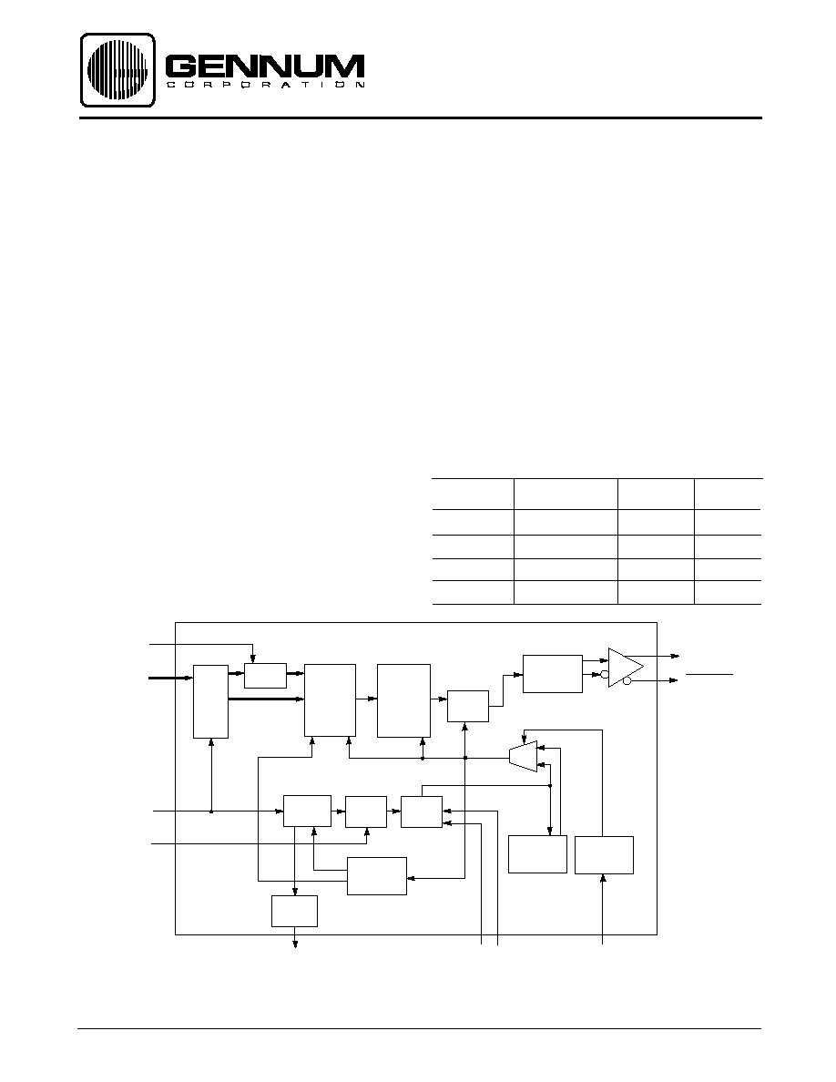
FUNCTIONAL BLOCK DIAGRAM
FEATURES
DEVICE DESCRIPTION
The GS9022A is a drop-in replacement for the GS9022 in
existing applications
The GS9022A is a monolithic bipolar integrated circuit designed
to serialize SMPTE 125M and SMPTE 244M bit parallel digital
signals as well as other 8 or 10 bit parallel formats. This device
performs the functions of sync detection, parallel to serial
conversion, data scrambling (using the X
9
+ X
4
+1 algorithm),
10x parallel clock multiplication and conversion of NRZ to
NRZI serial data. The data rate is automatically set for SMPTE
259M data rates to 400 Mb/s. Other features include a lock
detect output and an internal cable driver capable of driving
two 75
loads.
The device requires a single +5 volt or -5 volt supply and
typically consumes 650 mW of power while driving two 75
loads. The 28 pin PLCC packaging assures a small footprint
for the complete encoder function.
� built-in 75
W
cable driver with two serial outputs
� standard independent operation
� space saving 28 pin PLCC package
� 650 mW typical power dissipation (data output
driving 75
W
load).
� supports bit rates to 400 Mb/s
� accepts 8 bit and 10 bit TTL and CMOS
compatible parallel data inputs
� fully compatible with SMPTE 259M serial digital
standard
� single +5 or -5 volt supply
� Pb-free and Green
APPLICATIONS
� 4
SC
, 4:2:2 and 360 Mb/s serial digital interfaces for:
Video cameras
VTRs
Signal generators
Portable equipment
DATA SHEET
ORDERING INFORMATION
Revision Date: June 2004
Document No. 18325 - 01
GENNUM CORPORATION P.O. Box 489, Stn. A, Burlington, Ontario, Canada L7R 3Y3 tel. +1 (905) 632-2996 fax. +1 (905) 632-5946
Web Site: www.gennum.com E-mail: info@gennum.com
SYNC
DETECT
DISABLE
GS9022A
PLD
LOOP
FILTER
R
VCO
PCLK
PARALLEL
DATA
IN (10 BITS)
P/S
CONVERTER
SYNC
DETECT
REGULATOR CAP
PHASE
FREQUENCY
DETECT
CHARGE
PUMP
V
CO
INPUT
LATCH
DIV BY 10
GENERATOR
3-12
13
17
28
25
SCLK
LOCK
DETECT
SCRAMBLER
SERIAL DATA
SERIAL DATA
23
22
14
LOCK
DETECT
19
C
OSC
26
OSCILLATOR
DIV BY 2
GENERATOR
RISE TIME
CONTROL
NRZ
NRZI
MUX
NOT RECOMMENDED FOR NEW DESIGNS SEE GS9032
Part Number
Package
Temperature
Pb-Free
and Green
GS9022ACPJ
28 pin PLCC
o�C to 70�C
No
GS9022ACTJ
28 pin PLCC Tape
o�C to 70�C
No
GS9022ACPJE3
28 pin PLCC
o�C to 70�C
Yes
GS9022ACTJE3
28 pin PLCC Tape
o�C to 70�C
Yes

2 of 7
18325 - 01
NOT RECOMMENDED FOR NEW DESIGNS SEE GS9032
Serial Data Outputs
SDATA, SDATA
bit rates
BR
SDO
100
-
400
Mb/s
signal swing
V
SDO
R
L
= 75
720
800
880
mVp-p
rise/fall times
t
r
, t
f
(20 - 80%)
400
550
800
ps
jitter
t
j
270 Mb/s
240
-
ps p-p
Note 1
Lock Time
t
lock
C
Loop filt
= 0.1�F
-
5
-
ms
Auto Standard
R
Loop filt
= 3.9k
C
OSC
= 0.1�F
Parallel Data & Clock Inputs
risetime
t
R
TA = 25�C
500
-
-
ps
setup
t
SU
3
-
-
ns
hold
tHOLD
3
-
-
ns
PARAMETER SYMBOL CONDITIONS
MIN TYP MAX UNITS NOTES
Supply Voltage
V
S
Operating Range
4.75
5.0
5.25
V
Power Consumption
P
D
Data outputs driving two 75
loads
-
650
-
mW
T
A
= 25�C
Supply Current
I
S
Data outputs driving two 75
loads
-
160
190
mA
TTL Inputs-HIGH
V
IH
T
A
= 25�C
2.0
-
-
V
TTL Inputs-LOW
V
IL
T
A
= 25�C
-
-
0.8
V
Logic Input Current
I
IN
-
2.5
6.0
�A
TTL Outputs-HIGH
V
OH
T
A
= 25�C
2.4
-
-
V
TTL Outputs-LOW
V
OL
T
A
= 25�C
-
-
0.5
V
V
CC
= 5V, V
EE
= 0V, T
A
= 0�C
to 70�C unless otherwise shown
GS9022A - ENCODER DC ELECTRICAL CHARACTERISTICS
GS9022A - ENCODER AC ELECTRICAL CHARACTERISTICS
V
CC
= 5V, V
EE
= 0V, T
A
= 0�C
to 70�C, unless otherwise shown
PARAMETER
SYMBOL CONDITIONS MIN TYP MAX UNITS NOTES
ABSOLUTE MAXIMUM RATINGS
PARAMETER
VALUE/UNITS
Supply Voltage
5.5 V
Input Voltage Range (any input)
-V
EE
< V
I
< V
CC
DC Input Current (any one input)
10 mA
Power Dissipation (V
S
= 5.25 V)
910 mW
Operating Temperature Range
0
�
C
�
T
A
�
70
�
C
Storage Temperature Range
-65
�
C
�
T
S
�
150
�
C
Lead Temperature (soldering 10 seconds)
260
�
C
PIN CONNECTIONS
PD9 PCK LOCK V
EE
V
CC
LF
V
EE
IN DET
PD2
PD3
PD4
PD5
PD6
PD7
PD8
SYNC DET.
DISABLE
V
CCSD
SDO
SDO
V
EE
V
CC
R
VCO
PD1 PD0 V
CC
V
CC
C
REG
V
EE
C
OSC
GS9022A
TOP VIEW
25
24
23
22
21
20
19
5
6
7
8
9
10
11
12 13 14 15 16 17 18
4
3 2 28 27 26
CAUTION
ELECTROSTATIC
SENSITIVE DEVICES
DO NOT OPEN PACKAGES OR HANDLE
EXCEPT AT A STATIC-FREE WORKSTATION
Note 1:
Measured using PCLK as trigger source on 1 GHz oscilloscope
3 of 7
18325 - 01
NOT RECOMMENDED FOR NEW DESIGNS SEE GS9032
The charge pump delivers a 'charge packet' to the loop filter
which is proportional to the system phase error. Internal
voltage clamps are used to constrain the loop filter voltage
between approximately 1.8 and 3.4 volts.
The VCO, constructed from a current-controlled multivibrator,
features operation in excess of 400 Mb/s and a wide pull
range (
� 40% of centre frequency).
VCO Centre Frequency Selection
The wide VCO
pull range allows the PLL to compensate for
variations in device processing, temperature variations and
changes in power supply voltage, without external adjustment.
A single external resistor is used to set the VCO current for all
standards.
The COSC pin is used to configure the VCO of the GS9022A
in one of three modes, as shown below:
C
OSC
Mode
0.1�F to GND
Auto Standard
10k Resistor to VCC
/2 ON
10k Resistor to GND
/2 OFF
In auto standard mode, the capacitor sets the sweep rate at
which the VCO toggles between and /2.
The /2 ON and /2 OFF modes are used to configure the
GS9022A VCO for single standard operation.
The lock detect circuit disables the serial data output when the
loop is not locked. The Lock Detect output is available from pin
14 and is HIGH when the loop is locked.
The true and complement serial data, SDO and SDO are
available from pins 22 and 23. These outputs will drive
two 75
co-axial cables with SMPTE level serial digital
video signals.
Phase Locked Loop
The PLL performs parallel clock multiplication and provides
the timing signal for the serializer. It is composed of
a phase/frequency detector, charge pump, VCO
,
a
divide-by-ten counter, and a divide by two counter.
The phase/frequency detector allows a wider capture range
and faster lock time than that which can be achieved with a
phase discriminator alone. The discrimination of frequency
also eliminates harmonic locking. With this type of discriminator,
the PLL can be over-damped for good stability without
sacrificing lock time.
The GS9022A Serializer is a bipolar integrated circuit used to
convert parallel data into a serial format according to the
SMPTE 259M standard. The device encodes both eight and
ten bit TTL-compatible parallel signals producing serial data
rates up to 400 Mb/s. It operates from a single five volt supply
and is packaged in a 28 pin PLCC.
Functional blocks within the device include the input latches,
sync detector, parallel to serial converter, scrambler, NRZ to
NRZI
converter, internal cable driver, PLL for 10 x parallel
clock multiplication and lock detect.
The parallel data (PD0-PD9) and parallel clock (PCKIN) are
applied via pins 3 through 13 respectively.
Sync Detector
The Sync Detector looks for the reserved words 000-003 and
3FC-3FF, in ten bit hexadecimal, or 00 and FF in eight bit
hexadecimal, used in the TRS-ID sync word. When the
occurrence of either all zeros or all ones at inputs PD2-PD9 is
detected, the lower two bits PD0 and PD1 are forced to zeros
or ones, respectively. This makes the system compatible with
eight or ten bit data. For non - SMPTE standard parallel data,
a logic input, Sync Detect Disable (25) is available to disable
this feature.
Scrambler
The Scrambler is a linear feedback shift register used to
pseudo-randomize the incoming serial data according to the
fixed polynomial (X
9
+X
4
+1). This minimizes the DC component
in the output serial data stream. The NRZ to NRZI converter
uses another polynomial (X+1) to convert a long sequence of
ones to a series of transitions, minimizing polarity effects.
GS9022A Digital Video Serializer - Detailed Device Description

4 of 7
18325 - 01
NOT RECOMMENDED FOR NEW DESIGNS SEE GS9032
GS9022A PIN DESCRIPTIONS
PIN NO.
SYMBOL TYPE
DESCRIPTION
1
V
CC
Power Supply: Most positive power supply connection for the PLL and Scrambler.
2
V
CC
Power Supply: Most positive power supply connection for the parallel data inputs and P/S
converter.
3-12
PD0-PD9
I
TTL level inputs of the parallel data words. PD0 is the LSB and PD9 is the MSB.
13
PCKIN
I
TTL level input of the parallel clock.
14
LOCK DET
O
TTL level output which goes high when the internal PLL is locked.
15
V
EE
Power Supply: Most negative power supply connection.
16
V
CC
Power Supply: Most positive power supply connection for the PLL and Scrambler.
17
LF
I
Connection for the R-C loop filter components.
18
V
EE
Power Supply: Most negative power supply connection.
19
R
VCO
I
VCO frequency setting resistor. A 1% resistor is required.
20
V
CC
Power Supply: Most positive power supply connection for the PLL and Scrambler.
21
V
EE
Power Supply: Most negative power supply connection.
22, 23
SDO, SDO
I
75
cable driver outputs (true and inverse).
24
V
CCSD
Power Supply: Most positive power supply for cable driver outputs.
25
SYNC DET
TTL level input that disables the internal sync detector when high. This allows the GS9022 to
DISABLE
I
serialize 8 or 10 bit non-SMPTE standard parallel data.
26
C
OSC
I
Toggles VCO between and /2.
27
V
EE
I
Power Supply: Most negative power supply connection.
28
C
REG
I
Compensation capacitor for internal voltage regulator that requires decoupling with a
0.1 �F capacitor located as close as possible to the pin in series with an 820
Resistor.
5 of 7
18325 - 01
NOT RECOMMENDED FOR NEW DESIGNS SEE GS9032
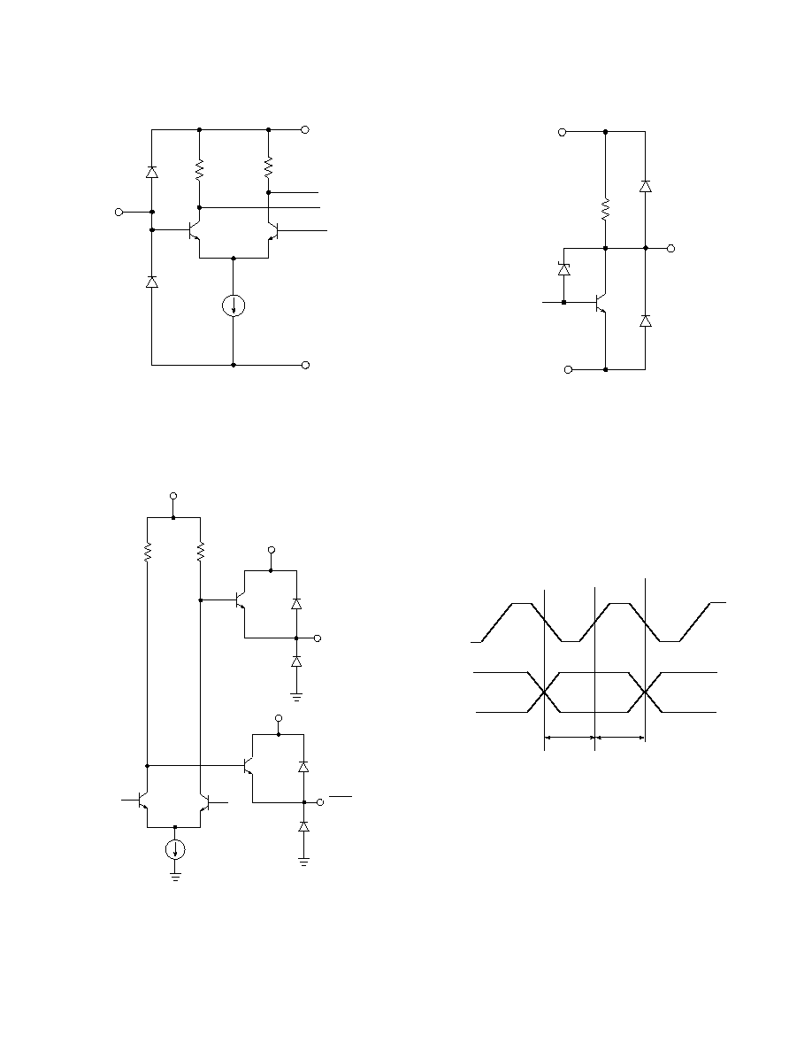
INPUT / OUTPUT CIRCUITS
Fig. 3 Output Circuit
Fig. 1 Sync Detect Disable, Parallel Data,
Parallel Clock
V
EE
1k
1k
V
CC
PINS 3-12
13, 25
V
R1
Fig. 2 Lock Detect
Fig. 4 Input Clock / Data Timing
LOCK
DETECT
10k
V
EE
V
CC
PIN 14
VCC
400
400
V
OUT
PIN 23
V
OUT
PIN 22
V
CC
V
CC
tSU
tHOLD
tCLKL = tCLKH
PARALLEL
CLOCK
PLCK
50%
PARALLEL
DATA
PDn