
GENNUM CORPORATION P.O. Box 489, Stn. A, Burlington, Ontario, Canada L7R 3Y3
Tel. +1 (905) 632-2996 Fax. +1 (905) 632-5946 E-mail: info@gennum.com
www.gennum.com
Revision Date: November 2000
Document No. 521 - 70 - 06
DATA SHEET
G
S
9
024
FEATURES
∑ automatic cable equalization
∑ fully compatible with SMPTE 259M
∑ typically equalizes greater than 350m of high quality
cable at 270Mb/s
∑ signal strength indicator
∑ output data muting when input data is lost
∑ output 'eye' monitor (OEM) with large signal amplitude
and power down option
∑ low power: 240mW at 5V
∑ 14 pin SOIC package
∑ programmable output data squelch for max cable
length limiting
∑ carrier detect with programmable threshold level
∑ serial data output "High Z" select to allow muxing of
EQ inputs
APPLICATIONS
Front-end cable equalization for digital video systems; Input
equalization for serial digital distribution amplifiers, routers,
production switchers and other receiving equipment.
DESCRIPTION
The GS9024 is a high performance automatic cable
equalizer designed for serial digital data rates from 143Mb/s
to 540Mb/s. The GS9024 receives either single-ended or
differential serial data and outputs equalized differential
signals at PECL levels (800mV). The GS9024 provides up to
40dB of gain at 200MHz which will typically result in
equalization of greater than 350m at 270Mb/s of Belden
8281 cable.
The GS9024 incorporates an analog signal strength
indicator/carrier detect (SSI/CD) output indicating both the
presence of a carrier and the amount of equalization
applied to the signal. Optional external resistors allow the
carrier detect threshold level to be customized to the user's
requirement.
The GS9024 also features selectable High Z serial data
outputs eliminating the need for input muxing circuitry in
routers. In addition, the GS9024 provides an 'Output Eye
Monitor' (OEM) which allows the verification of signal
integrity after equalization, prior to reslicing.
The GS9024 operates from a single +5V or -5V power
supply and consumes only 240mW of power. Packaged in a
small 14 pin SOIC, the GS9024 is ideal for router
applications where high density component placement is
required.
BLOCK DIAGRAM
ORDERING INFORMATION
PART NUMBER
PACKAGE
TEMPERATURE
GS9024-CKB
14 pin SOIC
0∞C to 70∞C
GS9024-CTB
14 pin SOIC Tape
0∞C to 70∞C
SDI
SDI
OEM
AGC CD_ADJ
+
-
+
-
+ -
+
-
HIGH Z
SDO
SDO
SSI/CD
VARIABLE GAIN
EQ STAGE
AUTO EQ
CONTROL
EYE
MONITOR
GENLINX
TM
II
GS9024
Automatic Cable Equalizer

GENNUM CORPORATION
521 - 70 - 06
2
G
S
9
024
ABSOLUTE MAXIMUM RATINGS
PARAMETER
VALUE
Supply Voltage
5.5V
Input Voltage Range (any input)
V
CC
+0.5 to V
EE
-0.5V
Operating Temperature Range
0∞C
T
A
70∞C
Storage Temperature Range
-65∞C
T
S
150∞C
Lead Temperature (soldering, 10 sec)
260∞C
DC ELECTRICAL CHARACTERISTICS
V
CC
= 5V, V
EE
= 0V, T
A
= 0∞C TO 70∞C unless otherwise shown.
PARAMETER
SYMBOL
CONDITIONS
MIN
TYP
1
MAX
UNITS
NOTES
TEST
LEVEL
Supply Voltage
V
CC
4.75
5.0
5.25
V
Power Consumption
P
D
-
240
-
mW
3
with OEM active
-
340
-
mW
3
Supply Current
S
-
44
-
mA
1
with OEM active
-
58
-
mA
1
Serial Data O/P Current
SDO
R
L
= 75
-
11
-
mA
3
SDI/SDI Common Mode
Voltage
-
2.5
-
V
1
AGC+/AGC- Mode
Voltage
-
2.7
-
V
1
OEM Bias Potential
-
4.5
-
V
1
SSI/CD Output Current
SOURCE
C
LM
AX
= 50pF R
L
=
-
-
18
µA
C
LM
AX
= 50pF R
L
= 5k
-
-
110
µA
SINK
-
1.0
1.5
mA
High Z Input Voltage
V
HIGH
2.4
-
-
V
1
V
LOW
-
-
0.8
V
1
TEST LEVELS
1. 100% tested at 25∞C.
2. Guaranteed by design.
3. Inferred or co-related value.
NOTES
1. Typical values are parametric norms at 25∞C.
GENNUM CORPORATION
521 - 70 - 06
3
G
S
9
024
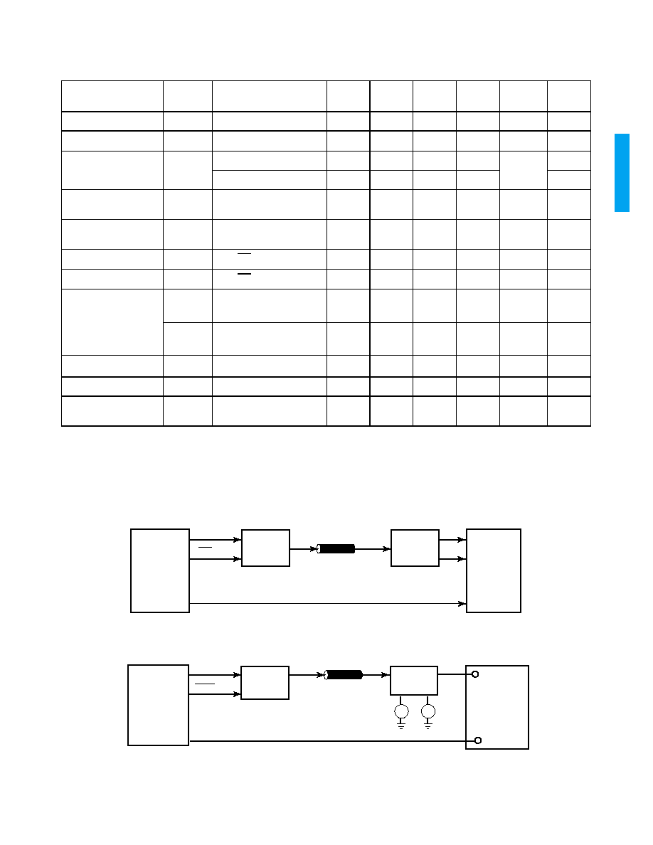
TEST SETUP
Fig. 1 Test Setup for Figure 3.
Fig. 2 Test Setup for Figures 4, 5, 6, 7, 10 and 11.
AC ELECTRICAL CHARACTERISTICS
V
CC
= 5V, V
EE
= 0V, T
A
= 0∞C TO 70∞C unless otherwise shown.
PARAMETER
SYMBOL
CONDITIONS
MIN
TYP
1
MAX
UNITS
NOTES
TEST
LEVEL
Data Rate
143
-
540
Mb/s
1
Output Signal Swing
V
SDO
R
L
= 75
700
850
1000
mV
1
Additive Jitter
t
J
270Mb/s, 300m
-
275
-
ps p-p
see
Fig 5
5
540Mb/s, 100m
-
200
-
ps p-p
5
Output Rise and Fall
Times (20-80%)
t
r
,
t
f
0.5
0.65
-
ns
3
Output Duty Cycle
Distortion
-
30
-
ps
2
Input Resistance
R
IN
SDI, SDI
-
10
-
k
2
Input Capacitance
C
IN
SDI, SDI
-
1.0
-
pF
2
Carrier Detect
Response Time
t
CDON
Carrier Applied R
L
=
,
C
L
50pF on SSI/CD
-
3
-
µs
2
t
CDOFF
Carrier Removed R
L
=
,
C
L
50pF on SSI/CD
-
30
-
µs
2
High Z Response Time
t
r
HIGHZ
-
17
-
ns
2
Input Return Loss
at 270MHz
15
20
-
dB
see Fig 8
3
Maximum Equalizer
Gain
A
EQ
at 200MHz
-
40
-
dB
see Fig 4
3, 5
TEST LEVELS
1. 100% tested at 25∞C.
2. Guaranteed by design.
3. Inferred or co-related value.
4. Evaluated using test setup Figure 1.
5. Evaluated using test setup Figure 2.
NOTES
1. Typical values are parametric norms at
25∞C.
EB9024
BOARD
GS9028
CABLE
DRIVER
TEKTRONIX
GigaBERT
700
ANALYZER
TEKTRONIX
GigaBERT
700
TRANSMITTER
BELDEN 8281
CABLE
DATA
DATA
CLOCK
TRIGGER
GS9028
CABLE
DRIVER
VERTICAL IN
TRIGGER IN
OSCILLOSCOPE
ANRITSU
ME522A
or
GigaBERT
700
TRANSMITTER
BELDEN 8281
CABLE
DATA
DATA
CLOCK
EB9024
BOARD
SSI/CD
CD_ADJ
V
V

GENNUM CORPORATION
521 - 70 - 06
4
G
S
9
024
PIN CONNECTIONS
PIN DESCRIPTIONS
NUMBER
SYMBOL
TYPE
DESCRIPTION
1, 14
AGC-, AGC+
I
External AGC capacitor.
4, 5
SDI/SDI
I
Differential serial digital data inputs.
8
OEM
O
Output `Eye' monitor. OEM is a single ended current mode output
and requires an external 50
pullup resistor.
9
CD_ADJ
I
Carrier detect threshold adjust.
10, 11
SDO/SDO
O
Equalized serial digital data outputs.
12
SSI/CD
O
Signal strength indicator/Carrier Detect.
13
HIGH Z
I
The SDO/SDO outputs are High Z when this pin is HIGH. If High Z
functionality is not used, this input can be left floating or tied LOW.
AGC-
V
EE
V
CC
SDI
SDI
HIGH Z
SDO
V
EE
V
CC
SDO
CD_ADJ
OEM
AGC+
SSI/CD
GS9024
TOP VIEW
1
2
3
4
5
6
7
14
13
12
11
10
9
8

GENNUM CORPORATION
521 - 70 - 06
5
G
S
9
024
TYPICAL PERFORMANCE CURVES (V
S
= 5V, T
A
= 25∞C unless otherwise shown.)
Fig. 3 Maximum Data Rate vs. Cable Length - Belden 8281n
(see Test Setup in Figure 1)
Fig. 4 Equalizer Gain vs. Frequency
Fig. 5 Additive Jitter vs. Input Cable Length - Belden 8281
Fig. 6 SSI/CD Voltage vs. Cable Length - Belden 8281
(CD_ADJ = 0V)
Fig. 7 Carrier Detect Adjust Voltage Threshold Characteristics
Fig. 8 Input Impedance
DATA RATE (Mb/s)
CABLE LENGTH (m)
500
400
300
200
100
0
90 180 270 360 450 540 630
0.5 UI
Output
Additive
Jitter
0.2 UI
Output
Additive
Jitter
0
5
10
15
20
25
30
35
40
45
50
1
10
100
1000
GAIN (dB)
FREQUENCY (MHz)
0
200
400
600
800
1000
1200
1400
1500
0
50
100
150
200
250
300
350
ADDITIVE JITTER (ps p-p)
CABLE LENGTH (m)
540Mb/s
270Mb/s
5.00
4.50
4.00
3.50
3.00
2.50
0 50 100 150 200 250 300 350 400 450 500
SSI/CD OUTPUT VOLTAGE (V)
CABLE LENGTH (m)
200
250
300
350
400
CD_ADJ VOLTAGE (V)
CABLE LENGTH (m)
2.0
3.0
3.5
4.0
4.5
5.0
2.5
3000
1620
810
720
-j1
-j2
-j5
j2
j5
j1
j0.5
j0.2
-j0.2
-j0.5
Frequencies in MHz, impedances normalized to 50
.