GENNUM CORPORATION P.O. Box 489, Stn. A, Burlington, Ontario, Canada L7R 3Y3
Tel. +1 (905) 632-2996 Fax. +1 (905) 632-5946 E-mail: info@gennum.com
www.gennum.com
Revision Date: June 2000
Document No. 522 - 75 - 00
PRELIMINARY DATA SHEET
G
S
9
025
A
FEATURES
∑ SMPTE 259M compliant
∑ operational to 540Mb/s
∑ automatic cable equalization (typically greater than
350m of high quality cable at 270Mb/s)
∑ adjustment-free operation
∑ auto-rate selection (5 rates) with manual override
∑ single external VCO resistor for operation with five
input data rates
∑ data rate indication output
∑ serial data outputs muted and serial clock remains
active when input data is lost
∑ operation independent of SAV/EAV sync signals
∑ signal strength indicator output
∑ carrier detect with programmable threshold level
∑ power savings mode (output serial clock disable)
APPLICATIONS
Cable equalization plus clock and data recovery for all high
speed serial digital interface applications involving SMPTE
259M and other data standards.
DESCRIPTION
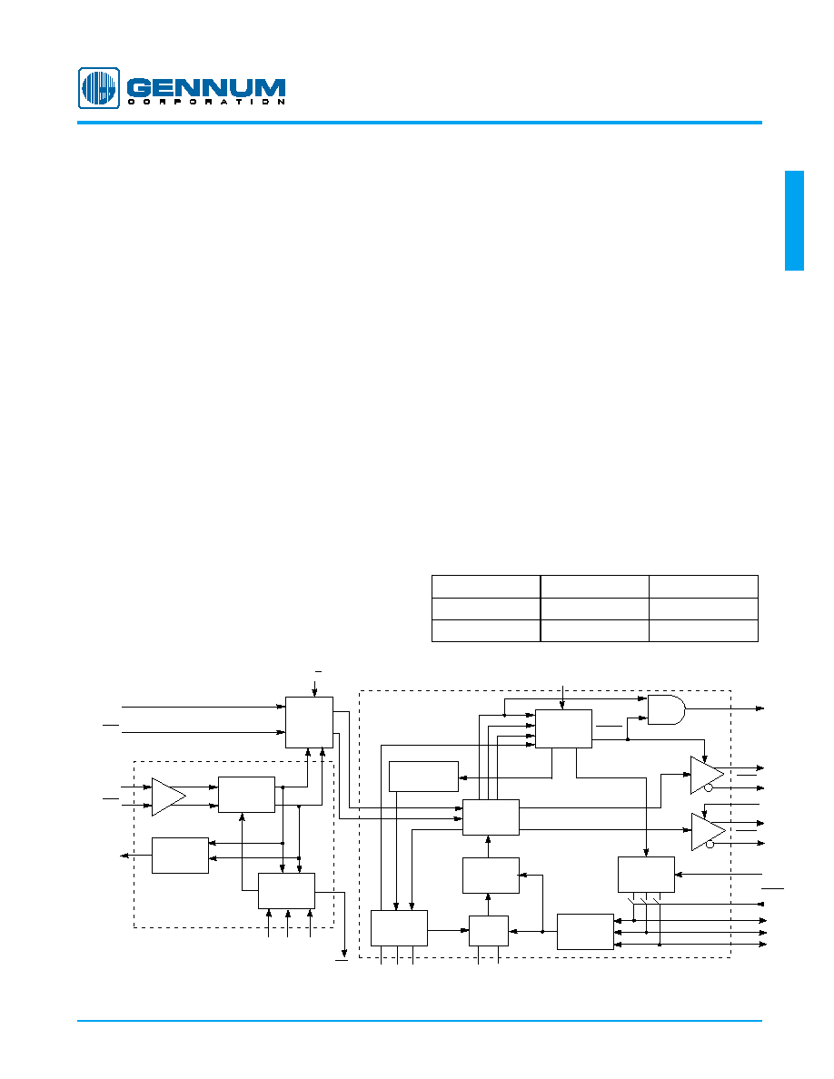
The GS9025A provides automatic cable equalization and
high performance clock and data recovery for serial digital
signals. The GS9025A receives either single-ended or
differential serial digital data and outputs differential clock
and retimed data signals at PECL levels (800mV). The on-
board cable equalizer provides up to 40dB of gain at
200MHz which typically results in equalization of greater
than 350m of high quality cable at 270Mb/s.
The GS9025A operates in either auto or manual data rate
selection mode. In both modes, the GS9025A requires only
one external resistor to set the VCO centre frequency and
provides adjustment free operation.
The GS9025A has dedicated pins to indicate signal
strength/carrier detect, LOCK and data rate. Optional
external resistors allow the carrier detect threshold level to
be customized to the user's requirement. In addition, the
GS9025A provides an 'Output Eye Monitor Test'
(OEM_TEST) for diagnostic testing of signal integrity after
equalization, prior to reslicing. The serial clock outputs can
also be disabled to reduce power. The GS9025A operates
from a single +5 or -5 volt supply.
BLOCK DIAGRAM
ORDERING INFORMATION
PART NUMBER
PACKAGE
TEMPERATURE
GS9025ACQM
44 pin MQFP Tray
0∞C to 70∞C
GS9025ACTM
44 pin MQFP Tape
0∞C to 70∞C
LF+ LFS LF-
CBG R
VCO
CARRIER DETECT
PHASELOCK
HARMONIC
FREQUENCY
ACQUISITION
VCO
DIVISION
3 BIT
COUNTER
LOCK
SDO
SDO
CLK_EN
SCO
SCO
SMPTE
AUTO/MAN
SS0
SS1
SS2
MUTE
C
OSC
A/D
PHASE
DETECTOR
DECODER
LOGIC
ANALOG
DIGITAL
MUX
DDI
+
-
DDI
SDI
SDI
OEM_TEST
AGC CAP CD_ADJ
AUTO EQ
CONTROL
EYE
MONITOR
VARIABLE
GAIN EQ
STAGE
CHARGE
PUMP
+
-
+ -
SSI/CD
GENLINX
TM
II
GS9025A
Serial Digital Receiver
GENNUM CORPORATION
522 - 75 - 00
2
G
S
9
025
A
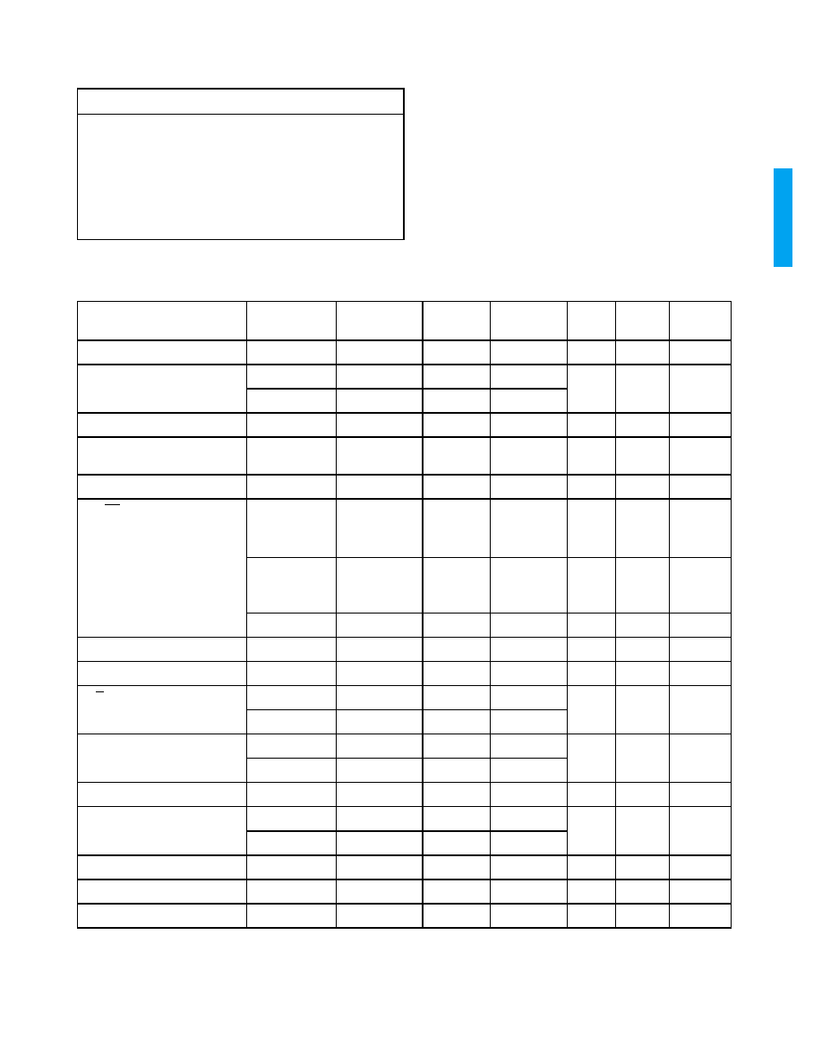
ABSOLUTE MAXIMUM RATINGS
PARAMETER
VALUE
Supply Voltage (V
S
)
5.5V
Input Voltage Range (any input)
V
CC
+ 0.5 to V
EE
- 0.5V
Operating Temperature Range
0∞C
T
A
70∞C
Storage Temperature Range
-65∞C
T
S
150∞C
Lead Temperature (soldering, 10 sec)
260∞C
DC ELECTRICAL CHARACTERISTICS
V
CC
= 5.0V, T
A
= 25∞C unless otherwise stated, R
LF
= 1.8k, C
LF1
= 15nF, C
LF2
= 3.3pF
PARAMETER
CONDITION
MIN
TYPICAL
1
MAX
UNITS
NOTES
TEST
LEVEL
Supply Voltage
4.75
5
5.25
V
1
Supply Current
CLK_EN = 0
-
115
mA
1
CLK_EN = 1
-
125
SDI Common Mode Voltage
-
2.5
-
V
1
DDI Common Mode Input
Voltage Range
V
EE
+(V
DIFF
/2)
0.4 to 4.6
V
CC
-(V
DIFF
/2)
V
2
1
DDI Differential Input Drive
200
800
2000
mV
1
SSI/CD Output Current
Source,
C
LMAX
= 50pF,
R
L
= open cct.
-
-
18
µA
3
Source,
C
LMAX
= 50pF,
R
L
=5K
-
-
110
µA
3
Sink
-
1.0
1.5
mA
3
AGC Common Mode Voltage
-
2.7
-
V
1
OEM_TEST Bias Potential
-
4.5
-
V
5
1
A/D, AUTO/MAN, SMPTE,
SS[2:0] Input Voltage
High
2.0
-
-
V
1
Low
-
-
0.8
CLK_EN Input Voltage
High
2.5
-
-
V
1
Low
-
-
0.8
LOCK Output Sink Current
500
-
-
µA
3
1
SS[2:0] Output Voltage
High
4.4
4.7
-
V
1
Low
-
0.2
0.4
SS[2:0] Source Current
Auto Mode
180
300
-
µA
1
SS[2:0] Sink Current
Auto Mode
0.6
1.0
-
mA
SS[2:0] Source Current
Manual Mode
-
0
-
µA
4
1
GENNUM CORPORATION
522 - 75 - 00
3
G
S
9
025
A
SS[2:0] Sink Current
Manual Mode
-
0.8
5
µA
CLK_EN Source Current
Low
-
26
55
µA
1
NOTES
1. TYPICAL - measured on EB9025A board.
2. V
DIFF
is the differential input signal swing.
3. LOCK is an open collector output and requires an external pullup
resistor.
4. Pins SS[2:0] are outputs in AUTO mode and inputs in MANUAL
mode.
5. If OEM_TEST is permanently enabled, operating temperature
range is limited from 0∞C to 60∞C inclusive.
TEST LEVELS
1. Production test at room temperature and nominal supply
voltage with guardbands for supply and temperature
ranges.
2. Production test at room temperature and nominal supply
voltage with guardbands for supply and temperature
ranges using correlated test.
3. Production test at room temperature and nominal supply
voltage.
4. QA sample test.
5. Calculated result based on Level 1,2, or 3.
6. Not tested. Guaranteed by design simulations.
7. Not tested. Based on characterization of nominal parts.
8. Not tested. Based on existing design/characterization
data of similar product.
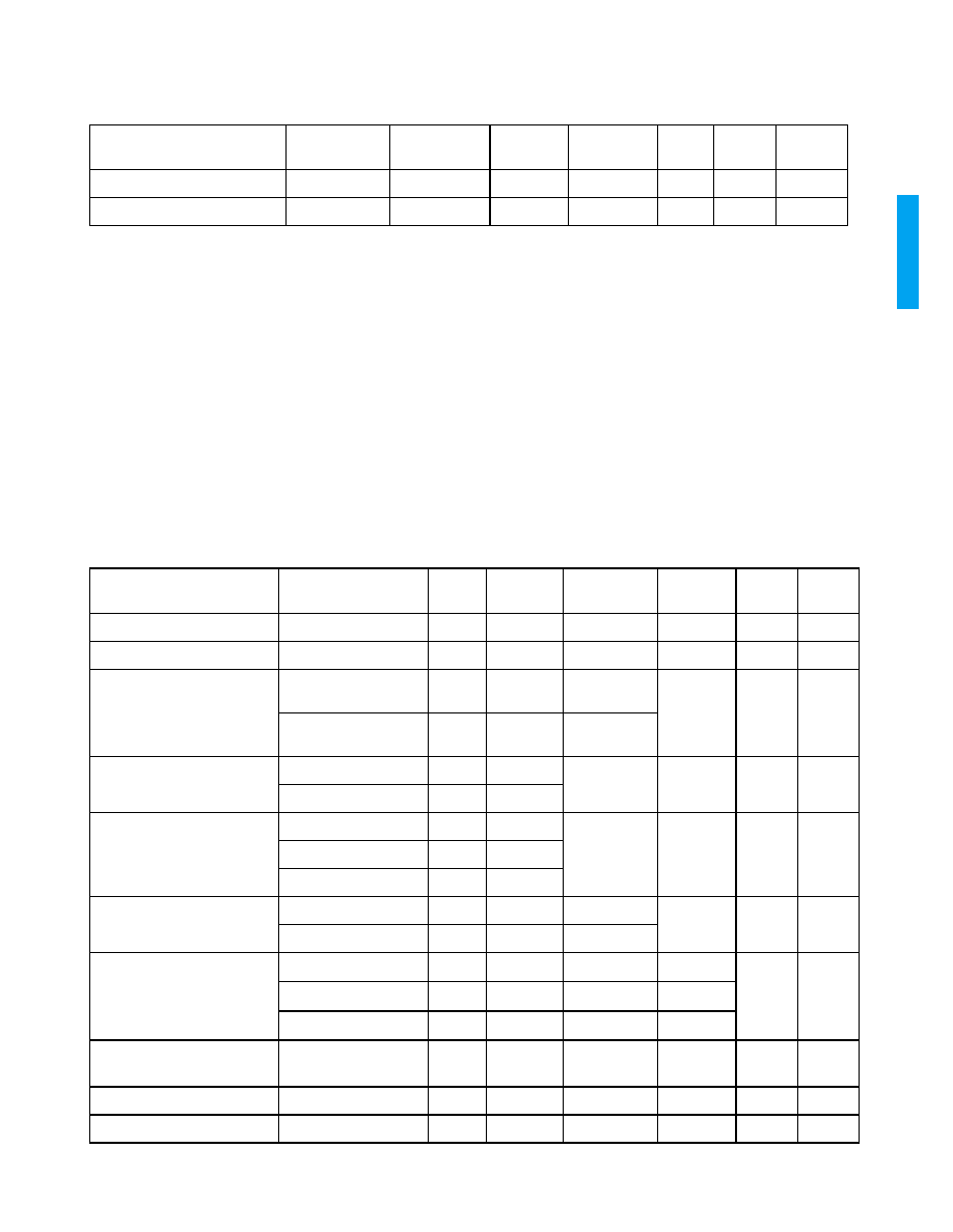
AC ELECTRICAL CHARACTERISTICS
V
CC
= 5.0V, V
EE
= 0V, T
A
= 25∞C unless otherwise stated, R
LF
= 1.8k, C
LF1
= 15nF, C
LF2
= 3.3pF
PARAMETER
CONDITIONS
MIN
TYPICAL
1
MAX
UNITS
NOTES
TEST
LEVEL
Serial Data Rate
SDI
143
-
540
Mb/s
1
Maximum Equalizer Gain
@ 200MHz
-
40
-
dB
7
Additive Jitter
[Pseudorandom (2
23
-1)]
270Mb/s, 300m
(Belden 8281)
-
300
-
ps p-p
2, 8
3
540Mb/s, 100m
(Belden 8281)
-
275
-
Intrinsic Jitter
[Pseudorandom (2
23
-1)]
270Mb/s
-
185
see Figure 12
ps p-p
2, 7
4
540Mb/s
-
164
Intrinsic Jitter
[Pathological (SDI checkfield)]
270Mb/s
-
462
see Figure 13
ps p-p
2, 7
1
360Mb/s
-
308
540Mb/s
-
260
Input Jitter Tolerance
270Mb/s
0.40
0.56
-
UI p-p
3, 7
1
540Mb/s
0.35
0.43
-
Lock Time -
Synchronous Switch
t
switch
< 0.5µs, 270Mb/s
-
1
-
µs
4
7
0.5µs< t
switch
<10ms
-
1
-
ms
t
switch
> 10 ms
-
4
-
ms
Lock Time -
Asynchronous Switch
Loop Bandwidth
= 6MHz @ 540Mb/s
-
10
-
ms
5
7
Carrier Loss Time
0.5
1
2
µs
6
7
SDO to SCO Synchronization
-200
0
200
ps
7
DC ELECTRICAL CHARACTERISTICS (continued)
V
CC
= 5.0V, T
A
= 25∞C unless otherwise stated, R
LF
= 1.8k, C
LF1
= 15nF, C
LF2
= 3.3pF
PARAMETER
CONDITION
MIN
TYPICAL
1
MAX
UNITS
NOTES
TEST
LEVEL

GENNUM CORPORATION
522 - 75 - 00
4
G
S
9
025
A
Fig. 1 Test Setup for Figures 6 - 13
SDO, SCO Output Signal
Swing
75
DC load
600
800
1000
mV p-p
1
SDO, SCO Rise & Fall times
20%-80%
200
300
400
ps
7
SDI/SDI Input Resistance
-
10
-
k
8
6
SDI/SDI Input Capacitance
-
1.0
-
pF
8
6
SDI/SDI Input Return Loss
at 270MHz
15
20
-
dB
8
6
Carrier Detect Response Time
Carrier Applied,
C
L
<50pF, R
L
=open cct.
-
3
-
µs
8
6
Carrier Removed,
C
L
<50pF, R
L
=open cct.
-
30
-
NOTES
1. TYPICAL - measured on EB9025A board.
2. Characterized 6 sigma rms.
3. IJT measured with sinusoidal modulation beyond Loop
Bandwidth (at 6.5MHz).
4. Synchronous switching refers to switching the input data from
one source to another source which is at the same data rate (ie.
line 10 switching for component NTSC).
5. Asynchronous switching refers to switching the input data from
one source to another source which is at a different data rate.
6. Carrier Loss Time refers to the response of the SDO output from
valid re-clocked input data to mute mode when the input signal
is removed.
7. Using the DDI input, A/D=0.
8. Using the SDI input, A/D=1.
TEST LEVELS
1. Production test at room temperature and nominal supply
voltage with guardbands for supply and temperature
ranges.
2. Production test at room temperature and nominal supply
voltage with guardbands for supply and temperature ranges
using correlated test.
3. Production test at room temperature and nominal supply
voltage.
4. QA sample test.
5. Calculated result based on Level 1,2, or 3.
6. Not tested. Guaranteed by design simulations.
7. Not tested. Based on characterization of nominal parts.
8. Not tested. Based on existing design/characterization data
of similar product.
AC ELECTRICAL CHARACTERISTICS
V
CC
= 5.0V, V
EE
= 0V, T
A
= 25∞C unless otherwise stated, R
LF
= 1.8k, C
LF1
= 15nF, C
LF2
= 3.3pF
PARAMETER
CONDITIONS
MIN
TYPICAL
1
MAX
UNITS
NOTES
TEST
LEVEL
EB9025A
BOARD
GS9028
CABLE
DRIVER
TEKTRONIX
GigaBERT
1400
ANALYZER
TEKTRONIX
GigaBERT
1400
TRANSMITTER
BELDEN 8281
CABLE
DATA
DATA
CLOCK
TRIGGER

GENNUM CORPORATION
522 - 75 - 00
5
G
S
9
025
A
PIN CONNECTIONS
PIN DESCRIPTIONS
NUMBER
SYMBOL
TYPE
DESCRIPTION
1, 2
DDI/DDI
I
Digital data inputs (Differential ECL/PECL).
3, 44
V
CC
_75
I
Power supply connection for internal 75
pullup resistors connected to DDI/DDI.
4, 8, 13, 22, 35
V
CC
I
Most positive power supply connection.
5, 9, 14, 18, 27,
30, 33, 34, 37
V
EE
I
Most negative power supply connection.
6, 7
SDI/SDI
I
Differential analog data inputs.
10
CD_ADJ
I
Carrier detect threshold adjust.
11, 12
AGC-, AGC+
I
External AGC capacitor.
15
LF+
I
Loop filter component connection.
16
LFS
I
Loop filter component connection.
17
LF-
I
Loop filter component connection.
19
R
VCO
_RTN
I
Frequency setting resistor return connection.
20
R
VCO
I
Frequency setting resistor connection.
21
CBG
I
Internal bandgap voltage filter capacitor.
23, 24, 25
SS[2:0]
I/O
Data rate indication (auto mode) or data rate select (manual mode). TTL/CMOS
compatible I/O. In auto mode, these pins can be left unconnected.
26
AUTO/MAN
I
Auto or manual mode select. TTL/CMOS compatible input.
SDO
SDO
V
EE
SCO
SCO
V
EE
AUTO/MAN
SS0
SS1
SS2
GS9025A
TOP VIEW
AGC+
V
CC
V
EE
LF+
LFS
LF-
V
EE
R
VCO
_RTN
R
VCO
CBG
V
CC
DDI
DDI
V
CC
_75
V
CC
V
EE
SDI
SDI
V
CC
V
EE
CD_ADJ
AGC-
V
CC
_75
OEM_TEST
SMPTE
A/D
SSI/CD
LOCK
C
OSC
V
EE
CLK_EN
V
CC
V
EE
V
EE
1
2
3
4
5
6
7
8
9
10
11
33
32
31
30
29
28
27
26
25
24
23
12
13
14
15
16
17
18 19
20
21 22
44
43
42
41
40
39
38 37
36
35 34