 | –≠–ª–µ–∫—Ç—Ä–æ–Ω–Ω—ã–π –∫–æ–º–ø–æ–Ω–µ–Ω—Ç: GS9035A | –°–∫–∞—á–∞—Ç—å:  PDF PDF  ZIP ZIP |
GENNUM CORPORATION P.O. Box 489, Stn. A, Burlington, Ontario, Canada L7R 3Y3
Tel. +1 (905) 632-2996 Fax. +1 (905) 632-5946 E-mail: info@gennum.com
www.gennum.com
Revision Date: June 2004
Document No. 522 - 41 - 08
DATA SHEET
GS9
035
A
FEATURES
∑ adjustment-free operation
∑ auto-rate selection for 5 SMPTE data rates: 143, 177,
270, 360, 540Mb/s
∑ data rate indication output
∑ serial data output mute when PLL is not locked
∑ immune to harmonic locking
∑ operation independent of SAV/EAV sync signals
∑ low jitter, low power
∑ single external VCO resistor for operation with five
input data rates
∑ large input jitter tolerance: typically 0.45 UI beyond
loop bandwidth
∑ power savings mode (output serial clock disable)
∑ system friendly: serial clock remains active when data
outputs muted
∑ robust lock detect
∑ Pb-free and Green
APPLICATIONS
The GS9035A is used for Clock and Data recovery, and
Jitter elimination for all high speed serial digital interface
applications involving SMPTE 259M and other data
standards.
DESCRIPTION
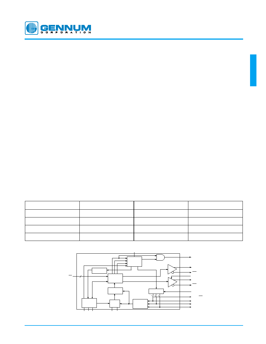
The GS9035A is a high performance clock and data
recovery IC designed for serial digital data. The GS9035A
receives either single-ended or differential PECL data and
outputs differential PECL clock and retimed data signals.
The GS9035A can operate in either auto or manual rate
selection mode. In auto mode the GS9035A is ideal for
multi-rate serial data protocols such as SMPTE 259M. In this
mode the GS9035A automatically detects and locks onto
the incoming data signal. For single rate data systems, the
GS9035A can be configured to operate in manual mode. In
both modes, the GS9035A requires only one external
resistor to set the VCO centre frequency and provides
adjustment-free operation.
The GS9035A has dedicated pins to indicate LOCK and
data rate. In addition, an internal muting function forces the
serial data outputs to a static state when input data is not
present or when the PLL is not locked. The serial clock
outputs can also be disabled resulting in a 10% power
savings.
The GS9035A is packaged in a 28 pin PLCC and operates
from a single +5 or -5 volt power supply.
BLOCK DIAGRAM
ORDERING INFORMATION
PART NUMBER
PACKAGE
TEMPERATURE
Pb-FREE AND GREEN
GS9035ACPJ
28 pin PLCC
0∞C to 70∞C
No
GS9035ACTJ
28 pin PLCC Tape
0∞C to 70∞C
No
GS9035ACPJE3
28 pin PLCC
0∞C to 70∞C
Yes
GS9035ACTJE3
28 pin PLCC Tape
0∞C to 70∞C
Yes
DDI/DDI
LF+ LFS LF-
CBG R
VCO
CARRIER DETECT
PHASELOCK
HARMONIC
FREQUENCY
ACQUISITION
VCO
DIVISION
3 BIT
COUNTER
LOCK
SDO
SDO
CLK_EN
SCO
SCO
SMPTE
AUTO/MAN
SSO
SS1
SS2
2
PHASE
DETECTOR
CHARGE
PUMP
DECODER
LOGIC
C
OSC
GENLINX
TM
II
GS9035A
Serial Digital Reclocker
GENNUM CORPORATION
522 - 41 - 08
2 of 14
GS9
035
A
ABSOLUTE MAXIMUM RATINGS
PARAMETER
VALUE
Supply Voltage (V
S
) 5.5V
Input Voltage Range (any input)
V
CC
+ 0.5 to V
EE
- 0.5V
Operating Temperature Range
0∞C
T
A
70∞C
Storage Temperature Range
-65∞C
T
S
150∞C
Lead Temperature (soldering, 10 sec)
260∞C
DC ELECTRICAL CHARACTERISTICS
V
CC
= 5.0V, V
EE
= 0V, T
A
= 0∞ ≠ 70∞C unless otherwise stated, R
LF
= 1.8K, C
LF1
= 15nF, C
LF2
= 3.3pF.
PARAMETER
CONDITION
MIN
TYPICAL
1
MAX
UNITS
NOTES
TEST
LEVEL
Supply Voltage
4.75
5.00
5.25
V
3
Supply Current
CLK_EN = 0
-
90
110
mA
3
CLK_EN = 1
-
105
120
mA
3
DDI/DDI Common Mode Input
Voltage Range
V
EE
+ (V
DIFF
/2)
0.4 to 4.6
V
CC
- (V
DIFF
/2)
V
2
3
DDI/DDI Differential Input
Drive
200
800
2000
mV
3
AUTO/MAN, SMPTE
High
2.0
-
-
V
3
Low
-
-
0.8
CLK_EN Input Voltage
High
2.5
-
-
V
3
Low
-
-
0.8
LOCK Output Low Voltage
OH
=
500µA
-
0.25
0.4
V
3
1
SS{2:0} Output Voltage
HIGH,
OH
= -180µA,
Auto Mode
4.4
4.8
-
V
1
LOW,
OL
=
600µA,
Auto Mode
-
0.3
0.4
SS{2:0} Input Voltage
HIGH, Manual Mode
2
-
-
V
3
LOW, ManualMode
-
-
0.8
CLK_EN Source Current
Low, V
IL
= 0V
-
26
55
µA
1
NOTES
1. TYPICAL - measured on EB-RD35A board.
2. V
DIFF
is the differential input signal swing.
3. LOCK is an open collector output and requires an
external pull-up resistor.
4. Pins SS[2:0] are outputs in AUTO mode and inputs in
MANUAL mode.
TEST LEVELS
1. Production test at room temperature and nominal supply
voltage with guardbands for supply and temperature ranges.
2. Production test at room temperature and nominal supply
voltage with guardbands for supply and temperature ranges
using correlated test.
3. Production test at room temperature and nominal supply
voltage.
4. QA sample test.
5. Calculated result based on Level 1,2, or 3.
6. Not tested. Guaranteed by design simulations.
7. Not tested. Based on characterization of nominal parts.
GENNUM CORPORATION
522 - 41 - 08
3 of 14
GS9
035
A
AC ELECTRICAL CHARACTERISTICS
V
CC
= 5.0V, V
EE
= 0V, T
A
= 0∞ ≠ 70∞C unless otherwise stated, R
LF
= 1.8K, C
LF1
= 15nF, C
LF2
= 3.3pF
PARAMETER
CONDITION
MIN
TYPICAL
1
MAX
UNITS
NOTES
TEST
LEVEL
Serial Data Rate
SDI
143
-
540
Mb/s
3
Intrinsic Jitter
Psuedorandom (2
23
- 1)
270Mb/s
-
185
See Figure 6
ps p-p
2
4
540Mb/s
-
164
Intrinsic Jitter
Pathological
(SDI checkfield)
270Mb/s
-
462
See Figure 7
ps p-p
2
3
360Mb/s
-
308
540Mb/s
-
260
Input Jitter Tolerance
270Mb/s
0.40
0.56
-
UI p-p
3
9
540Mb/s
0.35
0.43
-
Lock Time Synchronous
Switch
t
SWITCH
< 0.5µs, 270Mb/s
-
1
-
µs
4
7
0.5µs < t
SWITCH
< 10ms
-
1
-
ms
t
SWITCH
> 10ms
-
4
-
ms
Lock Time
Asynchronous Switch
Loop Bandwidth = 6MHz at 540 Mb/s
-
10
-
ms
5
7
SDO MUTE Time
0.5
1
2
µs
6
7
SDO to SCO
Synchronization
-200
0
200
ps
7
SDO, SCO Output Signal
Swing
75
DC load
600
800
1000
mV p-p
1
SDO, SCO Rise and Fall
Times
20% - 80%
200
300
400
ps
7
NOTES
1. TYPICAL - measured on EB-RD35A board, T
A
= 25∞C.
2. Characterized 6 sigma rms.
3. IJT measured with sinusoidal modulation beyond Loop Bandwidth (at 6.5MHz).
4. Synchronous switching refers to switching the input data from one source to another source which is at the same data rate (ie: line 10
switching for component NTSC).
5. Asynchronous switching refers to switching the input data from one source to another source which is at a different data rate.
6. SDO MUTE Time refers to the response of the SDO output from valid re-clocked input data to mute mode when the input signal is removed.
TEST LEVEL
1. Production test at room temperature and nominal supply voltage with guardbands for supply and temperature ranges.
2. Production test at room temperature and nominal supply voltage with guardbands for supply and temperature ranges using correlated
test.
3. Production test at room temperature and nominal supply voltage.
4. QA sample test.
5. Calculated result based on Level 1,2, or 3.
6. Not tested. Guaranteed by design simulations.
7. Not tested. Based on characterization of nominal parts.
8. Not tested. Based on existing design/characterization data of similar product.
9. Indirect test
GENNUM CORPORATION
522 - 41 - 08
4 of 14
GS9
035
A
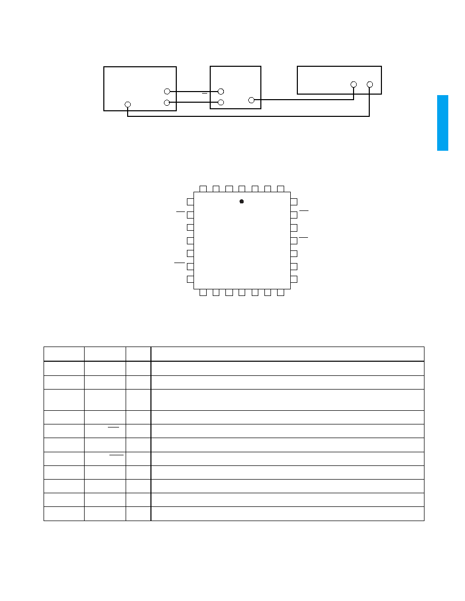
Fig. 1 Jitter Measurement Test Setup
PIN CONNECTIONS
PIN DESCRIPTIONS
NUMBER
SYMBOL
TYPE
DESCRIPTION
1,7,8,11,27
V
EE
I
Most negative power supply connection.
2
COSC
I
Timing control capacitor for internal system clock.
3
LOCK
O
Lock indication. When HIGH, the GS9035A is locked. LOCK is an open collector output and
requires an external 10k pullup resistor.
4
SMPTE
I
SMPTE/Other rate select.
5, 6
DDI/DDI
I
Digital data input (Differential ECL/PECL).
9
V
CC1
I
Most positive power supply connection.
10
AUTO/MAN
I
Auto or Manual mode select. TTL/CMOS compatible input.
12
LF+
I
Loop filter component connection.
13
LFS
I
Loop filter component connection.
14
LF-
I
Loop filter component connection.
15
R
VCO
_RTN
I
R
VCO
return.
PATTERN 2
23
-1
CLK DATA
DI
DI
SDO
CH-1 TRIG
TEKTRONIX
GIGABERT 1400
GENNUM
TEST BOARD
TEKTRONIX
CSA803
DDI
DDI
V
EE
V
EE
V
CC1
AUTO/MAN
V
EE
SDO
SDO
SCO
SCO
SSO
SS1
SS2
SMPTE
LOCK
COSC
V
EE
CLK_EN
V
EE
V
CC3
GS9035A
TOP VIEW
LF+
LFS
LF-
R
VCO
_RTN
R
VCO
CBG
V
CC2
25
24
23
22
21
20
19
5
6
7
8
9
10
11
12 13 14 15 16 17 18
4 3 2 1 28 27 26
GENNUM CORPORATION
522 - 41 - 08
5 of 14
GS9
035
A
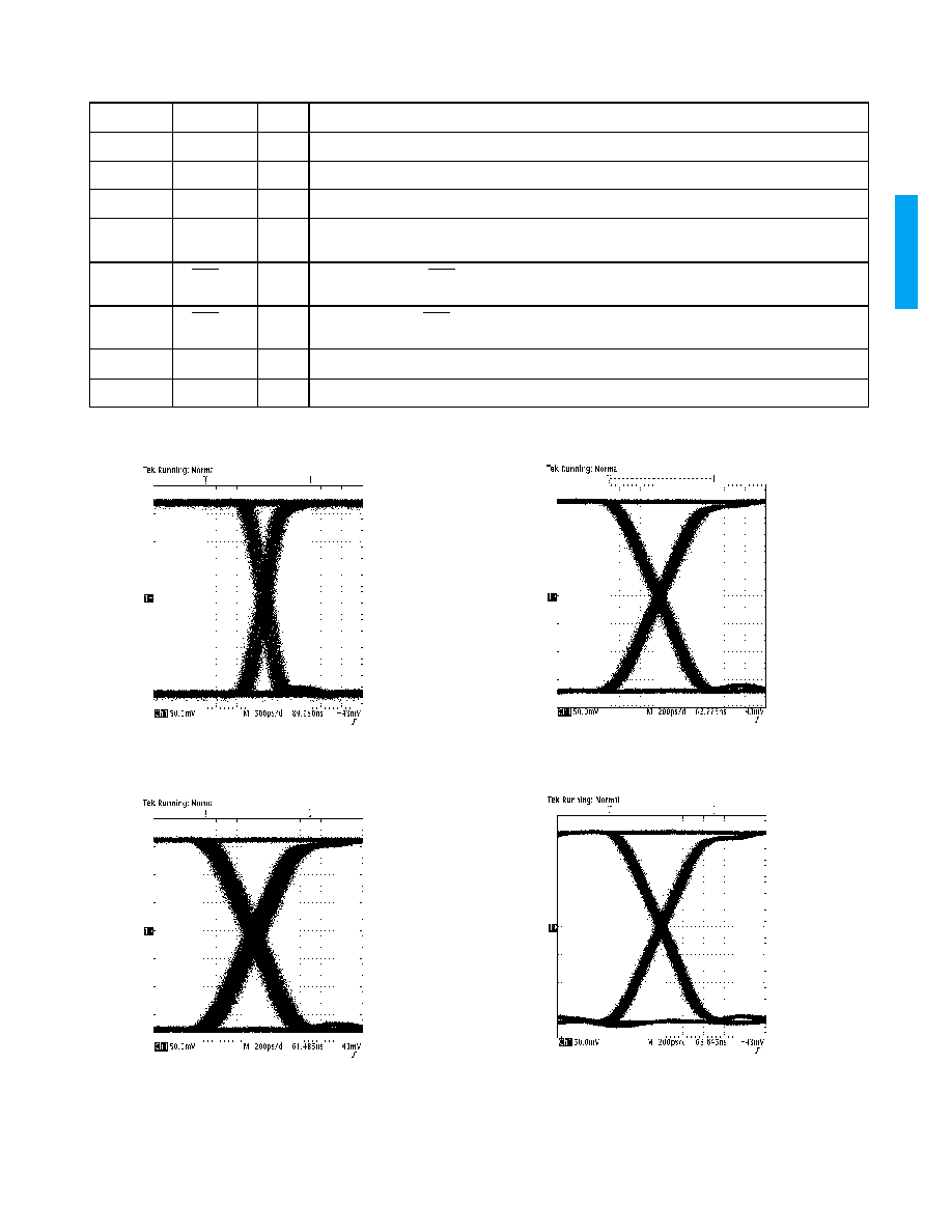
TYPICAL PERFORMANCE CURVES
(V
S
= 5V, T
A
= 25∞C unless otherwise shown.)
Fig. 2 Intrinsic Jitter (2
23
-1 Pattern) 30Mb/s
Fig. 3 Intrinsic Jitter (2
23
-1 Pattern) 143Mb/s
Fig. 4 Intrinsic Jitter (2
23
-1 Pattern) 270Mb/s
Fig. 5 Intrinsic Jitter (2
23
-1 Pattern) 540Mb/s
16
R
VCO
I
Frequency setting resistor.
17
CBG
I
Internal bandgap voltage filter capacitor.
18
V
CC2
I
Most positive power supply connection.
19 - 21
SS[2:0]
I/O
Data rate indication (Auto mode) or data rate select (Manual mode). TTL/CMOS compatible I/O. In
auto mode these pins can be left unconnected.
22, 23
SCO/SCO
O
Serial clock output. SCO/SCO are differential current mode outputs and require external 75
pullup resistors.
24, 25
SDO/SDO
O
Serial data output. SDO/SDO are differential current mode outputs and require external 75
pullup
resistors.
26
V
CC3
I
Most positive power supply connection.
28
CLK_EN
I
Clock enable. When HIGH, the serial clock outputs are enabled.
PIN DESCRIPTIONS
(continued)
NUMBER
SYMBOL
TYPE
DESCRIPTION