www.gennum.com
GS9074A HD-LINXÆ II
Adaptive Cable Equalizer
GS9074A Data Sheet
34166 - 3
March 2006
1 of 16
Features
∑
SMPTE 259M compliant
∑
Automatic cable equalization
∑
Multi-standard operation from 143Mb/s to 360Mb/s
∑
Supports DVB-ASI at 270Mb/s
∑
Small footprint (4mm x 4mm)
∑
Pb-free and RoHS compliant
∑
Manual bypass (useful for low data rates with slow
rise/fall times)
∑
Performance optimized for 270Mb/s
∑
Typical maximum equalized length of Belden
1694A cable: 350m at 270Mb/s
∑
50
differential output (with internal 50 pull-ups)
∑
Manual output mute or programmable mute based
on max cable length adjust
∑
Single 3.3V power supply operation
∑
Operating temperature range: 0∞C to +70∞C
Applications
∑
SMPTE 259M Coaxial Cable Serial Digital
Interfaces.
Description
The GS9074A is a second-generation high-speed
BiCMOS integrated circuit designed to equalize and
restore signals received over 75
co-axial cable.
The GS9074A is designed to support SMPTE 259M,
and is optimized for performance at 270Mb/s.
The GS9074A features DC restoration to compensate
for the DC content of SMPTE pathological test patterns.
A voltage programmable mute threshold (MCLADJ) is
included to allow muting of the GS9074A output when
an approximate selected cable length is reached for
SMPTE 259M signals. This feature allows the GS9074A
to distinguish between low amplitude SD-SDI signals
and noise at the input of the device. The serial digital
outputs of the GS9074A may be forced to a mute state
by applying a voltage to the MUTE pin.
Power consumption is typically 215mW using a 3.3V
power supply. The GS9074A is lead-free, and the
encapsulation compound does not contain halogenated
flame retardant (RoHS compliant).
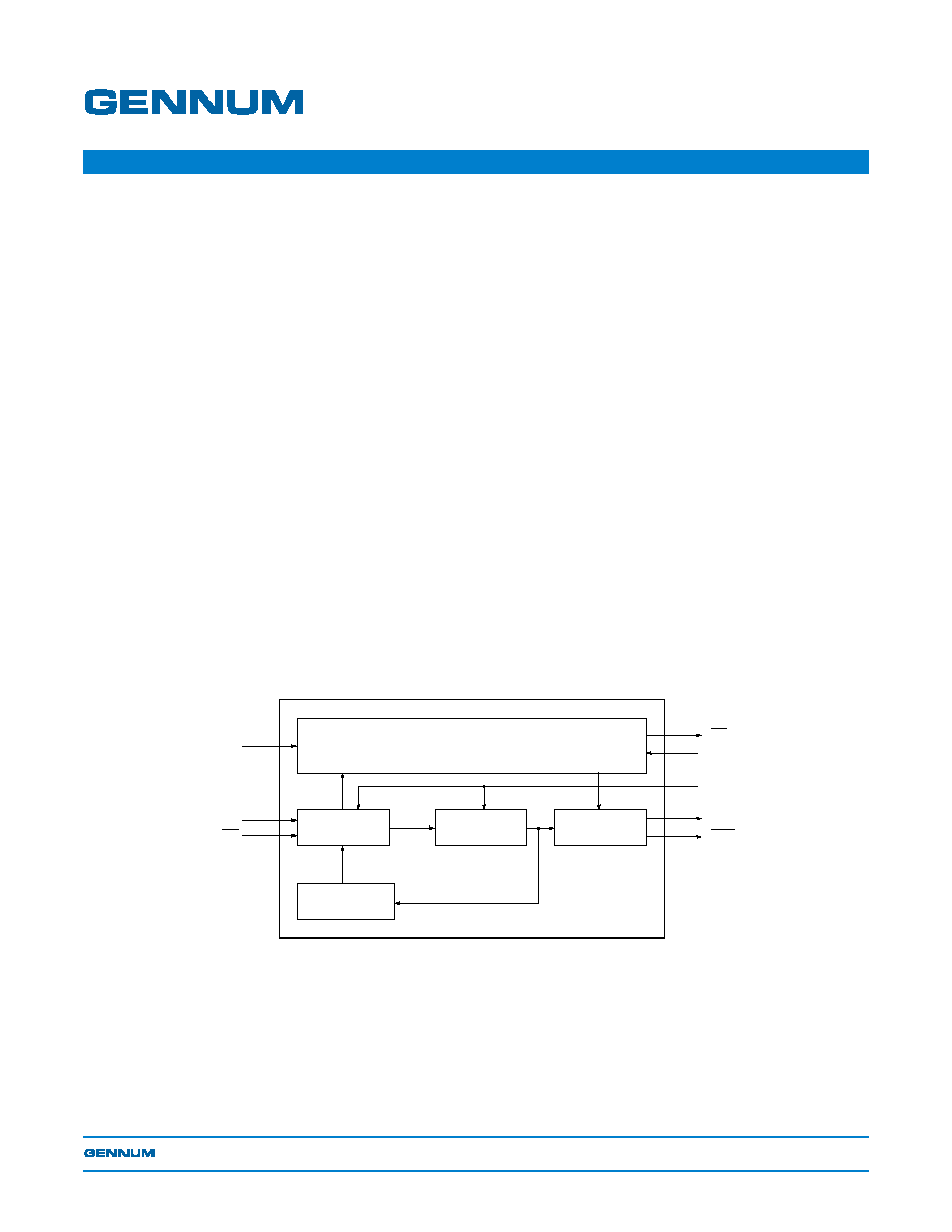
Functional Block Diagram
CABLE LENGTH ADJUSTOR
CARRIER DETECT
MUTE
EQUALIZER
DC RESTORE
OUTPUT
AGC
CD
MUTE
SDO
BYPASS
SDO
SDI
SDI
MCLADJ

GS9074A Data Sheet
34166 - 3
March 2006
2 of 16
Contents
Features ........................................................................................................................1
Applications...................................................................................................................1
Description ....................................................................................................................1
1. Pin Out ......................................................................................................................3
1.1 GS9074A Pin Assignment ..............................................................................3
1.2 GS9074A Pin Descriptions .............................................................................3
2. Electrical Characteristics...........................................................................................5
2.1 Absolute Maximum Ratings ............................................................................5
2.2 DC Electrical Characteristics ..........................................................................5
2.3 AC Electrical Characteristics ...........................................................................6
2.4 Solder Reflow Profiles .....................................................................................7
3. Input / Output Circuits ...............................................................................................9
4. Detailed Description ................................................................................................11
4.1 Serial Digital Inputs .......................................................................................11
4.2 Cable Equalization ........................................................................................11
4.3 Programmable Mute Output ..........................................................................12
4.4 Mute and Carrier Detect ................................................................................12
5. Application Information............................................................................................13
5.1 Typical Application Circuit .............................................................................13
6. Package & Ordering Information.............................................................................14
6.1 Package Dimensions ....................................................................................14
6.2 Recommended PCB Footprint ......................................................................15
6.3 Packaging Data .............................................................................................15
6.4 Ordering Information .....................................................................................15
7. Revision History ......................................................................................................16
GS9074A Data Sheet
34166 - 3
March 2006
3 of 16
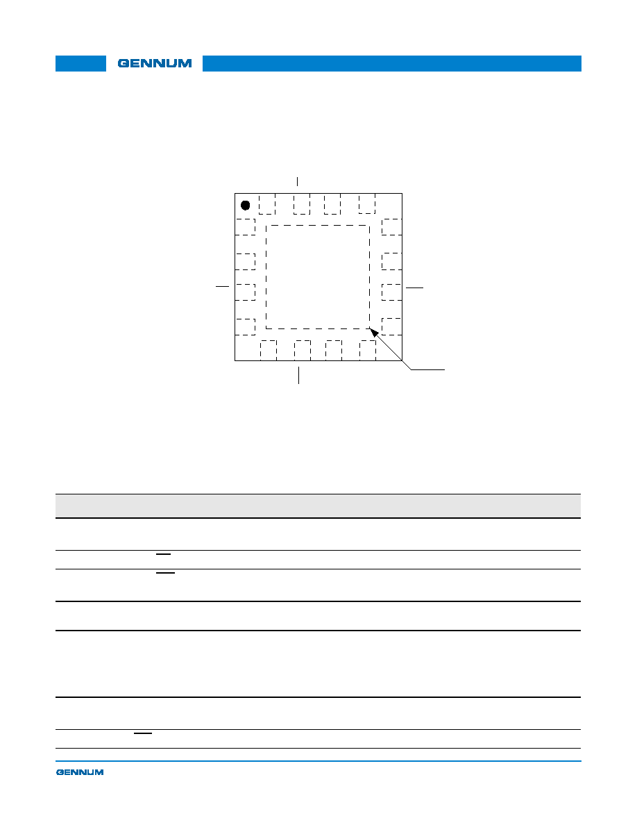
1. Pin Out
1.1 GS9074A Pin Assignment
Figure 1-1: 16-Pin QFN
1.2 GS9074A Pin Descriptions
GS9074A
(top view)
1
V
EE
_A
V
EE
_A
SDI
SDI
2
3
4
SDO
SDO
V
EE
_D
V
EE
_D
12
11
10
9
AGC
AGC
BYPASS
MCLADJ
5
7
6
8
V
CC
_A
MUTE
CD
V
CC
_D
13
14
15
16
Center Pad
(bottom of package, internally
bonded to VEE_A)
Table 1-1: GS9074A Pin Descriptions
Pin Number
Name
Timing
Type
Description
1, 4
VEE_A
Analog
Power
Most negative power supply for analog circuitry.
Connect to GND.
2, 3
SDI, SDI
Analog
Input
Serial digital differential input.
5, 6
AGC, AGC
Analog
≠
External AGC capacitors.
(See Section 5.1 Typical Application Circuit.)
7
BYPASS
Not
Synchronous
Input
Forces the Equalizing and DC RESTORE stages into bypass mode
when HIGH. No equalization occurs in this mode.
8
MCLADJ
Analog
Input
Maximum cable length adjust.
Adjusts the approximate maximum amount of cable to be equalized
(from 0m to the maximum cable length). The output is muted (latched to
the last state) when the maximum cable length is achieved.
NOTE: MCLADJ is only recommended for data rates up to 270Mb/s.
9
VEE_D
Analog
Power
Most negative power supply for the digital circuitry and output buffer.
Connect to GND.
10, 11
SDO, SDO
Analog
Output
Equalized serial digital differential output.
GS9074A Data Sheet
34166 - 3
March 2006
4 of 16
12
VEE_D
Analog
Power
Most negative power supply for the digital circuitry and output buffer.
Connect to GND.
13
VCC_D
Analog
Power
Most positive power supply for the digital I/O pins of the device.
Connect to +3.3V DC.
14
MUTE
Not
Synchronous
Input
CONTROL SIGNAL INPUT
levels are LVCMOS/LVTTL compatible. (3.3V Tolerant)
(Internal pull down resistor)
When the MUTE pin is set HIGH by the application interface, the serial
digital output of the device will be forced to a steady state.
When the MUTE pin is set LOW, the serial digital output of the device
will be active.
NOTE: This pin may be connected directly to the CD pin to allow mute
on loss of carrier.
15
CD
Not
Synchronous
Output
STATUS SIGNAL OUTPUT
Signal levels are LVCMOS/LVTTL compatible.
Indicates the presence of a good input signal.
When the CD pin is LOW, a good input signal has been detected.
When this pin is HIGH, the input signal is invalid.
This pin will indicate loss of carrier for data rates > 19Mb/s.
16
VCC_A
Analog
Power
Most positive power supply for the analog circuitry of the device.
Connect to +3.3V DC.
≠
Center Pad
≠
Power
Internally bonded to VEE_A.
Table 1-1: GS9074A Pin Descriptions (Continued)
Pin Number
Name
Timing
Type
Description
GS9074A Data Sheet
34166 - 3
March 2006
5 of 16
2. Electrical Characteristics
2.1 Absolute Maximum Ratings
2.2 DC Electrical Characteristics
Parameter
Value
Supply Voltage
-0.5V to +3.6 V
DC
Input ESD Voltage
2kV
Storage Temperature Range
-50∞C < T
s
< 125∞C
Input Voltage Range (any input)
-0.3 to (V
CC
+0.3)V
Operating Temperature Range
0∞C to 70∞C
Reflow Temperature
260∞C
Table 2-1: DC Electrical Characteristics
V
DD
= 3.3V, T
A
= 0∞C to 70∞C, unless otherwise shown
Parameter
Symbol
Conditions
Min
Typ
Max
Units
Notes
Supply Voltage
V
CC
≠
3.135
3.3
3.465
V
±5%
Power Consumption
P
D
T
A
= 25∞C
≠
215
≠
mW
≠
Supply Current
I
s
T
A
= 25∞C
≠
65
≠
mA
≠
Output Common Mode Voltage
V
CMOUT
T
A
= 25∞C
≠
V
CC
-
V
SDO
/2
≠
V
≠
Input Common Mode Voltage
V
CMIN
T
A
= 25∞C
≠
1.75
≠
V
≠
MCLADJ DC Voltage (to mute
signal)
≠
0m, T
A
= 25∞C
≠
1.3
≠
V
≠
MCLADJ Range
≠
T
A
= 25∞C
≠
0.4
≠
V
≠
CD Output Voltage
V
CD(OH)
Carrier not
present
2.4
≠
≠
V
≠
V
CD(OL)
Carrier present
≠
≠
0.4
V
≠
Mute Input Voltage Required to
Force Outputs to Mute
V
Mute
Min to Mute
2.0
≠
≠
V
≠
Mute Input Voltage Required to
Force Outputs Active
V
Mute
Max to Activate
≠
≠
0.8
V
≠