
Document No. 521 - 20 - 02
GT4123B Two Channel
Video Multiplier
DESCRIPTION
The GT4123B is a monolithic dual-channel video multiplier
for use in a wide range of applications including broadcast
and multimedia.
Featuring two wideband video inputs and a single control
input, the GT4123B achieves broadcast quality mixing of
two video input signals to a single output by implementing
the function:
V
O
= [ ( V
C
∑ V
A
) + (1 - V
C
) ∑ V
B
]
where V
C
is the control input voltage, which may be varied
continuously over the range 0 V to 1 V, and V
A
and V
B
are
the video input signals.
The GT4123B is a low power version of the GT4123 and
GT4123A Video Multipliers which operates from ±5 V
supply voltages and typically draws only 15 mA of current.
FEATURES
two-quadrant video multiplication
operation from ±4.5 V to ±13.2 V supply voltages
20 MHz ±0.1 dB video & control channel bandwidth
ultra low differential gain & differential phase
convenient 8 pin package
Pb-free and Green
ORDERING INFORMATION
V
cc
CONTROL
FREQ. COMP
1
2
3
4
8
7
6
5
FUNCTIONAL BLOCK DIAGRAM
VIDEO IN A
OUTPUT
V
REF
(0.5V)
(INTERNAL)
FREQ
COMP
VIDEO IN B
CONTROL
MULTIPLIER
CORE
GT4123B
PIN CONNECTIONS
DATA SHEET
APPLICATIONS
∑
Multimedia Graphics Overlay
∑
Production Switchers
∑
Linear Keyers
OUTPUT
GROUND
VIDEO IN B
VIDEO IN A
V
EE
Part
Package
Temperature
Pb-Free
Number
Type
Range
and Green
GT4123BCDA
8 pin PDIP
0∞ to 70∞ C
No
GT4123BCKA
8 pin SOIC
0∞ to 70∞ C
No
GT4123BCTA
8 pin SOIC Tape
0∞ to 70∞ C
No
GT4123BCKAE3
8 pin SOIC
0∞ to 70∞ C
Yes
GENNUM CORPORATION P.O. Box 489, Stn A, Burlington, Ontario, Canada L7R 3Y3 tel. (905) 632-2996 fax: (905) 632-5946
Gennum Japan: Shinjuku Green Tower Building 27F 6-14-1, Nishi Shinjuku Shinjuku-ku, Tokyo 160-0023 Japan Tel: +81 (03) 3349-5501 Fax: +81 (03) 3349-5505
Revision date: July 2004

2 of 5
521 - 20 - 02
ELECTRICAL CHARACTERISTICS GT4123B
Supply Voltage
±V
S
±4.5
±5
±13.2
V
+ Supply Current
I+
-
15
19.5
mA
- Supply Current
I-
-
15
19.5
mA
Common Mode Input Signal
V
IN CM
Supply Voltage = ±5 V
Positve Excursion Limit
-
-
2.2
V
Negative Excursion Limit
-
-
-3.5
V
Bandwidth
BW
0.05
±0.05 dB, V
IN
= 150 mVp-p
10
-
-
MHz
BW
0.1
±0.1 dB, V
IN
= 150 mVp-p
20
25
-
MHz
Differential Gain
dg
V
IN
= 40 IRE, 0V CM
-
0.01
0.02
%
at 3.58 MHz and 4.43 MHz
Differential Phase
dp
V
IN
= 40 IRE, 0V CM
-
0.01
0.03
deg
at 3.58 MHz and 4.43 MHz
PP Signal / RMS Noise
S/N
V
SIG
= 1 Vp-p,
60
70
-
dB
Gain
A
V
100 kHz (þ = 100%)
-0.02
-0.005
-
dB
Delay
t
d
SIG
-
4
10
ns
Power Supply Rejection
PSRR
= 1 kHz
70
-
-
dB
Ratio
= 10 MHz
25
-
-
dB
Off Isolation & Crosstalk
V
A or B
/V
O
SIG
= 5 MHz (see note 1)
70
75
-
dB
V
C
/V
A or B
SIG
= 5 MHz (see note 2)
80
85
-
dB
Output Offset
Channel A or Channel B
-
-
±15
mV
Offset Difference
Channel A - Channel B
0
-
±5
mV
Input Resistance
R
IN
=1 MHz
100
-
-
k
Input Capacitance
C
IN
-
2.0
-
pF
Output Resistance
R
OUT
=1 MHz
-
-
0.50
Output Capacitance
C
OUT
-
2.0
-
pF
Bandwidth
BW
0.1
at ±0.1 dB, V
IN
= 150 mVp-p
15
20
-
MHz
Delay
t
D CONT
-
4
10
ns
Linearity
-
-
1.5
%
Control Breakthrough
V
C
= 0 to 1 V
C
=1 to 10 MHz
-
-
-35
dB
Crossfade Balance
V
C
= 0 to 1 V
C
= 3.58 MHz
-15
0
+15
mV
Control Range
V
C
0
-
+1
V
PARAMETER
SYMBOL
CONDITIONS MIN TYP MAX UNITS
POWER
SUPPLIES
SIGNAL
PATH
CONTROL
CHANNEL
ABSOLUTE MAXIMUM RATINGS
PARAMETER
VALUE/UNITS
Supply Voltage
±13.5 V
Operating Temperature Range
0∞C
T
A
70∞C
Storage Temperature Range
-65∞C
T
S
150∞C
Lead Temperature (soldering, 10 seconds)
260∞C
Video Input Voltage
±5 V
Control Input Voltage
±5 V
Video Input Differential Voltage
±5 V
CAUTION
ELECTROSTATIC
SENSITIVE DEVICES
DO NOT OPEN PACKAGES OR HANDLE
EXCEPT AT A STATIC-FREE WORKSTATION
V
S
= ±5V, T
A
= 0∞C to 70∞C, R
L
=10k
, C
L
=10pF unless otherwise shown.
NOTE:
1.
VA or B
= +1 Vp-p, output taken from OUTPUT
2 .
VC
= +1 Vp-p, output taken from VA
or
VB

3 of 5
521- 20 - 02
DETAILED DESCRIPTION
The GT4123B is a low power two quadrant video multiplier for
use in a wide range of applications including broadcast and
multimedia.
The internal topology of the device is shown in Figure 1 below.
Fig. 1 Functional Block Diagram of the GT4123B
Each input is applied to a differential amplifier (AMP A and AMP
B). From the amplifiers, the signals are passed to analog
multiplier circuits (XA and XB) whose outputs are the product
of the input signals and internally generated controlling voltages
V
CA
and V
CB
.
The internal control voltages are derived from a unity gain
differential amplifier (AMP C) whose outputs (true and invert)
are the difference between an internal 0.5 V reference voltage,
and the externally applied CONTROL voltage. In addition, the
internal DC offset of 0.5 V is applied to the controlling voltage
summing circuits
Â
2 and
Â
3.
Therefore,
V
CA
= 0.5 V + (V
C
- 0.5 V)
and
V
CB
= 0.5 V - (V
C
- 0.5 V)
When the control input V
C
equals 0.5 volts, V
CA
= 0.5 V and
V
CB
= 0.5 V, and 50% of each input signal passes to the output
of the multiplier stages.
When V
C
is less than 0.5 V, V
CA
reduces and V
CB
increases in
proportion so that less of Channel A and more of Channel B
signal is transferred. Similarly, when V
C
is greater than 0.5 V,
the opposite occurs.
The SPAN or control range is internally set so that a CONTROL
voltage of 0 V completely cuts off Channel A and fully turns on
Channel B. Similarly, a CONTROL voltage of 1 V will fully turn
on Channel A and completely turn off Channel B.
There is a small dead band at either end of the CONTROL
input. The amount of dead band is about 100 mV. The
CONTROL input can be preceded by an operational amplifier
to overcome the dead band and level shift the control signal
so that other than 0 to 1 V range can be used. The bandwidth
of the CONTROL input is in the order of 20 MHz at ±0.1 dB to
allow for very fast KEY signals.
The linear portion of the transfer characteristic has a linearity
of better than 1.5%.
The outputs from the multipliers are applied to an analog
summing circuit (
Â
1) whose output feeds a wideband amplifier
(Amp D) and presents the mixed signals to the outside world.
The inverting nodes of each input are directly connected to the
output.
In this manner, the closed loop gain is nearly unity providing
wideband, stable operation. Because the devices have only 8
pins and require virtually no external parts, the GT4123B lends
itself to high density, multi-function PC board layouts in devices
such as RGB mixers and four layer keyers where close control
law tracking is essential.
COMP
V
CA
= 0.5 + (V
C
- 0.5)
+
V
CB
OUT
AMP B
IN A
IN B
CONTROL
(V
C
)
+
+
+
V
CB
= 0.5 - (V
C
- 0.5)
+
+
-
+
AMP D
AMP C
-
+
XB
XA
-
+
AMP A
0.5V
REF
V
CA
1
2
3

4 of 5
521 - 20 - 02
0
-20
-40
-60
-80
-100
-120
FROM
NETWORK
ANALYSER
0.1
5 - 30pF
150
B
+5V
+5V
0.1
A
4
10k
4
1
3
0.1
-5V
1
7
+1V
-5V
75
8
75
TO
NETWORK
ANALYSER
8
5
CLC110
0.1
5
2
0.1
6
GT4123B
0.1 1 10
100
0.2
0.1
0
-0.1
-0.2
-0.3
-0.4
GAIN (dB)
FREQUENCY (MHz)
Fig. 4 Frequency Response
1 10
100
FREQUENCY (MHz)
Fig. 5 Crosstalk vs Frequency
V
S
= ±12V
V
S
= ±5V
VC - CHANNEL B
VC - CHANNEL A
All resistors in ohms, all capacitors in
microfarads unless otherwise stated
Fig. 2 Frequency Response, Cross Talk, Differential Gain & Phase Test Circuit
+5V
0.1
VA
VB
V
C
150
75
75
0.1
-5V
5-30 pF
6dB AMPLIFIER
VIDEO OUT
75
GT4123B
6
8
5
4
3
2
1
7
All resistors in ohms, all capacitors in
microfarads unless otherwise stated
Fig. 3 Typical Application Circuit
GT4123B TYPICAL PERFORMANCE CURVES
(V
S
= ±5V, unless otherwise specified)
CROSSTALK (dB)
5 of 5
521- 20 - 02
DOCUMENT
IDENTIFICATION
PRODUCT PROPOSAL
This data has been compiled for market investigation purposes
only, and does not constitute an offer for sale.
ADVANCE INFORMATION NOTE
This product is in a development phase and specifications are
subject to change without notice. Gennum reserves the right to
remove the product at any time. Listing the product does not
constitute an offer for sale.
PRELIMINARY DATA SHEET
The product is in a preproduction phase and specifications are
subject to change without notice.
DATA SHEET
The product is in production. Gennum reserves the right to make
changes at any time to improve reliability, function or design, in
order to provide the best product possible.
Gennum Corporation assumes no responsibility for the use of any circuits described herein and makes no representations that they are free from patent infringement.
© Copyright September 1994 Gennum Corporation. All rights reserved. Printed in Canada.
dg / dp
1 10
FREQUENCY (MHz)
Fig. 6 dg & dp vs Frequency
dg
dp
0.03
0.02
0.01
0
-0.01
-0.02
-0.03
0.1 1 10
2.5
2
1.5
1
0.5
0
Fig. 7 Output Resistance vs Frequency
FREQUENCY (MHz)
OUTPUT RESISTANCE (˝)
100
50
0
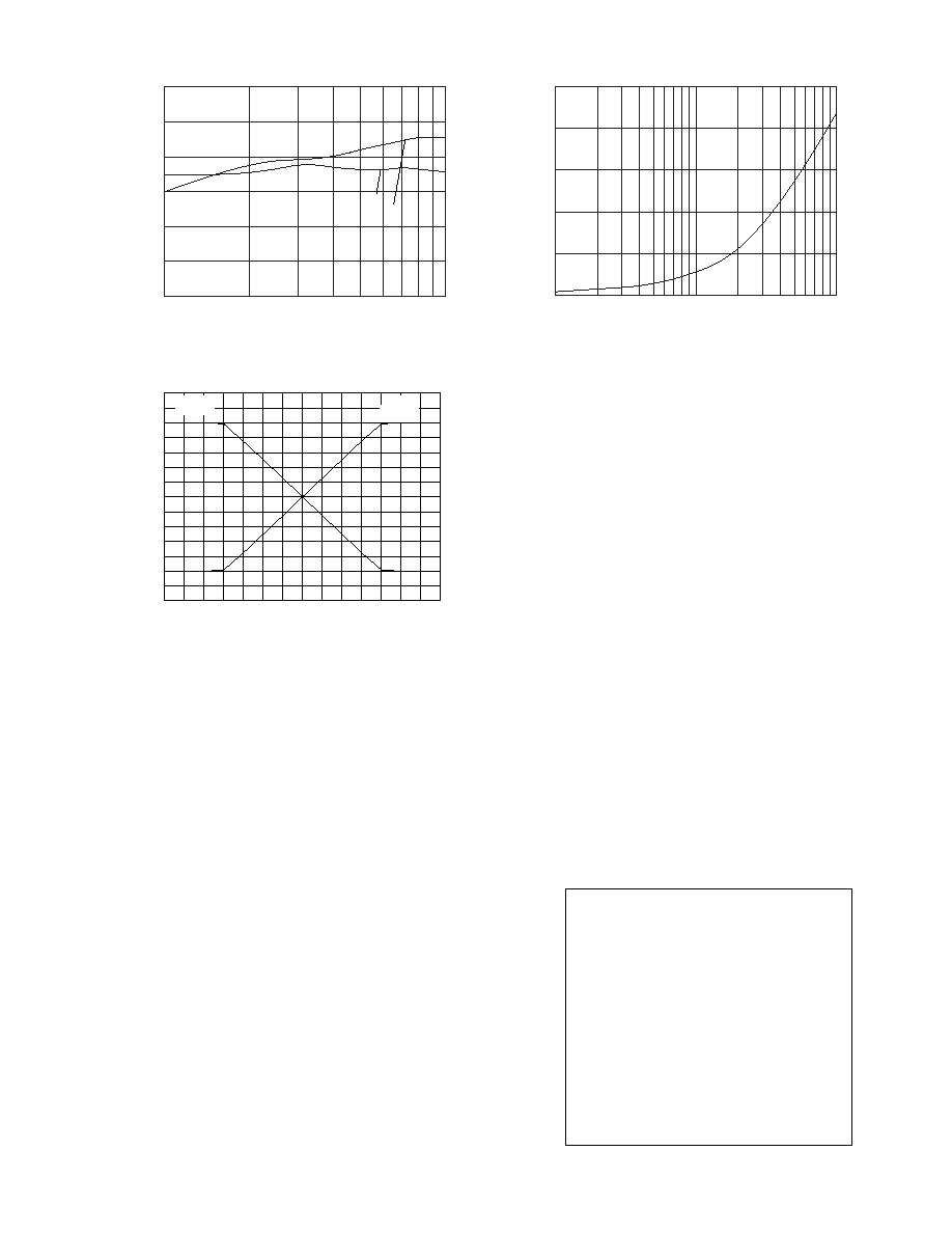
-0.2 0.0 0.2 0.4 0.6 0.8 1.0 1.2
CONTROL VOLTAGE (V
C
)
CH-B
CH-A
Fig. 8 Control Characteristics
GAIN (%)