
X
TALLY
OUT
IN
EN
Parameter
Value
Supply Voltage
±
7.5 V
Operating Temperature Range
0
∞
C
T
A
70
∞
C
Storage Temperature Range
-65
∞
C
T
S
150
∞
C
Lead Temperature
(Soldering, 10 Sec)
260
∞
C
Analog Input Voltage
-5.5 V
V
IN
5.5 V
Logic Input Voltage
-0.5 V
V
L
5.5 V
Output Load Current
12mA
High Level TALLY Output Current
2 mA
Document No. 510 - 74 - 5
GX4201 Wideband, Monolithic 1x1
Video Crosspoint Switch
CIRCUIT DESCRIPTION
The GX4201 is a wideband 1x1 video crosspoint implemented
in bipolar monolithic technology. The device is characterized
by excellent differential gain and phase in the enabled
state, and very high off-isolation in the disabled state. The
fully buffered unilateral signal path ensures negligible output
to input feedback while delivering minimal output switching
transients through make-before-break switching.
For use in NxM routing matrices, the device features a very
high, nearly constant input impedance, coupled with very
high output impedance in the disabled state. This allows
multiple GX4201's to be paralleled at the input and output
without additional circuitry. An open collector PNP to V
CC
TALLY output provides indication of crosspoint selection.
To maximize system bandwidth, an external current source
is used to bias the output device of the crosspoint. One
external current source is required per output bus. For less
demanding applications, a load resistor can be used in
place of the output current source, causing a slight increase
in differential phase. Non-additive mixing will occur on the
output bus if more than one paralleled GX4201 is enabled
at a time.
The GX4201 is one of a series of wideband video crosspoints
utilizing Gennum's proprietary LSI process.
APPLICATIONS
∑ very high quality video switching
∑ HDTV
∑ computer graphics
∑ RF switching/routing
∑ PCM/data routing
DATA SHEET
5
PIN 1
8
4
TALLY
GND
IN
GND
OUT
V
CC
V
EE
EN
8 PIN DIP
TOP VIEW
PIN CONNECTIONS
FEATURES
∑
-3 dB bandwidth, 300 MHz with C
L
= 0 pF
∑
off isolation at 100 MHz, 80 dB
∑
differential phase and gain at 4.43 MHz, 0.01
∞
&
0.02%
∑
800
µ
W disabled power consumption
∑
input signal levels from -2 V to +3 V
∑
logic input compatible with TTL and 5 V CMOS
∑
open collector TALLY output
TRUTH TABLE
EN
OUT
TALLY
0
HIGH Z
OFF
1
IN
ON
ABSOLUTE MAXIMUM RATINGS
8 PIN SOIC
1
4
5
8
EN
V
EE
V
CC
0UT
GND
IN
GND
TALLY
GENNUM CORPORATION P.O. Box 489, Stn A, Burlington, Ontario, Canada L7R 3Y3 tel. (905) 632-2996 fax: (905) 632-2055
Japan Branch: B-201 Miyamae Village, 2-10-42, Miyamae, Suginami-ku, Tokyo 168, Japan tel. (03) 3247-8838 fax (03) 3247-8839
FUNCTIONAL BLOCK DIAGRAM
PATENT PENDING
510 - 74 - 5
24
21
18
15
12
9
6
3
0
-3
-6
Gain (dB)
Phase
(degrees)
0
-0.3
-0.6
-0.9
-1.2
-1.5
-1.8
-2.1
-2.4
-2.7
-3.0
1
2
3
4
5 6 7 8 9 10
1
10
100
1K
Frequency (MHz)
Frequency (MHz)
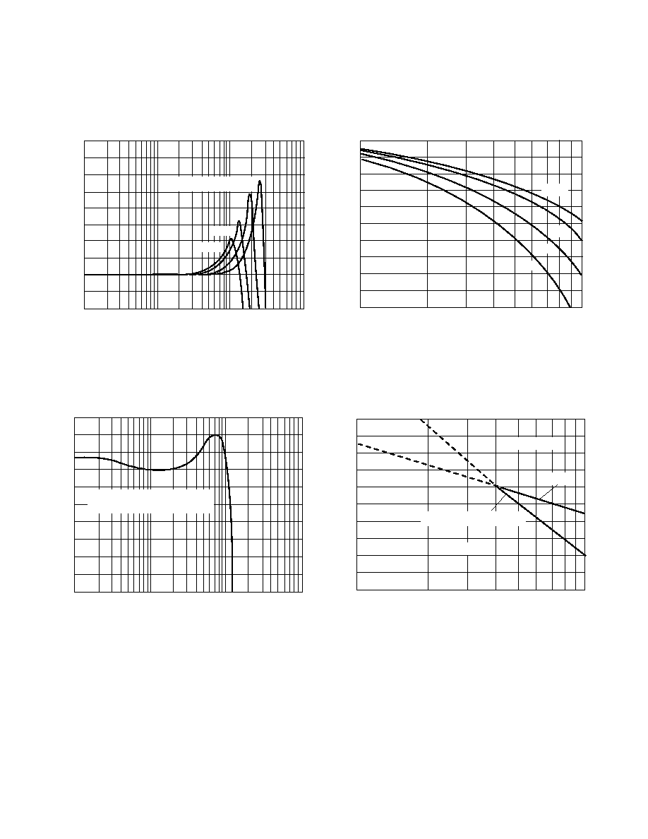
Fig. 1 Gain vs Frequency
Fig. 2 Phase vs Frequency
Load Capacitance
22 pF
10 pF
47 pF
82 pF
22 pF
47 pF
82 pF
10 pF
TYPICAL PERFORMANCE CURVES OF THE GX4201
For all graphs, V
S
=
±
5 V DC and T
A
= 25
∞
C. The curves shown below represent typical batch sampled results.
Gain (dB)
0.1
0.05
0
-0.05
-0.1
-0.15
-0.2
-0.25
-0.3
-0.35
-0.4
1
10
100
1K
Fig. 3 Gain vs Frequency
Frequency (MHz)
Frequency (MHz)
10
20
30
50
80 100
Fig. 4 Off Isolation vs Frequency
Off
Isolation (dB)
External Series Resistance = 30
C
L
= 33 pF
continued over
R
L
= 10
V
IN
= 1V p-p
(See test circuits)
120
110
100
90
80
70
Load = 1 xpt on O/P to GND
3

510 - 74 - 5
1
5
6
8
4
3
2
7
0.1
-5 V
+5 V
OUTPUT
0.1
2 x BFR96
180
180
0.1
-5 V
INPUT
10
I
L
ADJUST FOR
= 6mA
I
L
LOAD
1K
1
5
6
8
4
3
2
7
0.1
-5 V
+5 V
1
5
6
8
4
3
2
7
OUTPUT
0.1
0.1
0.1
ON DEVICE
OFF DEVICE
2 x BFR96
180
180
0.1
-5 V
INPUT
I
L
ADJUST FOR
= 6mA
I
L
1K
10
10
+
+
-5 V
+5 V
V
CTRL
6mA
-5 V
10pF
V
OUT
74LS02
1
5
6
8
4
3
2
7
1
5
6
8
4
3
2
7
All capacitors in farads, all resistors in ohms unless otherwise stated.
Fig. 11a Switching Transient Test Circuit
Fig. 11b Switching Transient
Active Load
Passive Load
Fig. 12 Off-isolation Test Circuits
NOTE: Off-isolation can be increased by eliminating the signal path
through the power supplies. This is demonstrated by replacing the
enabled crosspoint with a 10
load resistor as shown in the passive
load circuit.
Fig. 10 Burn-in Test Circuit
10 mV/div
200 mV/div
1
µ
s/div
V
CRTL
V
OUT
1
5
6
8
4
3
2
7
5.5 K
470
10
10
+
+
-5.5 V
+5.5 V
5

