GENNUM CORPORATION P.O. Box 489, Stn. A, Burlington, Ontario, Canada L7R 3Y3
Tel. +1 (905) 632-2996 Fax. +1 (905) 632-5946 E-mail: info@gennum.com
www.gennum.com
Revision Date: August 1999
Document No. 521 - 41 - 03
DATA SHEET
G
X
9
533
FEATURES
∑ operation beyond 622Mb/s
∑ accepts SMPTE and PECL input levels
∑ fully differential signal path
∑ on-chip PECL current loads eliminate need for
external pull-down resistors
∑ capable of driving 100
differential loads
∑ very low 500mW power consumption
∑ additional expansion port input for construction of
larger matrices
∑ auxiliary monitoring output
∑ easy to configure
∑ double latched address inputs with separate load and
configure
∑ TTL/CMOS compatible control logic inputs
∑ single 5V power supply
APPLICATIONS
Serial digital video switching; datacom or telecom
switching.
DESCRIPTION
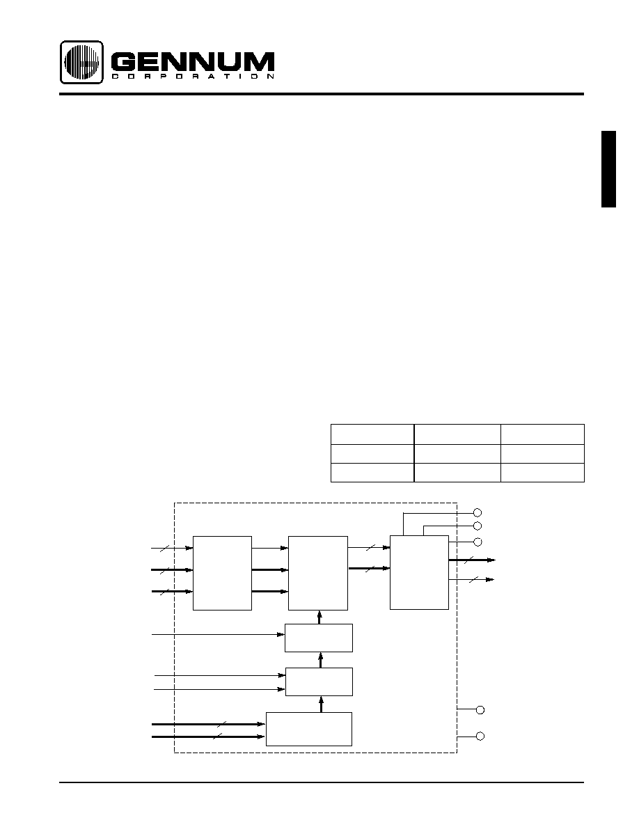
The GX9533 is a high speed 8x9 serial digital crosspoint.
An expansion input port eases the design of larger
switching matrices by reducing PCB layers and eliminating
the need for cascaded secondary switching. Decode logic
and double level latching to configure the matrix are
included on chip. Separate LOAD and CONFIGURE inputs
allow for asynchronous configuration and synchronous
switching. These latches can also be made transparent for
asynchronous switching by pulling the LOAD and
CONFIGURE pins high.
In the power saving (PS) mode, the GX9533 has a very low
power consumption of 500mW. This is accomplished by
driving a 400mV output swing into the on-chip 200
differential load termination in the expansion port of the next
GX9533. This architecture provides a significant power
savings and the elimination of external load resistors or
impedance matching resistors. In applications where
standard PECL levels are necessary, the GX9533 can be
configured in "PECL Mode", to drive 800mV p-p into a 100
differential load. The power consumption in this mode
increases to 860mW.
BLOCK DIAGRAM
ORDERING INFORMATION
PART NUMBER
PACKAGE
TEMPERATURE
GX9533-CQY
100 pin MQFP Tray
0∞C to 70∞C
GX9533-CTY
100 pin MQFP Tape
0∞C to 70∞C
IN0 .. 7
EXP0..7
AUX IN
OA0..2
IA0..3
V
CC
AUX
V
EE
V
CCO
STD/PECL1
STD/PECL2
CONFIG
LOAD A
LOAD
CONFIG
LATCH
LOAD
LATCH
16
16
16
16
3
4
2
2
2
OUT 0..7
DECODE
LOGIC
SWITCHING
MATRIX
INPUT
BUFFER
OUTPUT
BUFFER
GENLINX
TM
II
GX9533
Serial Digital 8x9 Crosspoint

521 - 41 - 03
2
G
X
953
3
ABSOLUTE MAXIMUM RATINGS
PARAMETER
VALUE
Supply Voltage (V
S
= V
CC
-V
EE
)
5.5V
Input Voltage Range (any input)
-0.3 to (V
CC
+0.3)V
Power Dissipation
975mW
Operating Temperature Range
0∞C to 70∞C
Storage Temperature Range
-65∞C to +150∞C
Lead Temperature Range (soldering, 10 sec)
260∞C
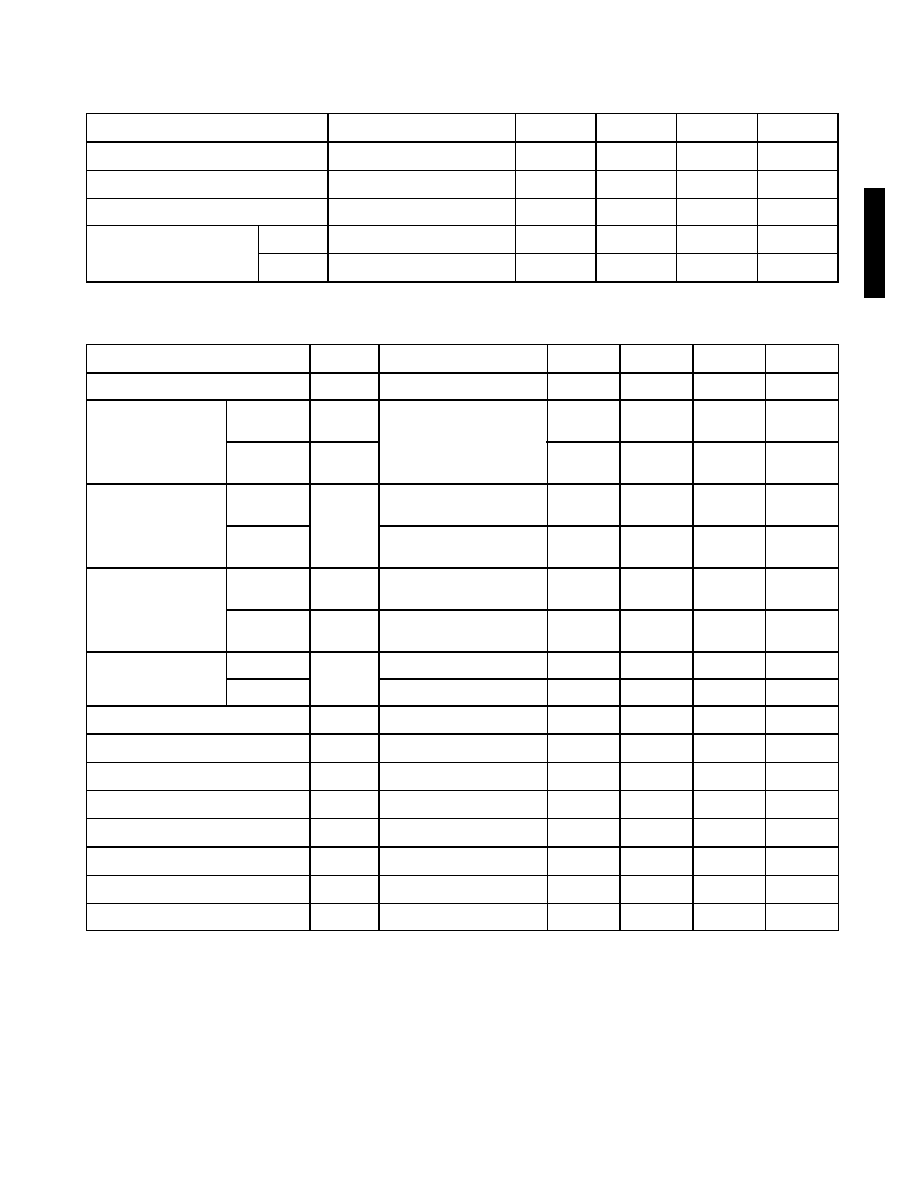
DC ELECTRICAL CHARACTERISTICS
V
CC
= 5V, V
EE
= 0V, T
A
= 0 to 70∞C unless otherwise shown.
PARAMETER
CONDITION
MIN
TYP
MAX
UNITS
Supply Voltage
4.75
5.0
5.25
V
ECL Input Voltage Swing
200
800
1200
mV p-p
ECL Common Mode Input Voltage Range
with 1200mV input signal swing
2500
-
V
CC
-600
mV
Logic Input Voltage
High
2.0
-
V
CC
V
Low
0
-
0.8
V
POWER SAVE 1 MODE
R
SET
= 4k
PARAMETER
CONDITION
MIN
TYP
MAX
UNITS
Supply Current
R
L
= 100
-
115
150
mA
Output Common Mode Voltage
V
CC
-1200
-
V
CC
-800
mV
Output Voltage Swing
300
450
600
mV
Output Voltage
High
V
CC
-950
-
V
CC
-600
mV
Low
V
CC
-1400
-
V
CC
-1000
mV
POWER SAVE 2 MODE
R
SET
= 6k
PARAMETER
CONDITION
MIN
TYP
MAX
UNITS
Supply Current
R
L
= 200
-
100
130
mA
Output Common Mode Voltage
V
CC
-1200
-
V
CC
-800
mV
Output Voltage Swing
300
450
600
mV
Output Voltage
High
V
CC
-950
-
V
CC
-600
mV
Low
V
CC
-1400
-
V
CC
-1000
mV
521 - 41 - 03
3
G
X
9
533
PECL MODE
R
SET
= 2k
PARAMETER
CONDITION
MIN
TYP
MAX
UNITS
Supply Current
R
L
= 100
-
170
185
mA
Output Common Mode Voltage
V
CC
-1450
-
V
CC
-1050
mV
Output Voltage Swing
700
800
900
mV
Output Voltage
High
V
CC
-1200
-
V
CC
-650
mV
Low
V
CC
-1850
-
V
CC
-1450
mV
AC ELECTRICAL CHARACTERISTICS
V
CC
= 5.0V, V
EE
= 0V, T
A
= 0 to 70∞C unless otherwise shown.
PARAMETER
SYMBOL
CONDITION
MIN
TYP
MAX
UNITS
Maximum Input Data Rate
For 90% eye opening
-
850
-
Mb/s
Additive Jitter
Standard
Input
143 to 622 Mb/s, all hostile
crosstalk
-
80
-
ps p-p
Expansion
Input
-
70
-
ps p-p
Data In to Data Out
Delay
Standard
Input
t
DLY
Average of all channels
-
1.7
-
ns
Expansion
Input
-
1.1
-
ns
Propagation Delay
Match
Standard
Input
-
350
-
ps
Expansion
Input
-
250
-
ps
CONFIGURE to Data
Out Delay
Main Out
t
CD
-
10
-
ns
AUX Out
-
11
-
ns
LOAD/LOADA Pulse Width
t
LP
20
-
-
ns
CONFIGURE Pulse Width
t
CP
20
-
-
ns
IA
N
to LOAD/LOADA High Setup Time
t
ILS
30
-
-
ns
LOAD/LOADA to IA
N
Low Hold Time
t
ILH
0
-
-
ns
OA
N
to LOAD High Setup Time
t
OLS
30
-
-
ns
LOAD to OA
N
Low Hold Time
t
OLH
0
-
-
ns
LOAD High to CONFIGURE High
t
LC
0
-
-
ns
Output Rise/Fall Time
-
700
-
ps
NOTE
1. Use RMS addition to calculate additive jitter through cascaded devices.
521 - 41 - 03
4
G
X
953
3
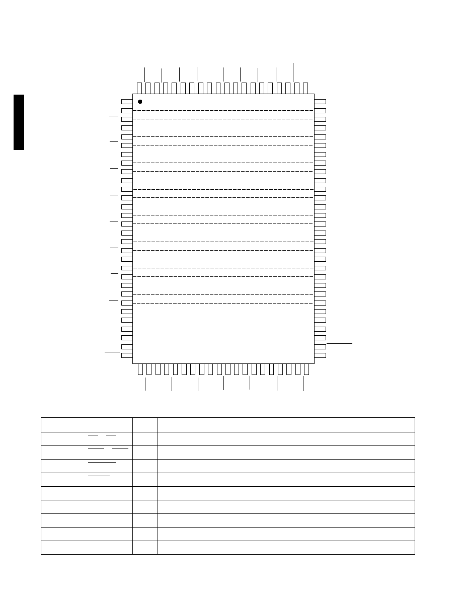
PIN CONNECTIONS
PIN DESCRIPTIONS
SYMBOL
TYPE
DESCRIPTION
IN0 to IN7, IN0 to IN7
I
Differential data inputs.
OUT0 to OUT7, OUT0 to OUT7
O
Differential data outputs.
AUX_OUT, AUX_OUT
O
Auxiliary port output.
AUX_IN, AUX_IN
I
Auxiliary port input.
OA0 to OA2
I
Output address select.
IA0 to IA3
I
Input address select.
LOAD
I
Loads input & output address.
LOADA
I
Loads auxiliary input address.
STD/ECL1, STD/ECL2
Resistor connection for Power Save mode or PECL mode. Refer to Table 3.
STD/PECL1
NC
NC
LOAD
NC
NC
LOADA
NC
NC
CNFG
NC
NC
IA0
NC
NC
IA1
NC
NC
IA2
NC
NC
IA3
NC
NC
OA0
OA1
OA2
V
EE
AUX_OUT
AUX_OUT
V
CC
IN0
IN0
V
EE
IN1
IN1
V
EE
IN2
IN2
V
EE
IN3
IN3
V
EE
IN4
IN4
V
EE
IN5
IN5
V
EE
IN6
IN6
V
EE
IN7
IN7
V
EE
V
EE
V
CC
V
EE
OUT0
OUT0
OUT1
OUT1
V
CCO
OUT2
OUT2
V
CCO
OUT3
OUT3
V
CCO
OUT4
OUT4
V
CCO
OUT5
OUT5
V
CCO
OUT6
OUT6
V
CCO
OUT7
OUT7
EXP0
EXP0
EXP1
EXP1
EXP2
EXP2
EXP3
EXP3
V
CC
EXP4
EXP4
EXP5
EXP5
EXP6
EXP6
EXP7
EXP7
AUX_IN
AUX_IN
STD/PECL2
GX9533
TOP VIEW

521 - 41 - 03
5
G
X
9
533
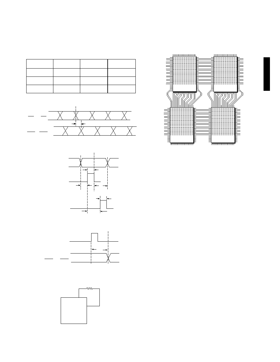
Fig. 1 Data Flow Diagram
Fig. 2 Typical Eye Opening vs. Bit Rate
CNFG
I
Switch configuration.
EXP0 to EXP7, EXP0 to EXP7
I
Expansion port inputs.
V
CC
Positive power supply.
V
CCO
Positive power supply (PECL outputs).
V
EE
Negative power supply.
PIN DESCRIPTIONS
SYMBOL
TYPE
DESCRIPTION
Standard
Inputs
Auxilliar
y
Input
Auxilliar
y
Output
Main
Outputs
0
1
2
3
4
5
6
7
8
INPUT B
UFFERS
0
1
2
3
4
5
7
6
Expansion
Inputs
0
1
2
3
4
5
7
6
4x1
Switch
3x1
Switch
4x1
Switch
4
5
6
7
0
1
2
3
4x1
Switch
4
5
7
6
0
1
2
3
4x1
Switch
3x1
Switch
700 800 900 1000 1100
100
90
80
70
60
50
BIT RATE (Mb/s)
% OPENING
521 - 41 - 03
6
G
X
953
3
DETAILED DESCRIPTION
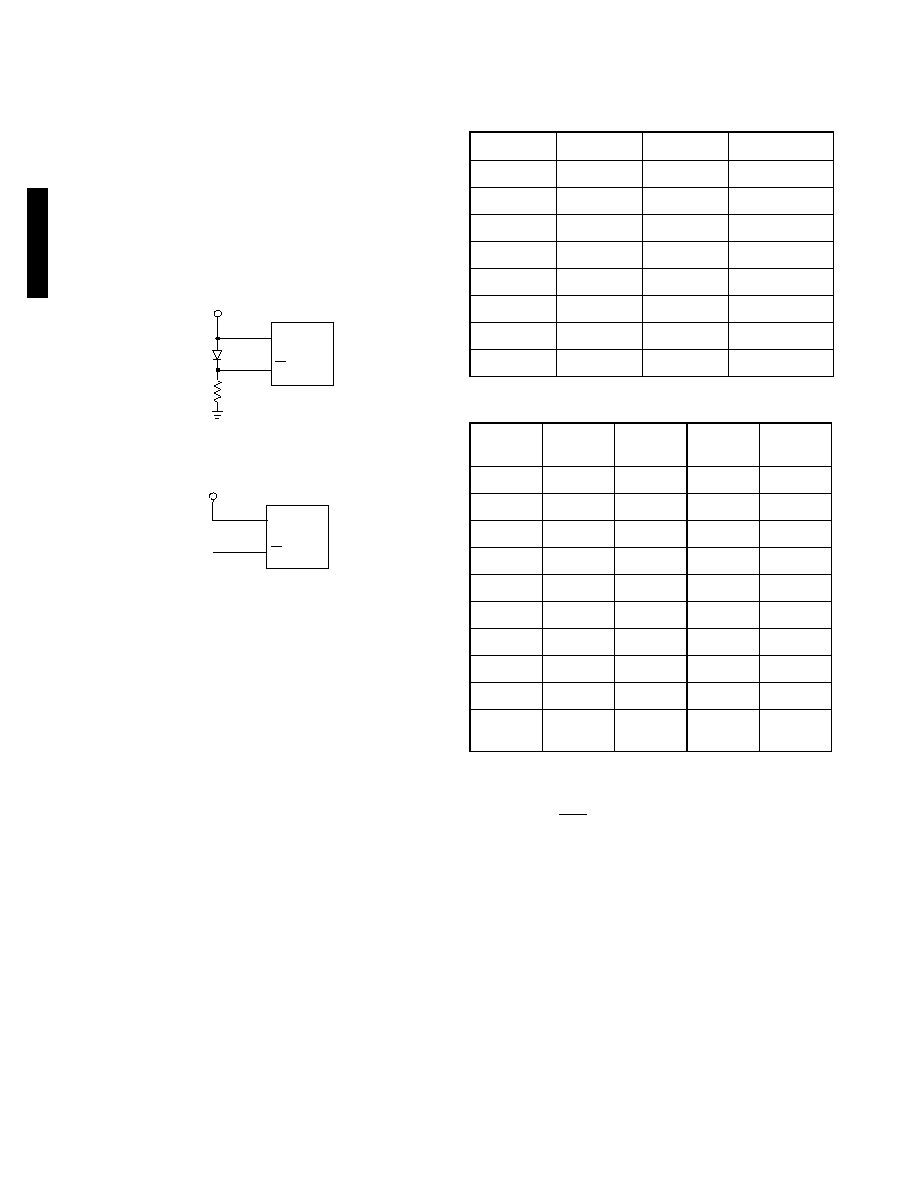
DIFFERENTIAL INPUTS
The inputs to the GX9533 will accept both SMPTE 259M as
well as PECL input levels. The fully differential data path
provides low jitter data rates of up to 700Mb/s.
The main inputs (IN0..7) and expansion inputs (EXP0..7) are
normally connected to a biased differential data source.
The GX9533 inputs are not self biased, so unused inputs
should be connected as shown in Figure 3 or Figure 4.
Fig. 3 Preferred Termination Of Unused Inputs
Fig. 4 Alternate Termination of Unused Inputs
Terminating the inputs as shown in Figure 3 will provide the
highest noise immunity, since there is no possibility of noise
coupling into the unconnected input pin.
I/O ADDRESS SELECTION
The GX9533 has a versatile LOAD/CONFIGURE
architecture which simplifies IN/OUT switch configuration.
An output is normally connected to an input by a two stage
process:
Stage One: Loading The Configuration Into Latches
1. The output address is selected on the OA pins as
shown in Table 1.
2. The input address is selected on the IA pins as shown in
Table 2.
3. A LOAD pulse then transfers the output and input
addresses into the GX9533 LOAD latch.
The above three steps can be repeated up to eight times in
order to configure the latch for all eight outputs.
During step 3 above, if the LOADA pulse is also strobed,
the latch is configured to connect the selected input to the
ninth, auxiliary output.
Note that a QUIET mode is available as shown in Table 2. In
QUIET mode, the outputs are latched in a DC state with
OUT
X
= 1 and OUT
X
= 0.
Stage Two: Configuring The Matrix
A CONFIGURE strobe is applied to transfer the contents of
the LOAD latch into the CONFIG latch. This action will
cause the data flow through the GX9533 to be switched to
the new configuration. Refer to Figure 6 for detailed timing
information.
Note that any single output can be asynchronously
switched by having LOAD (or LOADA if desired) held high
while CONFIG is strobed.
IN
x
IN
x
GX9533
V
CC
1k
IN
X
IN
X
GX9533
V
CC
NC
TABLE 1: Output Address Selection
OA2
0A1
0A0
OUTPUT PORT
0
0
0
0
0
0
1
1
0
1
0
2
0
1
1
3
1
0
0
4
1
0
1
5
1
1
0
6
1
1
1
7
TABLE 2: Input Source Address Selection
IA3
IA2
IA1
IA0
INPUT
PORT
0
0
0
0
0
0
0
0
1
1
0
0
1
0
2
0
0
1
1
3
0
1
0
0
4
0
1
0
1
5
0
1
1
0
6
0
1
1
1
7
1
0
X
X
EXP
1
1
X
X
Quiet
Mode
521 - 41 - 03
7
G
X
9
533
OUTPUT LEVEL SELECT
A single resistor, R
SET
, is used to set the amplitude of all
differential outputs. Table 3 shows the value of R
SET
vs
output drive capability.
Fig. 5 GX9533 Data Latency
Fig. 6 LOAD/LOADA and Configure Timing
Fig. 7 Configure to Data Out Delay
Fig. 8 GX9533 R
SET
Connection
USING THE GX9533 TO EXPAND LARGER MATRICES
The GX9533 pin-out and architecture provides a number of
advantages over other crosspoint switches in the area of
switching matrix board layout.
Fig. 9 Crosspoint Matrix Expansion - 16x16 Crosspoint Matrix
BUS THROUGHTM PIN CONNECTIONS
To easily facilitate a switching matrix design where inputs
can be bussed across a matrix of crosspoint devices,
Gennum's crosspoint device has "NC" pins opposite the
input pins as shown by the dotted lines in the pin-out
diagram above. This design allows bussing of inputs
without having to use "vias" to get below the top layer of the
printed circuit board.
EXPANSION PORT INPUT
The expansion inputs provide the following benefits:
∑
by not having to run traces from the outputs of the
crosspoint switch to a common output bus, crosstalk
between output channels can be greatly reduced.
∑
fewer circuit board layers are required because the
outputs of each device simply line up
∑
there are no transmission line effects caused by
connecting High-Z outputs to an output bus
∑
because the output signal is being routed from the top
of the switching matrix to the bottom through the
devices, inputs can be simply bussed across the board
without having to worry about input/output crosstalk.
TABLE 3: R
SET
vs V
OUT
R
SET
V
OUT
(mV)
OUTPUT R
L
MODE
2k
800
100
PECL
4k
450
100
Power Save 1
6k
450
200
Power Save 2
IN0 to IN7
IN0 to IN7
OUT0 to OUT7
OUT0 to OUT7
t
DLY
OA
N
, IA
N
t
ILS
t
OLS
t
LP
t
ILH
t
OCH
t
LC
t
CP
LOAD/LOADA
CONFIGURE
CONFIGURE
t
CD
OUT 0 TO OUT 7
OUT 0 TO OUT 7
R
SET
STD/ECL2
STD/ECL1
GX9533
INPUTS 8-15
INPUTS 0-7
OUTPUTS 8-15
OUTPUTS 0-7
GX9533
GX9533
GX9533
GX9533
521 - 41 - 03
8
GENNUM CORPORATION
MAILING ADDRESS:
P.O. Box 489, Stn. A, Burlington, Ontario, Canada L7R 3Y3
Tel. +1 (905) 632-2996 Fax. +1 (905) 632-5946
SHIPPING ADDRESS:
970 Fraser Drive, Burlington, Ontario, Canada L7L 5P5
GENNUM JAPAN CORPORATION
C-101, Miyamae Village, 2-10-42 Miyamae, Suginami-ku
Tokyo 168-0081, Japan
Tel. +81 (03) 3334-7700 Fax. +81 (03) 3247-8839
GENNUM UK LIMITED
Centaur House, Ancells Bus. Park, Ancells Rd, Fleet, Hants, England GU13 8UJ
Tel. +44 (0)1252 761 039 Fax +44 (0)1252 761 114
Gennum Corporation assumes no responsibility for the use of any circuits described herein and makes no representations that they are free from patent infringement.
© Copyright April 1995 Gennum Corporation. All rights reserved. Printed in Canada.
G
X
953
3
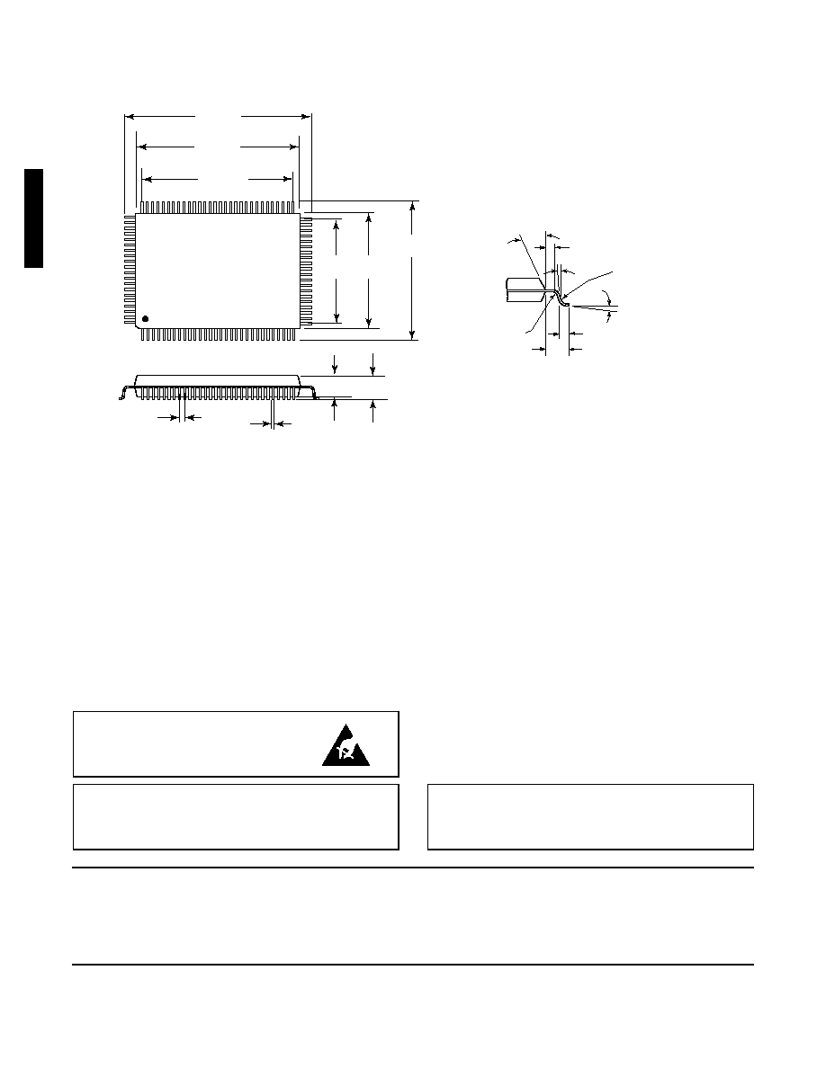
PACKAGE DIMENSIONS
23.90
±0.25
20.0
±0.10
18.85
REF
17.90
±0.25
14.0
±0.10
12.35
REF
3.30 MAX
2.80
±0.25
1.95
REF
0.30 MAX RADIUS
0.13 MIN.
RADIUS
0.80
±0.10
0.75 MIN
12∞ TYP
0∞- 7∞
0∞-7∞
0.30
±0.08
0.65
BSC
100 pin MQFP
Dimensions in millimeters
REVISION NOTES:
Changes to document format.
DOCUMENT IDENTIFICATION
DATA SHEET
The product is in production. Gennum reserves the right to make
changes at any time to improve reliability, function or design, in order to
provide the best product possible.
CAUTION
ELECTROSTATIC
SENSITIVE DEVICES
DO NOT OPEN PACKAGES OR HANDLE
EXCEPT AT A STATIC-FREE WORKSTATION