NOT RECOMMENDED
FOR NEW DESIGNS
8.2 k
Q1
GND
3
Q2
Q3
O/P
2
3.5 k
1
V
B
I/P
4
LC507 DATA SHEET
DESCRIPTION
The LC507 is a low voltage, 3 stage, linear class A amplifier,
available in a Gennum single-in-line 4 pin MICROpac. The
LC507 features high gain, low current and a wide frequency
response.
The simplicity of the design allows the LC507 to be used with
a minimal amount of external components to produce low
voltage miniature electronic devices.
The electrical and packaging specifications make the LC507
suitable as a pin for pin replacement for three transitor amplifiers
such as the Philips OM 200 and Siemens TAA 141 .
FEATURES
∑ 76 dB typical gain (open loop)
∑ 1.0 to 3 VDC operating range
∑ frequency response 20 kHz (min)
∑ Total harmonic distortion 2%
STANDARD PACKAGING
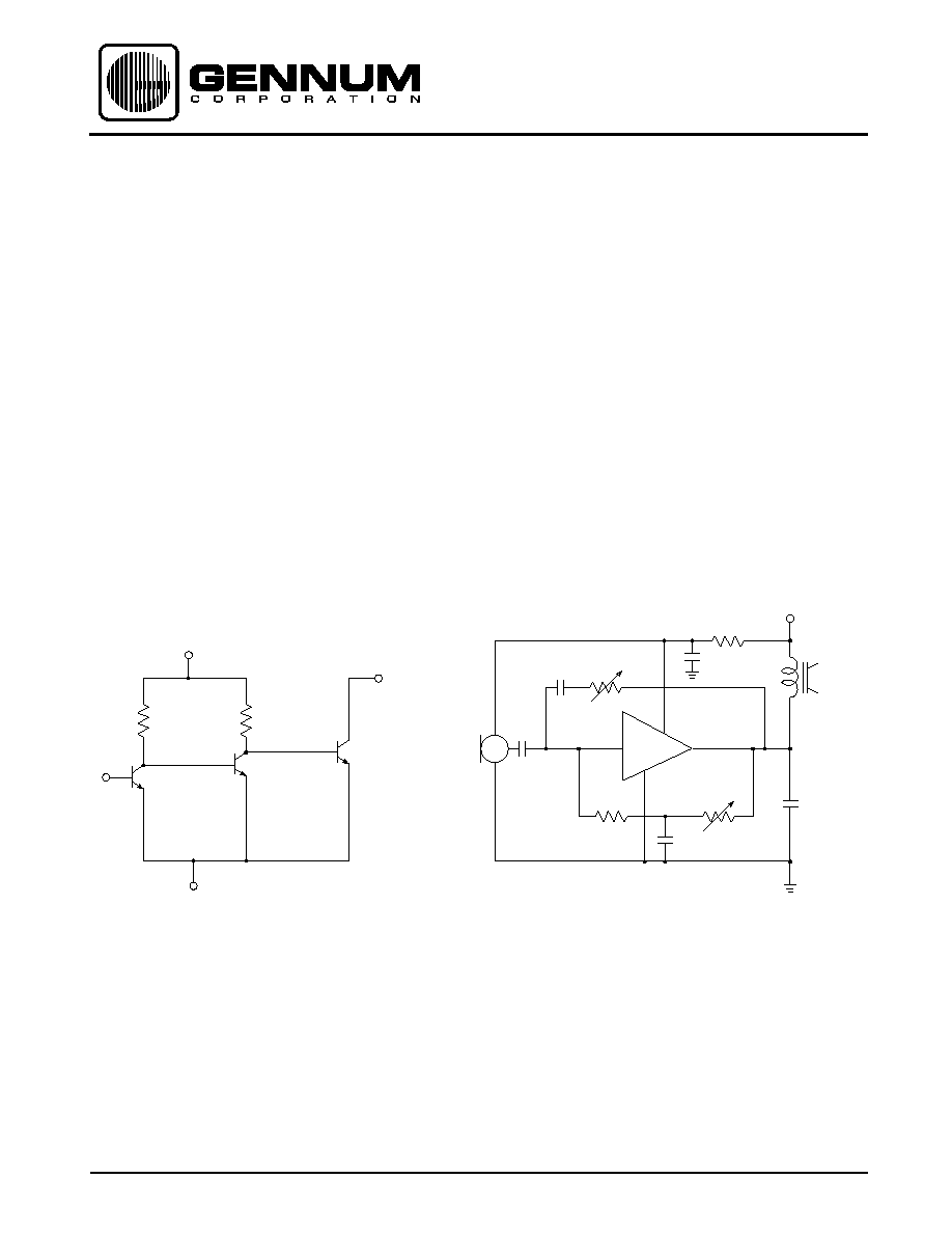
TYPICAL HEARING AID CIRCUIT
FUNCTIONAL SCHEMATIC
High Gain Class A Amplifier
Revision Date: June 1998
LC507
0.1
1.0
4.7 M
10
+
1 k
V
B
= 1.35 VDC
R
L
= 1.5k
0.1
I
TRIM
1 M
1.0
4.7k
1
2
3
4
V
C
R
S
= 3.9k
All resistors in ohms, all capacitors in microfarads unless otherwise stated
∑
4 pin MICROpac
∑
8 pin PLID
Document No. 500 - 46 - 10
GENNUM CORPORATION P.O. Box 489, Stn A, Burlington, Ontario, Canada L7R 3Y3 tel. (905) 632-2996 fax: (905) 632-2814
Gennum Japan Corporation: C-101, Miyamae Village, 2-10-42 Miyamae, Suginami-ku, Tokyo 168-0081, Japan tel. (03) 3334-7700 fax:(03) 3247-8839

2
500 - 46 - 10
NOT RECOMMENDED
FOR NEW DESIGNS
1
4
PIN CONNECTION
(In MICROpac pins 1
to 4 do not exist)
ABSOLUTE MAXIMUM RATINGS
PARAMETER SYMBOL CONDITIONS
MIN TYP MAX UNITS
Voltage Gain (closed loop) A
CL
Output Level= 0.2 mW
Total Harmonic Distortion THD
Output Level= 0.2 mW
Total Current
I
TOTAL
Frequency Response at -3 dB
High
Low
Potentiometer Resistance
I
L
= 0.7 mA
56
-
-
-
-
40
ELECTRICAL CHARACTERISTICS
Conditions: Supply Voltage 1.3 VDC, Transducer current
I
L
= 0.7 mA, Ambient temperature 25∞C
58
2.0
1.0
20
0.2
500
dB
%
mA
kHz
kHz
k
60
3.5
1.2
-
-
1000
PARAMETER
VALUE / UNITS
Supply Voltage
5 VDC
Power Dissipation 25 mW
Storage Temperature -20 to + 80∞C
Operating Temperature
-20 to + 80∞C
CAUTION
CLASS 1 ESD SENSITIVITY
Gennum Corporation assumes no responsibility for the use of any circuits described herein and makes no representations that they are free from patent infringement.
© Copyright September 1982 Gennum Corporation. All rights reserved. Printed in Canada.
5
8
LC507
1
2
3
4
9k
47k
470
4.7 M
0.022
1:1
99966
1K
R2
0.022
1M
R
F
4.7k
R
S
1.0
100
1kHz
490
R1
1.0
V
IN
V
B
= 1.3VDC
V
OUT
I
L
1.0
All external resistors in ohms, all capacitors in microfarads unless otherwise stated
Fig. 1 Test Circuit
I/P
GND
O/P
V
B
N/C
N/C
N/C
N/C
DOCUMENT IDENTIFICATION
PRODUCT PROPOSAL
This data has been compiled for market investigation purposes
only, and does not constitute an offer for sale.
ADVANCE INFORMATION NOTE
The product is in a development phase and specifications are
subject to change without notice. Gennum reserves the right to
remove the product at any time. Listing the product does not
constitute an offer for sale.
PRELIMINARY DATA SHEET
The product is in a preproduction phase and specifications are
subject to change without notice.
DATA SHEET
The product is in production. Gennum reserves the right to make
changes at any time to improve reliability, function or design, in
order to provide the best product possible.
REVISION NOTES
Packaging information correction