G -LINK
GLT6100L08
Ultra Low Power 128k x 8 CMOS SRAM
Nov 2000(Rev. 02)
G-Link Technology Corporation
2701 Northwestern Parkway
Santa Clara, CA 95051, U.S.A.
G-Link Technology Corporation, Taiwan
6F No. 24-2, Industry E. RD. IV, Science Based
Industrial Park, Hsin Chu, Taiwan.
- 1 -
Features :
Description :
Low-power consumption.
-active: 30mA at 55ns.
-Stand by :
5
µ
A (CMOS input / output)
1
µ
A (CMOS input / output, SL)
Single +2.7 to 3.3V Power Supply.
Equal access and cycle time.
55/70/85/100 ns access time.
Easy memory expansion with
CE1
,
CE2 and
OE
inputs.
2.0V data retention mode.
TTL compatible, Tri-state input/output.
Automatic power-down when
deselected.
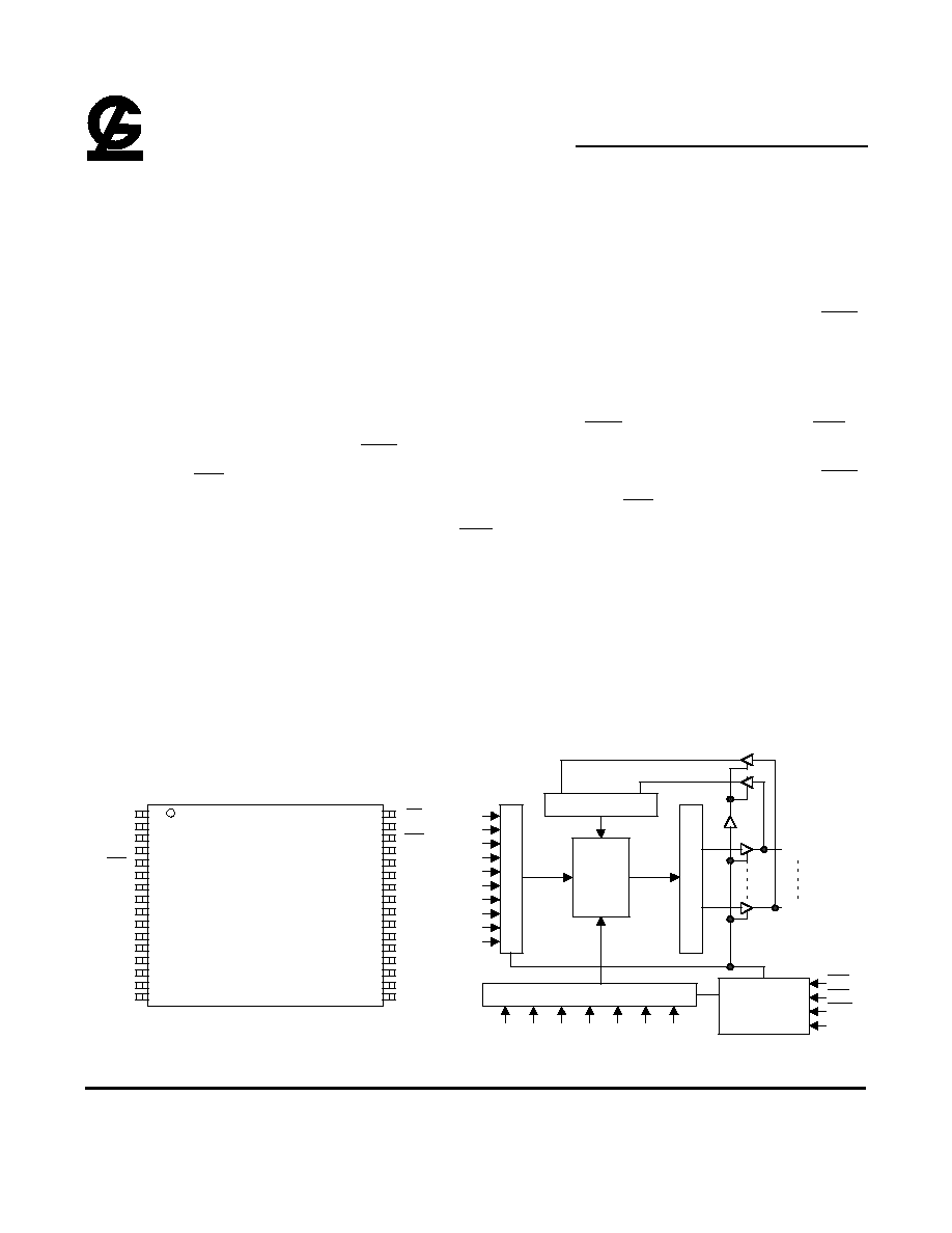
The GLT6100L08 is a low power CMOS Static
RAM organized as 131,072 words by 8 bits. Easy
memory expansion is provided by an active LOW
CE1
, an active HIGH CE2, an active LOW OE, and Tri-
state I/O's. This device has an automatic power-
down mode feature when deselected.
Writing to the device is accomplished by taking
chip Enable 1 (
CE1
) with Write Enable (
WE
)
LOW, and Chip Enable 2 (CE2) HIGH. Reading from
the device is performed by taking Chip Enable 1 (
CE1
) with Output Enable (
OE
) LOW while Write Enable
(
WE
) AND Chip Enable 2 (CE2) is HIGH. The I/O
pins are placed in a high-impedance state when the
device is deselected : the outputs are disabled during
a write cycle.
The GLT6100L08 comes with a 2V data retention
feature and Lower Standby Power. The GLT6100L08
is available in a 32-pin TSOPI / sTSOP / 48-fpBGA
packages.
Pin Configurations :
GLT6100L08
A
16
A
7
1
2
3
4
5
6
8
9
10
11
12
13
22
21
19
18
17
26
25
24
23
GND
OE
A
10
14
27
28
I/O
8
I/O
7
20
A
0
7
WE
V
CC
NC
15
16
29
30
31
32
A
11
A
9
A
8
A
13
CE
2
A
15
A
14
A
12
A
6
A
5
A
4
A
3
A
2
A1
I/O
1
I/O
2
I/O
3
I/O
4
I/O
5
I/O
6
CE
1
Function Block Diagram :
ROW DECODER
1024
x
1024
SENSE AMP
INPUT BUFFER
COLUMN DECODER
A
10
A
11
A
12
A
13
A
14
A
15
A
16
A
0
A
1
A
2
A
3
A
4
A
5
A
6
A
7
A
8
A
9
CONTROL
CIRCUIT
OE
WE
CE1
CE2
I/O
8
I/O
1
G -LINK
GLT6100L08
Ultra Low Power 128k x 8 CMOS SRAM
Nov 2000(Rev. 02)
G-Link Technology Corporation
2701 Northwestern Parkway
Santa Clara, CA 95051, U.S.A.
G-Link Technology Corporation, Taiwan
6F No. 24-2, Industry E. RD. IV, Science Based
Industrial Park, Hsin Chu, Taiwan.
- 2 -
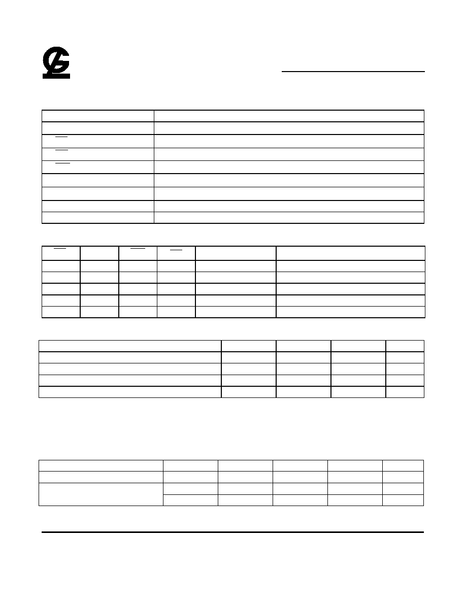
Pin Descriptions:
Name
Function
A - A
0
16
Address Inputs
CE
1
and CE
2
Chip Enable Input
OE
Output Enable Input
WE
Write Enable Input
I O
I O
0
7
/
/
-
Data Input and Data Output
V
CC
3V Power Supply
GND
Ground
NC
No Connection
Truth Table:
CE
1
CE
2
WE
OE
Data
Mode
H
X
X
X
High-Z
Standby
X
L
X
X
High-Z
Standby
L
H
H
L
Data Out
Active, Read
L
H
H
H
High-Z
Active, Output Disable
L
H
L
X
Data Out
Active, Write
Absolute Maximum Ratings*
Parameter
Symbol
Minimum
Maximum
Unit
Voltage on Any Pin Relative to Gnd
Vt
-0.5
4.6
V
Power Dissipation
P
T
-
1.0
W
Storage Temperature (Plastic)
Tstg
-55
+150
∞
C
Temperature Under Bias
Tbias
-40
+85
∞
C
*Note : Stresses greater than those listed above Absolute Maximum Ratings may cause permanent damage to the device.
This is a stress rating only and functional operation of the device at these or any conditions outside those indicated
in the operational sections of this specification is not implied. Exposure to absolute maximum rating conditions for
extended periods may affect reliability.
Recommended Operating Conditions ( TA = -25
∞
C to 85
∞
C )**
Parameter
Symbol
Min
Typ
Max
Unit
Supply Voltage
V
CC
2.7
3.0
3.3
V
V
IH
2.2
-
V
CC
+0.5
V
Input Voltage
V
IL
-0.5*
-
0.6
V
* V
IL
min = -1.0V for pulse width less than t
RC
/2.
** For Industrial Temperature.

G -LINK
GLT6100L08
Ultra Low Power 128k x 8 CMOS SRAM
Nov 2000(Rev. 02)
G-Link Technology Corporation
2701 Northwestern Parkway
Santa Clara, CA 95051, U.S.A.
G-Link Technology Corporation, Taiwan
6F No. 24-2, Industry E. RD. IV, Science Based
Industrial Park, Hsin Chu, Taiwan.
- 3 -
DC Operating Characteristics
( Vcc=2.7V to 3.3V, T
A
=-25
∞
C to 85
∞
C )
55
70
85
100
Parameter
Sym.
Test Conditions
Min Max Min Max Min Max Min Max
Unit
Input Leakage Current
I
LI
V
CC
= Max,
Vin = Gnd to V
CC
1
1
1
1
µ
A
Output Leakage
Current
I
LO
CE
1
=V
IH
or CE2 = V
IH
V
CC
= Max, V
OUT
= Gnd to V
CC
1
1
1
1
µ
A
Operating Power
Supply Current
I
CC
CE
1
=V
IL
,CE2 = V
IH
V
IN
=V
IH
or V
IL
, I
OUT
=0mA
3
3
3
3
mA
I
CC1
CE
1
=V
IL
,CE2 = V
IH
I
OUT
= 0mA,
Min Cycle, 100% Duty
30
25
20
15
mA
Average Operating
Current
I
CC2
CE
1
=0.2V
CE2 = V
CC
≠ 0.2V
I
OUT
= 0mA,
Cycle Time=1
µ
s, 100% Duty
3
3
3
3
mA
Standby Power Supply
Current(TTL Level)
I
SB
CE
1
=V
IH
or CE2 = V
IL
0.5
0.5
0.5
0.5
mA
GLT6100L08LL
5
5
5
5
µ
A
Standby Power Supply
Current (CMOS Level)
I
SB1
CE
1
V
CC
-
0.2V or
CE2
0.2V, f=0
V
IN
0.2V or
V
IN
V
CC
-0.2V
GLT6100L08SL
1
1
1
1
µ
A
Output Low Voltage
V
OL
I
OL
= 2 mA
0.4
0.4
0.4
0.4
V
Output High Voltage
V
OH
I
OH
= 2 mA
2.4
2.4
2.4
2.4
V
Data Retention
Parameter
Sym.
Test Conditions
Min.
Max.
Unit
V
CC
for Data retention
V
DR
1.0
-
V
Data Retention Current
I
CCDR
5
µ
A
Chip Deselect to Data Retention Time
t
CDR
0
-
ns
Operating Recovery Time
(2)
t
R
CE
1
V
CC
-0.2V or
CE
2
+0.2V,
V
IN
V
CC
-0.2V or
V
IN
0.2V
t
RC
-
ns

G -LINK
GLT6100L08
Ultra Low Power 128k x 8 CMOS SRAM
Nov 2000(Rev. 02)
G-Link Technology Corporation
2701 Northwestern Parkway
Santa Clara, CA 95051, U.S.A.
G-Link Technology Corporation, Taiwan
6F No. 24-2, Industry E. RD. IV, Science Based
Industrial Park, Hsin Chu, Taiwan.
- 4 -
Data Retention Waveform
(TA = -25
∞
C to 85
∞
C)
Data Retention Mode
Vcc
CE
V
DR
V
DR >= 1.0V
t
R
t
CDR
2.7V
2.7V
V
IH
V
IH
AC Test Conditions
AC Test Loads and Waveforms
C
L
*
TTL
Output Load Condition
*Including Scope and Jig Capacitance
70ns / 85ns
C
L
= 30pf + 1TTL Load
Load 100ns / 120ns
C
L
= 100pf + 1TTL Load
Read Cycle
(3,9)
( Vcc=2.7V to 3.3V, T
A
=-25
∞
C to 85
∞
C )
55
70
85
100
Parameter
Symbol
Min Max Min Max Min Max Min Max
Unit Note
Read Cycle Time
t
RC
55
70
85
100
ns
Address Access Time
t
AA
55
70
85
100
ns
Chip Enable Access Time
t
ACE
55
70
85
100
ns
Output Enable Access Time
t
OE
35
40
40
50
ns
Output Hold from address Change
t
OH
10
10
10
10
ns
Chip Enable to Output in Low-Z
t
CLZ
10
10
10
10
ns
4,5
Chip Disable to Output in High-Z
t
CHZ
25
30
35
40
ns
3,4,5
Output Enable to Output in Low-Z
t
OLZ
5
5
5
5
ns
Output Disable to Output in High-Z
t
OHZ
25
25
30
35
ns
4,5
Power-Up Time
t
PU
0
0
0
0
ns
3,4,5
Power-Down Time
t
PD
55
70
85
100
ns
Input Pulse Levels
0.6V to 2.2V
Input Rise and Fall Time
Input and Output Timing
Reference Level
5 ns
1.4V
G -LINK
GLT6100L08
Ultra Low Power 128k x 8 CMOS SRAM
Nov 2000(Rev. 02)
G-Link Technology Corporation
2701 Northwestern Parkway
Santa Clara, CA 95051, U.S.A.
G-Link Technology Corporation, Taiwan
6F No. 24-2, Industry E. RD. IV, Science Based
Industrial Park, Hsin Chu, Taiwan.
- 5 -
Timing Waveform of Read Cycle 1
(3,6,7,9)
(Address Controlled)
D
OUT
t
AA
t
OH
t
RC
Data Valid
Address
Timing Waveform of Read Cycle 2
(5,6,8,9)
(
CE1
Controlled)
t
OE
t
RC
Data Valid
CE1
t
OHZ
t
CHZ
t
PD
50%
50%
t
OLZ
t
ACE
t
CLZ
t
PU
Supply Current
OE
D
OUT
I
CC
I
SB
Timing Waveform of Read Cycle 1
(3,6,8,9)
(CE2 Controlled)
t
OE
t
RC
Data Valid
CE2
t
OHZ
t
CHZ
t
PD
50%
50%
t
OLZ
t
ACE
t
CLZ
t
PU
Supply Current
OE
D
OUT
I
CC
I
SB