 | –≠–ª–µ–∫—Ç—Ä–æ–Ω–Ω—ã–π –∫–æ–º–ø–æ–Ω–µ–Ω—Ç: G1401 | –°–∫–∞—á–∞—Ç—å:  PDF PDF  ZIP ZIP |

Ver 1.1
Aug 13, 2001
TEL: 886-3-5788833
http://www.gmt.com.tw
1
G1401
Global Mixed-mode Technology Inc.
Stereo Headphone Power Amplifier
Features
Class AB amplifier
High performance
High signal-to-noise ratio
Low distortion
Low power consumption
Large output voltage swing
Excellent power supply ripple rejection
3.0V to 7.0V supply voltage range
Surface-Mount package-SOP 8
Applications
CD-ROM
DVD-ROM
CD-R/W
MP3
Portable Stereo
Earphone for cellular phone
General Description
The G1401 is a stereo audio power amplifier housed
in a 8-pin SOP package capable of delivering 135mW
of continuous power per channel into 16 loads.
Amplifier gain is externally configured by means of two
resistors per input channel.
The G1401 is a dual channel, low voltage, low power,
performance OP amps that can be designed into a
wide range of headphone driving applications, at an
economical price.
Ordering Information
PART TEMP.
RANGE
PIN-PACKAGE
G1401P1
0∞C to +70∞C
8 SOP
Pin Configuration
Pinning
SYMBOL PIN
DESCRIPTION
OUTA 1
output
A
INA(neg)
2
inverting input A
INA(pos)
3
non-inverting input A
V
SS
4
negative
supply
INB(pos)
5
non-inverting input B
INB(neg)
6
inverting input B
OUTB 7
output
B
V
DD
8
positive
supply
INA(neg)
INA(pos)
OUTA
V
SS
V
DD
OUTB
INB(neg)
INB(pos)
1
8
2
3
4
7
6
5
G1401
Ver 1.1
Aug 13, 2001
TEL: 886-3-5788833
http://www.gmt.com.tw
2
G1401
Global Mixed-mode Technology Inc.
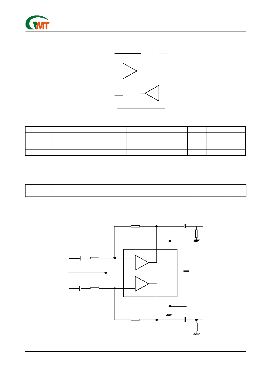
Block Diagram
Absolute Maximum Ratings
(Note1)
SYMBOL PARAMETER
CONDITIONS
MIN.
MAX.
UNIT
V
DD
Supply
voltage
0
7.0
V
T
stg
Storage
temperature
-65 +150 ∞C
T
amb
Operating ambient temperature
0
+70
∞C
ESD ESD
voltage
HBM
-
2
KV
Notes:
1. Absolute Maximum Ratings are limits beyond which damage to the device may occur.
Thermal Characteristics
SYMBOL PARAMETER VALUE
UNIT
R
th j-a
Thermal resistance from junction to ambient in free air SO8
210
∞C/W
Test and Application Information
Fig.1 Measurement circuit for inverting application
_
+
_
+
2
3
V
DD
V
INA
3.9k
3.9k
V
ref
(typ. 2.5V)
V
INB
3.9k
5
6
7
4
1
8
G1401
3.9k
+
220µF
V
OUTA
R
L
+
C6
100µF
220µF
+
R
L
V
OUTB
2.2µF
2.2µF
_
+
_
+
G1401
1
2
3
4
5
6
7
8
OUTA
INA(neg)
INA(pos)
V
SS
V
DD
OUTB
INB(neg)
INB(pos)

Ver 1.1
Aug 13, 2001
TEL: 886-3-5788833
http://www.gmt.com.tw
3
G1401
Global Mixed-mode Technology Inc.
Electrical Characteristics
V
DD
= 5V; V
SS
= 0V ; T
amb
= 25∞C; f
i
= 1kHz; R
L
= 32
; unless otherwise specified.
SYMBOL PARAMETER
CONDITIONS
MIN.
TYP.
MAX.
UNIT
Supplies
Supply
voltage
3.0 5.0 7.0 V
Single
3.0 5.0 7.0 V
V
DD
Dual
1.5 2.5 3.5 V
V
SS
Negative supply voltage
-1.5
-2.5
-3.5
V
I
DD
Supply current
no load
-
3.0
5.5
mA
P
tot
Total power dissipation
no load
-
15
28
mW
DC Characteristics
V
I(OS)
Input offset voltage
-15
-
15
mV
V
CM
Common mode voltage
0
-
4.0
V
CMRR
Common-Mode Rejection Ratio
V
CM
= 0V to 5V
40
60
dB
G
V
Open-loop voltage gain
R
L
= 5k
70 90 - dB
I
O
Maximum output current
THD<0.1%
-
100
-
mA
R
O
Output
resistance
open-loop
R
L
= 20
- 1.78 -
R
L
= 32
note 1
1.0 - 4.0 V
V
O
Output voltage swing
R
L
= 5k
note 1
0.1 - 4.9 V
PSRR
Power supply rejection ratio
fi = 1kHz;
V
ripple(peak)
= 1V
50 62 - dB
CS
Channel separation
-
70
-
dB
AC Characteristics
note 2
THD
Total harmonic distortion
R
L
= 5k
note 2
- <
0.1 - %
f
G
Unity gain frequency
open-loop; R
L
= 5k
2.5 3.7 5.0
MHz
P
O
Maximum output power
note 1; R
L
= 16
- 135 - mW
B
Power bandwidth
unity gain inverting
-
30
-
kHz
Notes:
1. Values are proportional to V
DD
; THD < 0.1%
2. V
DD
= 5.0V; V
O(P-P)
= 4.0V (at 0 dB)

Ver 1.1
Aug 13, 2001
TEL: 886-3-5788833
http://www.gmt.com.tw
4
G1401
Global Mixed-mode Technology Inc.
Output Swing Range Voltage Figure
Test Condition
T
A
= 25∞C, A
V
= -1
V+ = 2.5V , V- = - 2.5V , R
L
=5k
V+ = 1.5V , V- = - 1.5V , R
L
=5k
V+ = 2.5V , V- = - 2.5V , R
L
=2k
V+ = 1.5V , V- = - 1.5V , R
L
=2k
V+ = 2.5V , V- = - 2.5V , R
L
=32
V+ = 1.5V , V- = - 1.5V , R
L
=32
V+ = 2.5V , V- = - 2.5V , R
L
=16
V+ = 1.5V , V- = - 1.5V , R
L
=16

Ver 1.1
Aug 13, 2001
TEL: 886-3-5788833
http://www.gmt.com.tw
5
G1401
Global Mixed-mode Technology Inc.
Input Common Mode Voltage Range Figure
Test Condition
T
A
= 25∞C, A
V
= 1
V+ = 5V, V- = 0V, R
L
= 5K
V+ = 3V, V- = 0V, R
L
= 5k
Open-Loop Gain & Phase vs. Frequency
0.0
20.0
40.0
60.0
80.0
100.0
0.1
1
10
100
1000
10000
Frequency - kHZ
Gai
n
- dB
-150
-130
-110
-90
-70
-50
P
has
e-
degree
Test Condition: Vs = ±2.5V, T
A
= 25∞C
PSRR
0.0
10.0
20.0
30.0
40.0
50.0
60.0
70.0
0.1
1
10
100
1000
Frequency - kHZ
Power Supply Rejection - dB
PSRR +
PSRR -
Test Condition: Vs = ±2.5V, T
A
= 25∞C