 | –≠–ª–µ–∫—Ç—Ä–æ–Ω–Ω—ã–π –∫–æ–º–ø–æ–Ω–µ–Ω—Ç: G218AT-S4 | –°–∫–∞—á–∞—Ç—å:  PDF PDF  ZIP ZIP |
Ver 3.3
Sep 11, 2001
TEL: 886-3-5788833
http://www.gmt.com.tw
1
G218A
Global Mixed-mode Technology Inc.
Multi-mode LVD/SE SCSI Terminator
Features
Auto-selectable multi-mode Single-Ended
or LVD Termination
Meets SCSI-1, SCSI-2, SCSI-3 SPI Ultra
(Fast-20), Ultra 2(SPI-2 LVD), Ultra160 stan-
dards.
Supports active negation
Current limit and thermal protection
Hot-Swap compatible (Single-Ended)
5% tolerance on SE and LVD termination
resistance
28 and 36 pin SSOP package
28 Pin SSOP: Pin Compatible with DS2119
36 Pin SSOP: Pin Compatible with DS2118,
LX5241 and UCC5630
Applications
Server and workstation
High-end PC
Industrial PC
Disk Array (RAID)
SCSI cable
General Description
The G218A Multi-mode LVD/SE SCSI terminator pro-
vides a smooth transition into the next generation of
the SCSI Parallel Interface (SPI-2). It automatically
senses the bus, via DIFFSENS, and switches the ter-
mination to either single-ended (SE) or low voltage
differential (LVD) SCSI, dependent on which type of
devices are connected to the bus. If the G218A de-
tects a HVD SCSI device, it switches to a high imped-
ance state. For a 16-bit Wide SCSI bus to be opera-
tional, three G218A terminators are needed.
The Multi-mode terminator contains all functions re-
quired to terminate and auto detect and switch modes
for SCSI parallel Interface (SPI-2) bus architectures.
For the SE termination, one regulator and nine preci-
sion 110ohm resistors are used. For the LVD termina-
tion, the G218A integrates two regulated supplies with
nine precision resistor strings.
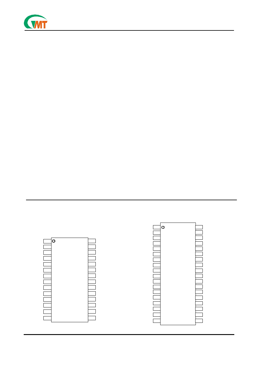
Pin Configuration
(Top View)
NC
NC
R1+
R1-
R2-
HS/GND
HS/GND
R3+
R3-
R4+
R4-
R5+
R5-
DISCNCT
GND
TPWR
HVD
LVD
SE
R9-
R9+
R8-
R8+
HS/GND
HS/GND
HS/GND
R7-
R7+
R6-
R6+
DIFFB
DIFFSENSE
M/S
VREF
R2+
HS/GND
36Pin SSOP
G218A
1
2
3
4
28
27
26
25
5
6
7
8
9
10
11
12
13
14
24
23
22
21
20
19
16
17
15
18
33
32
31
30
29
36
35
34
NC
NC
R1+
R1-
R2-
HS/GND
HS/GND
R3+
R3-
R4+
R4-
R5+
R5-
DISCNCT
GND
TPWR
HVD
LVD
SE
R9-
R9+
R8-
R8+
HS/GND
HS/GND
HS/GND
R7-
R7+
R6-
R6+
DIFFB
DIFFSENSE
M/S
VREF
R2+
HS/GND
36Pin SSOP
G218A
1
2
3
4
28
27
26
25
5
6
7
8
9
10
11
12
13
14
24
23
22
21
20
19
16
17
15
18
33
32
31
30
29
36
35
34
R1-
R1+
R2-
NC
R3+
R3-
R4+
R4-
R5+
R5-
DISCNCT
GND
TPWR
R9-
R9+
R8+
R8-
R7-
R6-
R6+
DIFFB
DIFFSENSE
M/S
28Pin SSOP/TSSOP
VREF
R2+
TPWR
R7+
G218A
1
2
3
4
28
27
26
25
5
6
7
8
9
10
11
12
13
14
24
23
22
21
20
19
18
17
16
15
NC

Ver 3.3
Sep 11, 2001
TEL: 886-3-5788833
http://www.gmt.com.tw
2
G218A
Global Mixed-mode Technology Inc.
Ordering Information
PART NUMBER
TEMP. RANGE
PIN-PACKAGE
FEATURE
G218AT-S4
0∫C-70∫C
SSOP-28 pin / Tube
DISCNCT does not disable VREF
G218AR-S4
0∫C-70∫C
SSOP-28 pin / Tape & Reel
DISCNCT does not disable VREF
G218AT-S5
0∫C-70∫C
SSOP-36 pin / Tube
DISCNCT does not disable VREF
G218AR-S5
0∫C-70∫C
SSOP-36 pin / Tape & Reel
DISCNCT does not disable VREF
G218AT-D3
0∫C-70∫C
TSSOP-28 pin / Tube
DISCNCT does not disable VREF
G218AR-D3
0∫C-70∫C
TSSOP-28 pin / Tape & Reel
DISCNCT does not disable VREF
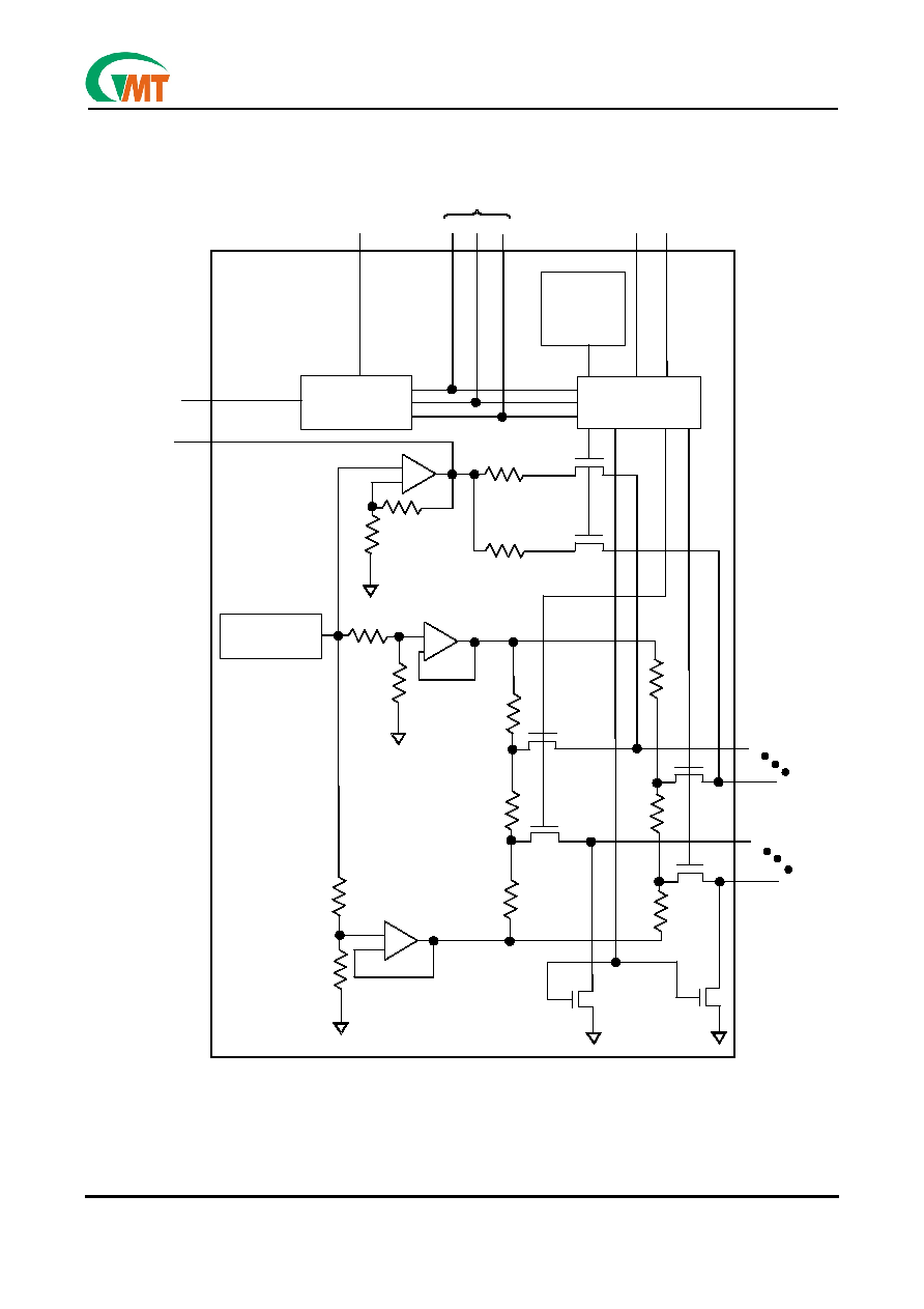
Functional Description
The G218A combines LVD and SE termination with
DIFFSENS sourcing and detection. The LVD termina-
tion section consists of two source/sink amplifiers
(VTOP, VBOT), biasing circuitry and nine precision
resistor strings (RTOP, RMID, RBOT). The SE termi-
nation section consists of a 2.85V source/sink regula-
tor with 9 precision 110ohm resistor. The DIFFSENSE
section consists of a 1.3V, 5mA driver and a sensing
circuit (Figure 1)
DIFFSENSE is used by multi-mode transceiver
(LVD/SE) to determine if the device is connected to a
single-ended, LVD or HVD SCSI bus. If the voltage on
DIFFSENSE is between 0-0.5V the bus is sin-
gle-ended; if it is between 0.7-1.9V the bus is LVD;
and if it is greater than 2.4V, the bus is HVD.
The G218A DIFFB pin monitors the DIFFSENS line to
determine the proper operating mode of the device;
this mode is indicated by the SE/LVD/HVD outputs.
The DIFFSENSE pin can also drive the SCSI
DIFFSENS line (when M/S=1) to determine the SCSI
bus operating mode. The G218A switches to the ter-
mination mode that is appropriate for the bus based on
the value of the DIFFSENS voltage. These modes are:
LVD mode LVD termination is provided by a precision
resistor string with two amplifiers. This configuration
yields a 105
differential and 150
common mode
impedance. A fail safe bias of 112mV is maintained
when no drivers are connected to the SCSI bus.
SE mode When the external driver for a given signal
line turns off, the active terminator will pull that signal
line to 2.85 volts (quiescent state). When used with an
active negation driver, the power amp can sink 22mA
per line.
while keeping the voltage reference in regulation. The
terminating resistors maintain their 110
value.
HVD Isolation Mode The G218A identifies that there
is an HVD (high voltage differential) device on the
SCSI bus and isolates the termination pins from the
bus.
When DISCNCT=1, the termination pins are isolated
from the SCSI bus, and the bus mode indicators
(SE/LVD/HVD) as well as VREF remains active. Dur-
ing thermal shutdown, the termination pins are isolated
from the SCSI bus and VREF becomes high imped-
ance. The DIFFSENSE driver is shut down during ei-
ther of these two events.
To ensure proper operation, the TPWR pin should be
connected to the SCSI bus TERMPWR line. As with all
analog circuitry, the TERMPWR and VDD lines should
be bypassed locally. A 2.2µF capacitor and a 0.01µF
high frequency capacitor is recommended between
TPWR and ground and placed as close as possible to
the G218A. The G218A should be placed as close as
possible to the SCSI connector to minimize signal and
power trace length, thereby resulting in less input ca-
pacitance and reflections which can degrade the bus
signals.
To maintain the specified regulation, a 4.7µF capacitor
is required between the VREF pin and ground of each
G218A. A high frequency cap (0.1µF ceramic recom-
mended) can also be placed on the VREF pin in ap-
plications that use fast rise/fall time drivers. A typical
SCSI bus configuration is shown in Figure2.
An internal pull down resistor assures that the G218A
will be terminating the bus if the DISCNCT pin is left
floating.
Note:
DIFFSENS
Refers to the SCSI bus signal.
DIFFSENSE
Refers to the G218A pin name and in-
ternal circuitry relating to differential sensing.
DIFFB
Refers to the G218A pin name and internal
circuitry relating to monitoring the DIFFSENS line.
Ver 3.3
Sep 11, 2001
TEL: 886-3-5788833
http://www.gmt.com.tw
3
G218A
Global Mixed-mode Technology Inc.
G218A Block Diagram
(Figure 1)
DIFFB
DIFFSENSE
SE LVD HVD
THERMAL
SHUTDOWN
CIRCUITRY
DISCNCT M/S
CONTROL
LOGIC
VREF
DIFFSENSE
CIRCUITRY
SE
LVD
HVD
BANDGAP
REFERENCE
VREF
110 Ohms
110 Ohms
R1-
R9-
VTOP
RTOP
RMID
RBOT
R1+
R1-
R9-
R9+
R1-
R9-
SE
GND
DRIVER
VBOT
R1+
R9+
36pin SSOP only
+
_
+
_
+
_
(
)
DIFFB
DIFFSENSE
SE LVD HVD
THERMAL
SHUTDOWN
CIRCUITRY
DISCNCT M/S
CONTROL
LOGIC
VREF
DIFFSENSE
CIRCUITRY
SE
LVD
HVD
BANDGAP
REFERENCE
VREF
110 Ohms
110 Ohms
R1-
R9-
VTOP
RTOP
RMID
RBOT
R1+
R1-
R9-
R9+
R1-
R9-
SE
GND
DRIVER
VBOT
R1+
R9+
36pin SSOP only
+
_
+
_
+
_
+
_
+
_
(
)

Ver 3.3
Sep 11, 2001
TEL: 886-3-5788833
http://www.gmt.com.tw
4
G218A
Global Mixed-mode Technology Inc.
SCSI Bus Configuration
(Figure 2)
G218A
G218A
G218A
G218A
TPWR
M/S
DISCNCT
DIFFSENSE
CONTROL LINES (9)
DIFFSENS
TPWR
TERMPWR
20K
VREF DIFFB
0.1µF
DIFFSENSE
DIFFB VREF
TERMPWR
TPWR
M/S
DISCNCT
DIFFB VREF
TPWR
DIFFB VREF
TPWR
DATA LINES (9)
VREF DIFFB
TPWR
VREF DIFFB
DATA LINES (9)
G218A
G218A
2.2µF
2.2µF
2.2µF
2.2µF
2.2µF
2.2µF
M/S
DISCNCT
M/S
DISCNCT
M/S
DISCNCT
M/S
DISCNCT
4.7µF
4.7µF
4.7µF
4.7µF
4.7µF
4.7µF
0.1µF
20K
G218A
G218A
G218A
G218A
TPWR
M/S
DISCNCT
DIFFSENSE
CONTROL LINES (9)
DIFFSENS
TPWR
TERMPWR
20K
VREF DIFFB
0.1µF
DIFFSENSE
DIFFB VREF
TERMPWR
TPWR
M/S
DISCNCT
DIFFB VREF
TPWR
DIFFB VREF
TPWR
DATA LINES (9)
VREF DIFFB
TPWR
VREF DIFFB
DATA LINES (9)
G218A
G218A
2.2µF
2.2µF
2.2µF
2.2µF
2.2µF
2.2µF
M/S
DISCNCT
M/S
DISCNCT
M/S
DISCNCT
M/S
DISCNCT
4.7µF
4.7µF
4.7µF
4.7µF
4.7µF
4.7µF
0.1µF
20K

Ver 3.3
Sep 11, 2001
TEL: 886-3-5788833
http://www.gmt.com.tw
5
G218A
Global Mixed-mode Technology Inc.
Pin Description
(for 28pin SSOP)
PIN SYMBOL
DESCRIPTION
1 VREF*
Reference Voltage. 2.85-volt reference; a regulator bypass, must be connected to a 4.7µF capacitor.
2-5,7-12,
18-21, 23-26
Rx+, Rx-
Signal Termination. (X=1,2,3,.....9)
Rx+: Ground line for single-ended or positive line for differential applications for the SCSI bus.
Rx-: Signal line/active line for single-ended or negative line in differential applications for the SCSI
bus.
6,22 NC
No Connect. Do not connect these pins.
13 DISCNCT
Disconnect. When pulled high, the G218 isolates its bus pins (Rx+, Rx-) from the SCSI bus.
14 GND
Ground. Terminator ground pin. Connected to ground.
15 M/S
Master/slave. Used to select which terminator is the controlling device. M/S pin high enables the
DIFFSENSE driver.
16
DIFFSENSE Output to drive the SCSI bus DIFFSENS line.
17 DIFFB
DIFFB pin should be connected to a 0.1µF capacitor to GND and 20k resistor to SCSI/Bus
DIFFSENS line. An input pin to detect the type of device (differential or single-ended) on the SCSI
bus.
27,28 TPWR
Terminator Power. Connect to the SCSI TERMPWR line and de-couple with a 2.2µF capacitor.
*The VREF keeps the level at 2.85 volt, despite the DISCNCT pin is asserted or not; even the termination mode is changed.
(36pin SSOP)
PIN SYMBOL
DESCRIPTION
1 VREF*
Reference Voltage. 2.85-volt reference; a regulator bypass, must be connected to a 4.7µF capaci-
tor.
2,3 NC
No Connect. Do not connect these pins.
4-7,11-16,
22-25,
29-32
Rx+
Rx-
Signal Termination. (X=1,2,3,.....9)
Rx+: Ground line for single-ended or positive line for differential applications for the SCSI bus.
Rx-: Signal line/active line for single-ended or negative line in differential applications for the SCSI bus.
8, 9,10,26,
27,28
HS/GND
Heat Sink Ground. Connect to large area PC board traces to increase power dissipation capabil-
ity.
17 DISCNCT
Disconnect. When pulled high, the G218 isolates its bus pins (Rx+, Rx-) from the SCSI bus.
18 GND
Ground. Terminator ground pin. Connected to ground.
19 M/S
Master/slave. Mode select for the non controlling terminator.
MSTR enables the DIFFSENSE driver.
20
DIFFSENSE Output to drive the SCSI bus DIFFSENS line.
21 DIFFB
DIFFB pin should be connected to a 0.1µF capacitor to GND and 20k resistor to SCSI/Bus
DIFFSENS line. An input pin to detect the type of device (differential or single-ended) on the SCSI
bus.
33 SE
Single ended mode indicator. It is HIGH when terminator is operating in SE mode.
34 LVD
Low Voltage Differential mode indicator. It is HIGH when terminator is operating in LVD mode.
35 HVD
High Voltage Differential mode indicator. It is HIGH when terminator is operating in HVD mode
or thermal shutdown.
36 TPWR
Terminator Power. Connect to SCSI bus TERMPWR line and decouple with 2.2µF capacitor.
*The VREF keeps the level at 2.85 volt, despite the DISCNCT pin is asserted or not; even the termination mode is changed.