 | –≠–ª–µ–∫—Ç—Ä–æ–Ω–Ω—ã–π –∫–æ–º–ø–æ–Ω–µ–Ω—Ç: G526-1 | –°–∫–∞—á–∞—Ç—å:  PDF PDF  ZIP ZIP |

Ver 1.0
Dec 26, 2000
TEL: 886-3-5788833
http://www.gmt.com.tw
1
G526
Global Mixed-mode Technology Inc.
Dual USB High-Side Power Switch
Features
Compliant to USB specifications
Low MOSFET on resistance at 5.0V 140m
max.
per channel
500mA minimum continuous load current per
channel
3.0V to 5.5V input
110µA typical on-state supply current
1µA typical off-state supply current
Output can be forced higher than input
(off-state)
1.25A maximum current limit
Thermal shutdown
2.4V typical undervoltage lockout (UVLO)
Open-drain fault flag pins
1ms turn-on (soft-start) and fast turnoff
Available with active-high or active-low
enable
Applications
USB host and self-powered hubs
Bus-powered hubs
Hot plug-in power supplies
Battery-charger circuits
Description
The G526 is a dual integrated high-side power switch
with independent enable and flag functions, optimized
for self-powered and bus-powered Universal Serial
Bus (USB) applications.
The G526 satisfies the following USB requirements:
the switch's low on-resistance meets USB voltage
drop requirements; fault current is limited to typically
750mA, well below the UL 25VA safety requirement;
and flag outputs are available to indicate fault condi-
tions to the local USB controller. Soft start eliminates
the momentary voltage drop on the upstream port that
may occur when the switch is enabled in bus-powered
applications.
Additional features include thermal shutdown to pre-
vent catastrophic switch failure from high-current loads,
under-voltage lockout (UVLO) ensuring that the device
remains off unless there is a valid input voltage pre-
sent, and an enable input that is compatible with both
3.3V and 5V logic.
The G526 is available in active-high and active-low
enable versions in 8-pin SOIC packages.
Ordering Information
PART ENABLE TEMP. RANGE PACKAGE
G526-1 Active
High
40∞C to
85∞C
8-Pin SOP
G526-2 Active
Low
40∞C to
85∞C
8-Pin SOP
Pin Configuration
GATE
CONTROL
GATE
CONTROL
G526
(ENA)1
(FLGA)2
(FLGB)3
(ENB)4
8(OUTA)
7 (IN)
5 (OUTB)
6 (GND)
G526
1
2
3
4
8
7
6
5
ENA
FLGA
FLGB
ENB
OUTA
IN
GND
OUTB
8 Pin SOP
Ver 1.0
Dec 26, 2000
TEL: 886-3-5788833
http://www.gmt.com.tw
2
G526
Global Mixed-mode Technology Inc.
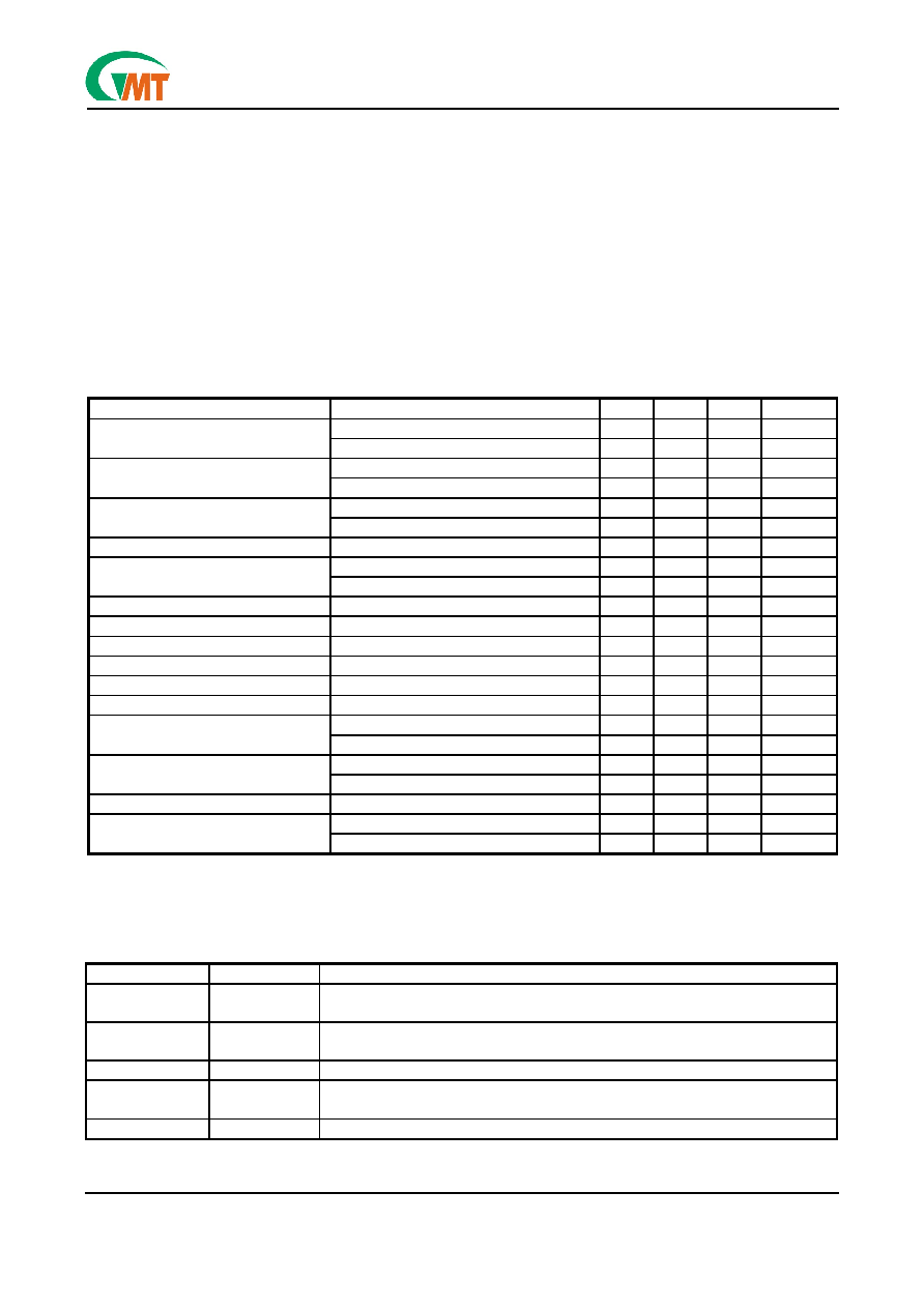
Absolute Maximum Ratings
Supply Voltage (VIN)......................................+6.0V
Fault Flag Voltage (VFLG)...............................+6.0V
Fault flag current (IFLG)..................................50mA
Output Voltage (VOUT)...................................+6.0V
Output Current (IOUT).....................Internally Limited
Control Input (VEN)................................-0.3V to 6V
Storage Temperature (TS)................-65∞C to +150∞C
Lead Temperature (Soldering 5 sec.)................260∞C
ESD protection...............................................2KV
Operating Ratings
Supply Voltage (VIN)............................+3V to +5.5V
Ambient Operating Temperature (TA)...-40∞C to +85∞C
Thermal Resistance
SOIC (
JA).........................................160∞C/W
Electrical Characteristics
(V
IN
=+5V; T
A
=25
∞
∞
∞
∞
C; unless noted.)
PARAMETER CONDITION
MIN
TYP
MAX
UNITS
Note *, switch off, OUT = open
25
µA
Supply Current
Note *, switch on, OUT = open
110
µA
low to high transition
2.4
2.5
V
Enable Input Threshold
high to low transition, Note * 1.0
2.2
V
V
EN
= VOH(min) = 2.4V
0.01
1
µA
Enable Input Current
V
EN
= VOL(max) = 0.8V
0.01
1
µA
Enable Input Capacitance
1
pF
V
IN
= 5V
100
m
Switch Resistance
V
IN
= 3V
140
m
Output Turn-On Delay
R
L
= 10
each output
1
ms
Output Turn-On Rise Time
R
L
= 10
each output
0.5
ms
Output Turn-Off Delay
R
L
= 10
each output
1
20
µs
Output Turn-Off Fall Time
R
L
= 10
each output
1
20
µs
Output Leakage Current
each output
10
µA
Short Circuit Current Limit
each output
0.5
0.75
1.25
A
T
J
increasing
135 ∞C
Overtemperature shutdown
Threshold
T
J
decreasing
125 ∞C
V
IN
= 5V, I
L
=10mA
10
Error Flag Output Resistance
V
IN
= 3.3V, I
L
=10mA
15
Error Flag Off Current
V
FLAG
= 5V
0.01
1
µA
V
IN
= increasing
2.5
V
UVLO Threshold
V
IN
= decreasing
2.3
V
General Note: Devices are ESD protected, however, handling precautions recommended.
Note *: Off is
1.0 and on is
2.4V for the G526-1. Off is
2.4V and on is
1.0V for the G526-2. The enable input
has approximately 200mV of hysteresis. See control threshold charts.
Pin Description
PIN NUMBER
PIN NAME PIN FUNCTION
1/4 EN(A/B)
Enable (input): Logic-compatible enable input. High input >2.1V typical.
Low input <1.9V typical (-1 active high, -2 active low). Do not float.
2/3 FLG(A/B)
Fault Flag (Output): Active-low, open-drain output. Indicates overcurrent, UVLO, and
thermal shutdown.
6 GND
Ground: Supply return.
7 IN
Supply Input: Output MOSFET source. Also supplies IC's internal circuitry. Connect to
positive supply.
8/5 OUT(A/B)
Switch Output: Output MOSFET drain. Typically connect to switched side of load.

Ver 1.0
Dec 26, 2000
TEL: 886-3-5788833
http://www.gmt.com.tw
3
G526
Global Mixed-mode Technology Inc.
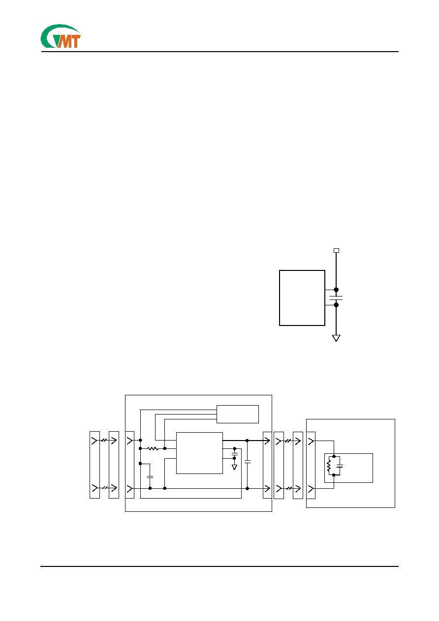
Typical Applications
Block Diagrams
Functional Description
The G526-1 and G526-2 are dual high-side switches
with active-high and active-low enable inputs, respec-
tively. Fault conditions turn off or inhibit turn-on one or
both of the output transistors, depending upon the
type of fault, and activate the open-drain error flag
transistors to pull FLG pin to ground.
Input and Output
IN (input) is the power supply connection to the logic
circuitry and the source of the output MOSFET. OUTx
(output) is the drain of the output A or B MOSFET. In a
typical circuit, current flows through the switch from IN
to OUT toward the load.
The output MOSFET and driver circuitry are also de-
signed to allow the MOSFET drain to be externally
forced to a higher voltage than the source (V
OUT
> V
IN
)
when the output is off. In this situation, the G526
avoids undesirable drain-to-body diode current flow by
connecting the body to the most positive voltage. If
V
OUT
>V
IN
when switch is enabled, current will flow
from V
OUT
to V
IN
.
Thermal Shutdown
Thermal shutdown shuts off both output MOSFETs
and signals both fault flags if the die temperature ex-
ceeds 135∞C. 10∞C of hystersis prevents the switch
from turning on until the die temperature drops to
125∞C. Overtemperature detection functions only
when at least one switch is enabled.
OUTA
OUTB
GND
ENB
ENA
CHARGE
PUMP
CHARGE
PUMP
OSC.
THERMAL
SHUTDOWN
UVLO
1.2V
REFERENCE
GATE
CONTROL
GATE
CONTROL
CURRENT
LIMIT
CURRENT
LIMIT
FLGA
IN
FLGB
G526
Upstream
V
BUS
100mA max.
V
BUS
D
+
D
GND
Data
GND
IN
OUT
3.3V USB Controller
VIN
ON/OFF
OVERCURRENT
OVERCURRENT
ON/OFF
G526
ENA OUTA
FLGA
FLGB
ENB
IN
GND
OUTB
V
CC
5.0V
47µF
0.1µF
USB
Port1
USB
Port2
Data
(Two Pair)
V
BUS
D
+
D
GND
V
BUS
D
D
+
GND
Ferrite
Beads
10k
10k
100k
100k
1µF
1µF
47µF
Ver 1.0
Dec 26, 2000
TEL: 886-3-5788833
http://www.gmt.com.tw
4
G526
Global Mixed-mode Technology Inc.
Undervoltage Lockout
UVLO (undervoltage lockout) prevents the output
MOSFET from turning on until IN (input voltage) ex-
ceeds 2.5V typical. After the switch turns on, if the
voltage drops below 2.3V typical, UVLO shuts off the
output MOSFET and signals the fault flag. Undervolt-
age detection functions only when at least one switch
is enabled.
Current Sensing and Limiting
The current limit threshold is preset internally. The
preset level prevents damage to the output MOSFET
and external load but allows a minimum current of
0.5A through the output MOSFET.
A current sense circuit senses the output current of
MOSFET switch. If output current exceeds the current
limit threshold, the output MOSFET switch is shut off
and a fault flag is pulled low. The reaction to an over-
current is measured with the following scenarios:
Switch Enable into Heavy Load
If a switch is powered-on or enabled into a heavy load
or short-circuit, the switch immediately goes into a
constant-current mode, reducing output voltage. The
fault flag goes low until the load is reduced or thermal
shutdown occurs.
Heavy Load Applied Suddenly to Enabled Switch
When a heavy load is applied, a large current may
flow from the output capacitor and the switch. The
current limit circuit may shut the switch off briefly, then
fold back into constant-current mode. In that case, the
fault flag falls until the load is reduced.
Fault Flag
FLG is an N-channel, open-drain MOSFET output.
The fault-flag is active (low) for one or more of the
following conditions: undervoltage, current limit, or
thermal shutdown. The flag output MOSFET is capa-
ble of sinking a 10mA load to typically 100mV above
ground. Both flag pins may be "wire-NORed" to a
common pullup resistor.
Applications Information
Supply filtering
A 0.1
µ
F to 1
µ
F bypass capacitor from IN to GND, lo-
cated at the G526, is strongly recommended to control
supply transients. Without a bypass capacitor, an out-
put short may cause sufficient ringing on the input
(from supply lead inductance) to damage internal con-
trol circuitry.
Input or output transients must not exceed the abso-
lute maximum supply voltage (VIN max = 6V) even for
a short duration.
Figure 1. Supply Bypassing
Figure 2. Soft Start (Single Channel)
ENA
FLGA
FLGB
ENB
OUTA
IN
GND
OUTB
G526
4.0V to 5.5V
0.1µF to 1µF
USB Host
GND
V
BUS
Cable
Bus Powered Hub
USB
Controller
C
BULK
4.7
µF
G526
Cable
Downstream USB Device
Capacitive
Load
1
2
3
4
8
7
6
5
OUTA
IN
GND
OUTB
ENA
FLGA
FLGB
ENB

Ver 1.0
Dec 26, 2000
TEL: 886-3-5788833
http://www.gmt.com.tw
5
G526
Global Mixed-mode Technology Inc.
Figure 3. Inrush Current-Limit Application
Enable Input
EN must be driven logic high or logic low, or be pulled
high or low for a clearly defined input. Floating the
input may cause unpredictable operation. EN should
not be allowed to go negative with respect to GND.
Soft Start
The G526 presents a high impedance when off, and
slowly becomes a low impedance as it turns on. This
reduces inrush current and related voltage drop that
results from charging a capacitive load, satisfying the
USB voltage drop requirements, for bus-powered ap-
plications as shown in Figure 2.
The soft start circuit shown in Figure 3 can be utilized
to meet USB transient regulation specifications with
large load capacitances (CBULK >10µF). The G526
will provide inrush current limiting for these applica-
tions.
Transient Overcurrent Filter
Figure 4. Transient Filter
The inrush current from the connection of a heavy ca-
pacitive load may cause the fault flag to fall for a short
duration while the switch is in a constant-current mode,
for charging the capacitance. In needed, a simple 1ms
RC low-pass filter in series with the fault flag circuit
will prevent erroneous overcurrent reporting (see Fig-
ure 4).
USB
Function
USB
Function
USB
Controller
V
BUS
Cable
4.7
µF
GND
USB Hub
C
BULK
C
BULK
G526
USB Peripheral
1
2
3
4
8
7
6
5
ENA
FLGA
FLGB
ENB
OUTA
IN
GND
OUTB
OVERCURRENT
USB Controller
0.1 µF
10k
10k
V
1
2
3
4
5
6
7
8
G526
ENA
FLGA
FLGB
ENB
OUTA
IN
GND
OUTB