 | –≠–ª–µ–∫—Ç—Ä–æ–Ω–Ω—ã–π –∫–æ–º–ø–æ–Ω–µ–Ω—Ç: 8170D18 | –°–∫–∞—á–∞—Ç—å:  PDF PDF  ZIP ZIP |

Rev: 1.04b 06/2001
1/32
© 2001, GSI Technology, Inc.
Specifications cited are design targets and are subject to change without notice. For latest documentation contact your GSI representative.
D
Preliminary
GS8170D18/36B-333/300/250
18Mb
1x2Lp DDR SRAM
1M x 18, 512K x 36
250 - 333 MHz
1.8 V V
DD
1.8 V and 1.5 V I/O
209-Bump BGA
Commercial Temp
Industrial Temp
Features
∑ Double Data Rate Read and Write mode
∑ JEDEC standard SigmaRAM
TM
pinout and package
∑ 1.8 V +150/≠100 mV core power supply
∑ 1.5 V or 1.8 V I/O supply
∑ Pipelined read operation.
∑ Fully coherent read and write pipelines
∑ Echo Clock outputs track data output drivers
∑ ZQ mode pin for user-selectable output drive strength
∑ 2 User programmable chip enable inputs for easy depth
expansion.
∑ IEEE 1149.1 JTAG-compatible Boundary Scan
∑ 209-bump, 14 mm x 22 mm, 1 mm bump pitch BGA package
∑ Pin compatible with future 32M, 64M, and 128M devices
SigmaRAM Family Overview
GS8170D18/36 SigmaRAMs are built in compliance with the
SigmaRAM pinout standard for synchronous SRAMs.
18,874,368-bit (18Mb) SRAMs. These are the first in a family
of wide, very low voltage CMOS I/O SRAMs designed to
operate at the speeds needed to implement economical high
performance networking systems.
GSI's
RAMs are offered in a number of configurations that
emulate other synchronous SRAMs, such as Burst RAMs,
NBT, Late Write, or Double Data Rate (DDR) SRAMs. The
logical differences between the protocols employed by these
RAMs hinge mainly on various combinations of address
bursting, output data registering and write cueing. The
RAM
TM
family standard allows a user to implement the
interface protocol best suited to the task at hand.
Functional Description
Because SigmaRAMs are synchronous devices, address, and
read/write control inputs are captured on the rising edge of the
input clock. Write cycles are internally self-timed and initiated
by the rising edge of the clock input. This feature eliminates
complex off-chip write pulse generation required by
asynchronous SRAMs and simplifies input signal timing. In
DDR mode the device captures Data In on both rising and
falling edges of clock and drives data on both clock edges as
well.
Because the DDR
RAM always transfers data in two halves,
A0 is internally set to 0 for the first half of each read or write
transfer, and automatically incremented to 1 for the falling
edge transfer. The address field of a DDR
RAM is always one
address pin less than the advertised index depth (e.g., the 1M x
18 has a 512k addressable index).
In Pipeline mode, single data rate
RAMs incorporate a rising-
edge-triggered output register. In DDR mode, rising- and
falling-edge-triggered output registers are employed. For read
cycles, a DDR SRAM's output data is staged at the input of an
edge-triggered output register during the access cycle and then
released to the output drivers at the next rising and subsequent
falling edge of clock.
GS817x18/36/72B
RAMs are implemented with GSI's high
performance CMOS technology and are packaged in a 209-
bump BGA.
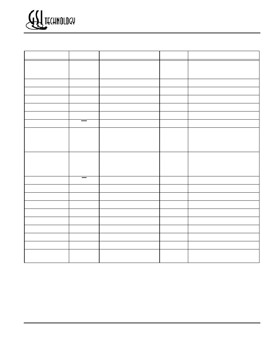
209-Bump, 14 mm x 22 mm BGA
1 mm Bump Pitch, 11 x 19 Bump Array
Bottom View

Rev: 1.04b 06/2001
2/32
© 2001, GSI Technology, Inc.
Specifications cited are design targets and are subject to change without notice. For latest documentation contact your GSI representative.
D
Preliminary
GS8170D18/36B-333/300/250
8170D36B 512K x 36 Pinout
512K x 36 Common I/O--Top View
1
2
3
4
5
6
7
8
9
10
11
A
NC
NC
A
E2
A
(16M)
ADV
A
E3
A
DQb
DQb
B
NC
NC
MCL
NC
A
W
A
MCL
NC
DQb
DQb
C
NC
NC
NC
MCL
NC
(128M)
E1
NC
NC
MCL
DQb
DQb
D
NC
NC
V
SS
NC
NC
MCL
NC
NC
V
SS
DQb
DQb
E
NC
DQPc
V
DDQ
V
DDQ
V
DD
V
DD
V
DD
V
DDQ
V
DDQ
NC
DQPb
F
DQc
DQc
V
SS
V
SS
V
SS
ZQ
V
SS
V
SS
V
SS
NC
NC
G
DQc
DQc
V
DDQ
V
DDQ
V
DD
EP2
V
DD
V
DDQ
V
DDQ
NC
NC
H
DQc
DQc
V
SS
V
SS
V
SS
EP3
V
SS
V
SS
V
SS
NC
NC
J
DQc
DQc
V
DDQ
V
DDQ
V
DD
M4
V
DD
V
DDQ
V
DDQ
NC
NC
K
CQ2
CQ2
CK
NC
V
SS
MCL
V
SS
NC
NC
CQ1
CQ1
L
NC
NC
V
DDQ
V
DDQ
V
DD
M2
V
DD
V
DDQ
V
DDQ
DQa
DQa
M
NC
NC
V
SS
V
SS
V
SS
M3
V
SS
V
SS
V
SS
DQa
DQa
N
NC
NC
V
DDQ
V
DDQ
V
DD
MCH
V
DD
V
DDQ
V
DDQ
DQa
DQa
P
NC
NC
V
SS
V
SS
V
SS
MCL
V
SS
V
SS
V
SS
DQa
DQa
R
DQPd
NC
V
DDQ
V
DDQ
V
DD
V
DD
V
DD
V
DDQ
V
DDQ
DQPa
NC
T
DQd
DQd
V
SS
NC
NC
MCL
NC
NC
V
SS
NC
NC
U
DQd
DQd
NC
A
NC (64M)
A
NC (32M)
A
NC
NC
NC
V
DQd
DQd
A
A
A
A1
A
A
A
NC
NC
W
DQd
DQd
TMS
TDI
A
MCL
A
TDO
TCK
NC
NC
∑ 2001.03
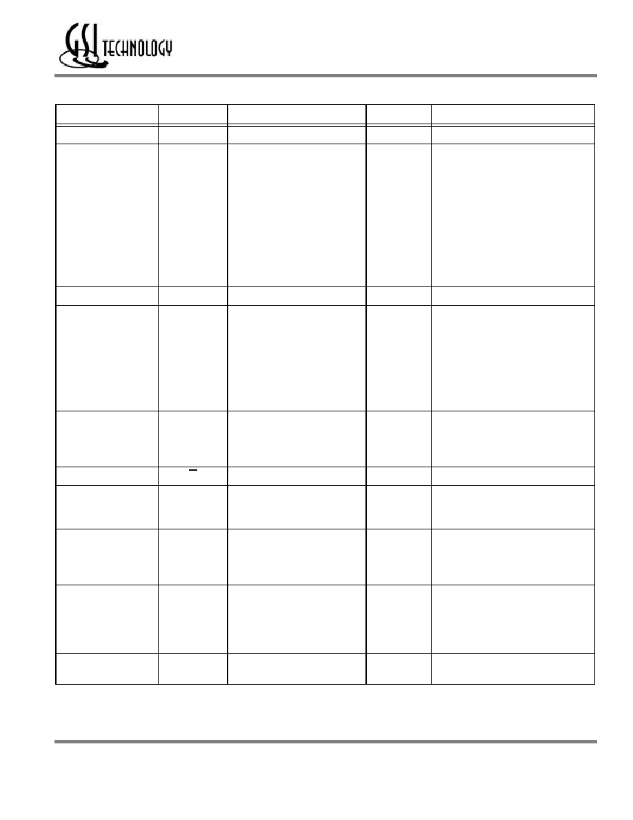
11 x 19 Bump BGA--14 x 22 mm
2
Body--1 mm Bump Pitch

Rev: 1.04b 06/2001
3/32
© 2001, GSI Technology, Inc.
Specifications cited are design targets and are subject to change without notice. For latest documentation contact your GSI representative.
D
Preliminary
GS8170D18/36B-333/300/250
8170D18 1M x 18 Pinout
1M x 18 Common I/O--Top View
1
2
3
4
5
6
7
8
9
10
11
A
NC
NC
A
E2
A
(16M)
ADV
A
E3
A
NC
NC
B
NC
NC
MCL
NC
A
W
A
NC
NC
NC
NC
C
NC
NC
NC
NC
NC
(128M)
E1
A
NC
MCL
NC
NC
D
NC
NC
V
SS
NC
NC
MCL
NC
NC
V
SS
NC
NC
E
NC
DQPb
V
DDQ
V
DDQ
V
DD
V
DD
V
DD
V
DDQ
V
DDQ
NC
NC
F
DQb
DQb
V
SS
V
SS
V
SS
ZQ
V
SS
V
SS
V
SS
NC
NC
G
DQb
DQb
V
DDQ
V
DDQ
V
DD
EP2
V
DD
V
DDQ
V
DDQ
NC
NC
H
DQb
DQb
V
SS
V
SS
V
SS
EP3
V
SS
V
SS
V
SS
NC
NC
J
DQb
DQb
V
DDQ
V
DDQ
V
DD
M4
V
DD
V
DDQ
V
DDQ
NC
NC
K
CQ2
CQ2
CK
NC
V
SS
MCL
V
SS
NC
NC
CQ1
CQ1
L
NC
NC
V
DDQ
V
DDQ
V
DD
M2
V
DD
V
DDQ
V
DDQ
DQa
DQa
M
NC
NC
V
SS
V
SS
V
SS
M3
V
SS
V
SS
V
SS
DQa
DQa
N
NC
NC
V
DDQ
V
DDQ
V
DD
MCH
V
DD
V
DDQ
V
DDQ
DQa
DQa
P
NC
NC
V
SS
V
SS
V
SS
MCL
V
SS
V
SS
V
SS
DQa
DQa
R
NC
NC
V
DDQ
V
DDQ
V
DD
V
DD
V
DD
V
DDQ
V
DDQ
DQPa
NC
T
NC
NC
V
SS
NC
NC
MCL
NC
NC
V
SS
NC
NC
U
NC
NC
NC
A
NC
(64M)
A
NC
(32M)
A
NC
NC
NC
V
NC
NC
A
A
A
A1
A
A
A
NC
NC
W
NC
NC
TMS
TDI
A
MCL
A
TDO
TCK
NC
NC
∑ 2001.03
11 x 19 Bump BGA--14 x 22 mm
2
Body--1 mm Bump Pitch
Rev: 1.04b 06/2001
4/32
© 2001, GSI Technology, Inc.
Specifications cited are design targets and are subject to change without notice. For latest documentation contact your GSI representative.
D
Preliminary
GS8170D18/36B-333/300/250
Pin Description Table
Pin Location
Symbol
Description
Type
Comments
A3, A5, A7, A9, B7, U4,
U6, U8, V3, V4, V5, V6,
V7, V8, V9, W5, W7
A
Address
Input
--
C7
A
Address
Input
x18 version only
B5
A
Address
Input
x18 and x36 versions
A6
ADV
Advance
Input
Active High
K3
CK
Clock
Input
Active High
K1, K11
CQ
Echo Clock
Output
Active High
K2, K10
CQ
Echo Clock
Output
Active Low
E2, F1, F2, G1, G2, H1,
H2, J1, J2, L10, L11,
M10, M11, N10, N11,
P10, P11, R10
DQ
Data I/O
Input/Output
x18 and x36 versions
A10, A11, B10, B11,
C10, C11, D10, D11,
E11, R1, T1, T2, U1, U2,
V1, V2, W1, W2
DQ
Data I/O
Input/Output
x36 version
C6
E1
Chip Enable
Input
Active Low
A4, A8
E2 & E3
Chip Enable
Input
Programmable Active High or Low
G6, H6
EP2 & EP3
Chip Enable Program Pin
Input
--
W9
TCK
Test Clock
Input
Active High
W4
TDI
Test Data In
Input
--
W8
TDO
Test Data Out
Output
--
W3
TMS
Test Mode Select
Input
--
L6, M6, J6
M2, M3 & M4
Mode Control Pins
Input
--
N6
MCH
Must Connect High
Input
Active High
B3, C9, D6, K6, P6, T6,
W6
MCL
Must Connect Low
Input
Active Low (all versions)
Rev: 1.04b 06/2001
5/32
© 2001, GSI Technology, Inc.
Specifications cited are design targets and are subject to change without notice. For latest documentation contact your GSI representative.
D
Preliminary
GS8170D18/36B-333/300/250
B8, C4
MCL
Must Connect Low
Input
Active Low (x36 version)
A1, A2, B1, B2, B4, B9,
C1, C2, C3, C5, C8, D1,
D2, D4, D5, D7, D8,E1,
E10, F10, F11, G10,
G11, H10, H11, J10,
J11, K4, K8, K9, L1, L2,
M1, M2, N1, N2, P1, P2,
R2, R11, T4, T5, T7, T8,
T10, T11, U3, U5, U7,
U9, U10, U11, V10, V11,
W10, W11
NC
No Connect
--
Not connected to die (all versions)
C7
NC
No Connect
--
Not connected to die (x36 version)
A1, A2, B1, B2, B4, B9,
C1, C2, C3, C8, D1, D2,
E1, E10, F10, F11, G10,
G11, H10, H11, J10,
J11, L1, L2, M1, M2, N1,
N2, P1, P2, R2, R11,
T10, T11, U10, U11,
V10, V11, W10, W11
NC
No Connect
--
Not connected to die (x36/x18 versions)
A10, A11, B8, B10, B11,
C4, C10, C11, D10, D11,
E11, R1, T1, T2, U1, U2,
V1, V2, W1, W2
NC
No Connect
--
Not connected to die (x18 version)
B6
W
Write
Input
Active Low
E5, E6, E7, G5, G7, J5,
J7, L5, L7, N5, N7, R5,
R6, R7
V
DD
Core Power Supply
Input
1.8 V Nominal
E3, E4, E8, E9, J3, J4,
J8, J9, L3, L4, L8, L9,
N3, N4, N8, N9, R3, R4,
R8, R9
V
DDQ
Output Driver Power Supply
Input
1.8 V or 1.5 V Nominal
D3, D9, F3, F4, F5, F7,
F8, F9, H3, H4, H5, H7,
H8, H9, K5, K7, M3, M4,
M5, M7, M8, M9, P3, P4,
P5, P7, P8, P9, T3, T9
V
SS
Ground
Input
--
F6
ZQ
Output Impedance Control
Input
Low = Low Impedance [High Drive]
High = High Impedance [Low Drive]
Pin Description Table
Pin Location
Symbol
Description
Type
Comments