 | –≠–ª–µ–∫—Ç—Ä–æ–Ω–Ω—ã–π –∫–æ–º–ø–æ–Ω–µ–Ω—Ç: 8180Q18 | –°–∫–∞—á–∞—Ç—å:  PDF PDF  ZIP ZIP |

Rev: 1.03e 06/2001
1/39
© 2001, GSI Technology, Inc.
Specifications cited are design targets and are subject to change without notice. For latest documentation contact your GSI representative.
D
Preliminary
GS8180Q18/36B-167/150/125
18Mb
2x2B2 HalfRate
DDR Separate I/O SRAM
125 - 167 MHz
1.8 V V
DD
1.8 V and 1.5 V I/O
209-Bump BGA
Commercial Temp
Industrial Temp
Features
∑ SigmaRAM
TM
JEDEC standard pinout and package
∑ Dual Double Data Rate interface
∑ Echo Clock outputs track data output drivers
∑ Byte Write controls sampled at data in time
∑ Slow Down mode pin (SD) extends Output Hold time
∑ 2 user-programmable chip enable inputs for easy depth
expansion
∑ HalfRate Clock Mode.
∑ Burst of 2 Read and Write
∑ 1.8 V +150/≠100 mV core power supply
∑ 1.5 V or 1.8 V HSTL Interface
∑ Pipelined read operation
∑ Fully coherent read and write pipelines
∑ ZQ mode pin for programmable output drive strength
∑ IEEE 1149.1 JTAG-compliant Boundary Scan
∑ 209-bump, 14 mm x 22 mm, 1 mm bump pitch BGA package
∑ Pin compatible with future 32M, 64M and 128M devices
SigmaRAM Family Overview
GS8180Q18/36B are built in compliance with the SigmaRAM
pinout standard for Separate I/O synchronous SRAMs. They
are 18,874,368-bit (18Mb) SRAMs. These are the first in a
family of wide, very low voltage HSTL I/O SRAMs designed
to operate at the speeds needed to implement economical high
performance networking systems.
Separate I/O SigmaRAMs are offered in a number of
configurations. Some emulate and enhance other synchronous
separate I/O SRAMs. A higher performance SDR (Single Data
Rate) Burst of 2 version is also offered. The logical differences
between the protocols employed by these RAMs hinge mainly
on various combinations of address bursting, output data
registering, and write cueing. Like the Common I/O family of
SigmaRAMs, Separate I/O
SigmaRAMs allow a user to
implement the interface protocol best suited to the task at hand.
Clocking and Addressing Schemes
A
2x2B2
SigmaRAM is a synchronous device. It employs
two input register clock inputs, K and K. K and K are
independent single ended clock inputs, not differential inputs
to a single differential clock input buffer. The device also
allows the user to manipulate the output register clock inputs
quasi independently with the C and C clock inputs. C and C are
also independent single ended clock inputs, not differential
inputs. If the C clocks are tied high, the K clocks are routed
internally to fire the output registers instead. Each
2x2B2
SigmaRAM also supplies Echo Clock outputs, CQ and CQ,
that are synchronized with read data output. When used in a
Source Synchronous clocking scheme these Echo Clock
outputs can be used to fire input registers at the data's
destination.
Because Separate I/O
2x2B2
RAMs always transfer data in
two packets, A0 is internally set to 0 for the first read or write
transfer, and automatically incremented by 1 for the next
transfer. Since the LSB is tied off internally, the address field
of a
2x2B2
RAM is always one address pin less than the
advertised index depth (e.g., the 1M x 18 has a 512K
addressable index).
-167
-150
-125
tKHKH
6.0 ns
6.6 ns
8 ns
tKHQV
1.6 ns
1.8 ns
2.1 ns
209-Bump, 14 mm x 22 mm BGA
1 mm Bump Pitch, 11 x 19 Bump Array
Bottom View
Rev: 1.03e 06/2001
2/39
© 2001, GSI Technology, Inc.
Specifications cited are design targets and are subject to change without notice. For latest documentation contact your GSI representative.
D
Preliminary
GS8180Q18/36B-167/150/125
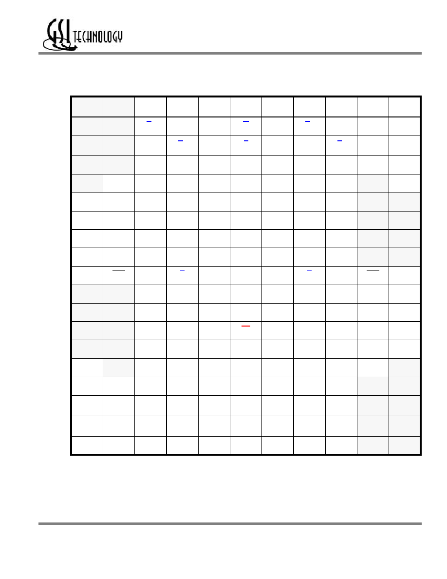
8180Q36 Pinout
512K x 36 Separate I/O--Top View
1
2
3
4
5
6
7
8
9
10
11
A
Dc1
Dc2
A
E1
A
(16M)
MCL
A
(8M)
E2
A
Qb1
Qb2
B
Dc3
Dc4
Bc
NC
A
W
A
Bb
NC
Qb3
Qb4
C
Dc5
Dc6
NC
Bd
NC
(128M)
R
NC
NC
Ba
Qb5
Qb6
D
Dc7
Dc8
V
SS
VREF
NC
MCL
NC
VREF
V
SS
Qb7
Qb8
E
Dc9
Qc1
V
DDQ
V
DDQ
V
DD
V
DD
V
DD
V
DDQ
V
DDQ
Db1
Qb9
F
Qc3
Qc2
V
SS
V
SS
V
SS
ZQ
V
SS
V
SS
V
SS
Db2
Db3
G
Qc5
Qc4
V
DDQ
V
DDQ
V
DD
EP1
V
DD
V
DDQ
V
DDQ
Db4
Db5
H
Qc7
Qc6
V
SS
V
SS
V
SS
EP2
V
SS
V
SS
V
SS
Db6
Db7
J
Qc9
Qc8
V
DDQ
V
DDQ
V
DD
M4
V
DD
V
DDQ
V
DDQ
Db8
Db9
K
CQ2
CQ2
K
K
V
SS
MCL
V
SS
C
C
CQ1
CQ1
L
Dd9
Dd8
V
DDQ
V
DDQ
V
DD
M2
V
DD
V
DDQ
V
DDQ
Qa8
Qa9
M
Dd7
Dd6
V
SS
V
SS
V
SS
M3
V
SS
V
SS
V
SS
Qa6
Qa7
N
Dd5
Dd4
V
DDQ
V
DDQ
V
DD
SD
V
DD
V
DDQ
V
DDQ
Qa4
Qa5
P
Dd3
Dd2
V
SS
V
SS
V
SS
MCL
V
SS
V
SS
V
SS
Qa2
Qa3
R
Qd9
Dd1
V
DDQ
V
DDQ
V
DD
V
DD
V
DD
V
DDQ
V
DDQ
Qa1
Da9
T
Qd7
Qd8
V
SS
VREF
NC
MCL
NC
VREF
V
SS
Da8
Da7
U
Qd5
Qd6
NC
A
NC
(64M)
A
NC
(32M)
A
NC
Da6
Da5
V
Qd3
Qd4
A
(2M)
A
A
A1
A
A
A
(4M)
Da4
Da3
W
Qd1
Qd2
TMS
TDI
A
MCL
A
TDO
TCK
Da2
Da1
Rev 11
11 x 19 Bump BGA--14 x 22 mm2 Body--1 mm Bump Pitch--MS-028vBC
Rev: 1.03e 06/2001
3/39
© 2001, GSI Technology, Inc.
Specifications cited are design targets and are subject to change without notice. For latest documentation contact your GSI representative.
D
Preliminary
GS8180Q18/36B-167/150/125
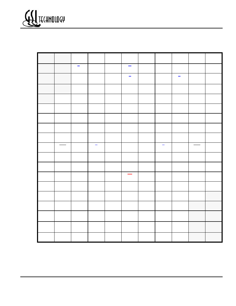
8180Q18 Pinout
1M x 18 Separate I/O--Top View
1
2
3
4
5
6
7
8
9
10
11
A
Db1
Db2
A
E1
A
(16M)
MCL
A
(8M)
E2
A
NC
NC
B
Db3
Db4
Bb
NC
A
W
A
NC
NC
NC
NC
C
Db5
Db6
NC
NC
NC
(128M)
R
A
NC
Ba
NC
NC
D
Db7
Db8
V
SS
VREF
NC
MCL
NC
VREF
V
SS
NC
NC
E
Db9
Qb1
V
DDQ
V
DDQ
V
DD
V
DD
V
DD
V
DDQ
V
DDQ
NC
NC
F
Qb3
Qb2
V
SS
V
SS
V
SS
ZQ
V
SS
V
SS
V
SS
NC
NC
G
Qb5
Qb4
V
DDQ
V
DDQ
V
DD
EP1
V
DD
V
DDQ
V
DDQ
NC
NC
H
Qb7
Qb6
V
SS
V
SS
V
SS
EP2
V
SS
V
SS
V
SS
NC
NC
J
Qb9
Qb8
V
DDQ
V
DDQ
V
DD
M4
V
DD
V
DDQ
V
DDQ
NC
NC
K
CQ2
CQ2
K
K
V
SS
MCL
V
SS
C
C
CQ1
CQ1
L
NC
NC
V
DDQ
V
DDQ
V
DD
M2
V
DD
V
DDQ
V
DDQ
Qa8
Qa9
M
NC
NC
V
SS
V
SS
V
SS
M3
V
SS
V
SS
V
SS
Qa6
Qa7
N
NC
NC
V
DDQ
V
DDQ
V
DD
SD
V
DD
V
DDQ
V
DDQ
Qa4
Qa5
P
NC
NC
V
SS
V
SS
V
SS
MCL
V
SS
V
SS
V
SS
Qa2
Qa3
R
NC
NC
V
DDQ
V
DDQ
V
DD
V
DD
V
DD
V
DDQ
V
DDQ
Qa1
Da9
T
NC
NC
V
SS
VREF
NC
MCL
NC
VREF
V
SS
Da8
Da7
U
NC
NC
NC
A
NC
(64M)
A
NC
(32M)
A
NC
Da6
Da5
V
NC
NC
A
(2M)
A
A
A1
A
A
A
(4M)
Da4
Da3
W
NC
NC
TMS
TDI
A
MCL
A
TDO
TCK
Da2
Da1
Rev 11
11 x 19 Bump BGA--14 x 22 mm2 Body--1 mm Bump Pitch--MS-028vBC

Rev: 1.03e 06/2001
4/39
© 2001, GSI Technology, Inc.
Specifications cited are design targets and are subject to change without notice. For latest documentation contact your GSI representative.
D
Preliminary
GS8180Q18/36B-167/150/125
Pin Description Table
Pin Location
Symbol
Description
Type
Comments
A3, A5, A7, A9, B5, B7, U4, U6, U8, V3,
V4, V5, V6, V7, V8, V9, W5, W7
A
Address
Input
All Versions
C7
A
Address
Input
x18 Versions
C7
NC
No Connect
--
x36 Version Only
K3
K
Clock
Input
Active High
K4
K
Clock
Input
Active Low
K9
C
Output Register Clock
Input
Active High
K8
C
Output Register Clock
Input
Active Low
K1, K11
CQ
Echo Clock
Output
Active High
K2, K10
CQ
Echo Clock
Output
Active Low
W11, W10, V11, V10, U11, U10, T11,
T10, R11
Da1 - Da9
Byte a Data Input
Input
--
E10, F10, F11, G10, G11, H10, H11,
J10, J11
Db1 - Db9
Byte b Data Input
Input
x36 Version
A1, A2, B1, B2, C1, C2, D1, D2, E1
Db1 - Db9
Byte b Data Input
Input
x18 Version
A1, A2, B1, B2, C1, C2, D1, D2, E1
Dc1 - Dc9
Byte c Data Input
Input
x36 Version
R2, P2, P1, N2, N1, M2, M1, L2, L1
Dd1 - Dd9
Byte d Data Input
Input
x36 Version
A10, A11, B10, B11, C10, C11, D10,
D11, E11
R2, P2, P1, N2, N1, M2, M1, L2, L1
E10, F10, F11, G10, G11, H10, H11,
J10, J11
W1, W2, V1, V2, U1, U2, T1, T2, R1
NC
No Connect
--
x18 Version
R10, P10, P11, N10, N11, M10, M11,
L10, L11
Qa1 - Qa9
Byte a DataOutput
Output
--
A10, A11, B10, B11, C10, C11, D10,
D11, E11
Qb1 - Qb9
Byte b DataOutput
Output
x36 Version
E2, F2, F1, G2, G1, H2, H1, J2, J1
Qb1 - Qb9
Byte b DataOutput
Output
x18 Version
E2, F2, F1, G2, G1, H2, H1, J2, J1
Qc1 - Qc9
Byte c DataOutput
Output
x36 Version
W1, W2, V1, V2, U1, U2, T1, T2, R1
Qd1 - Qd9
Byte d DataOutput
Output
x36 Version
B6
W
Write Enable
Input
Active Low
C9, B3
Ba, Bb
Byte Enable
Input
Active Low, x18 Version
B8, C4
NC
No Connect
Input
x18 Version
C9, B8
Ba, Bb
Byte Enable
Input
Active Low, x36 Version
B3, C4
Bc, Bd
Byte Enable
Input
Active Low, x36 Version
C6
R
Read Enable
Input
Active Low
A4, A8
E1 & E2
Chip Enable
Input
Programmable Active High or Low

Rev: 1.03e 06/2001
5/39
© 2001, GSI Technology, Inc.
Specifications cited are design targets and are subject to change without notice. For latest documentation contact your GSI representative.
D
Preliminary
GS8180Q18/36B-167/150/125
Note: NC = Not Connected to die or any other pin
Background
Separate I/O SigmaRAMs have been designed to be closely related to Common I/O SigmaRAMs in pinout and overall
architecture. The similarities give Separate I/O SigmaRAMs a cost advantage by allowing users and vendors to reuse supporting
infrastructure and design elements. Separate I/O SigmaRAMs come in Single and two Double Data Rate configurations. Because
they are designed to operate with both the input data pins and the output data pins operating at full speed all the time, Separate I/O
SigmaRAMs produce twice the bandwidth of Common I/O SRAMs of the same speed and output bus width. But because the
bandwidth of a memory device is set by the architecture and performance of the core array, the bandwidth available from each port
of a Separate I/O SRAM is half the bandwidth available from the single port of an otherwise equivalent Common I/O SRAM.
Separate I/O SRAMs, from a system architecture point of view, are attractive in applications where alternating reads and writes are
needed. Therefore, the SigmaRAM Separate I/O interface and truth table are optimized for alternating reads and writes. Separate I/
O SRAMs are unpopular in applications where multiple reads or multiple writes are needed because burst read or write transfers
from Separate I/O SRAMs cut the RAM's bandwidth in half.
G6, H6
EP1 & EP2
Chip Enable Program Pin
Input
--
F6
ZQ
Output Impedance Control
Input
--
W9
TCK
Test Clock
Input
Active High
W4
TDI
Test Data In
Input
--
W8
TDO
Test Data Out
Output
--
W3
TMS
Test Mode Select
Input
--
L6, M6, J6
M2, M3 & M4
Mode Control Pins
Input
--
N6
SD
Slow Down Enable
Input
Active Low
A6, D6, K6, P6, T6, W6
MCL
Must Connect Low
Input
Active Low
B4, B9, C3, C5, C8, D5, D7, T5, T7, U3,
U5, U7, U9
NC
No Connect
--
All Versions
E5, E6, E7, G5, G7, J5, J7, L5, L7, N5,
N7, R5, R6, R7
V
DD
Core Power Supply
Input
1.8 V Nominal
E3, E4, E8, E9, G3, G4, G8, G9, J3, J4,
J8, J9, L3, L4, L8, L9, N3, N4, N8, N9,
R3, R4, R8, R9
V
DDQ
Output Driver Power Supply
Input
1.8 V or 1.5 V Nominal
D4, D8, T4, T8
VREF
Input Buffer Reference Voltage
Input
--
D3, D9, F3, F4, F5, F7, F8, F9, H3, H4,
H5, H7, H8, H9, K5, K7, M3, M4, M5,
M7, M8, M9, P3, P4, P5, P7, P8, P9, T3,
T9
V
SS
Ground
Input
--
Pin Description Table
Pin Location
Symbol
Description
Type
Comments