 | –≠–ª–µ–∫—Ç—Ä–æ–Ω–Ω—ã–π –∫–æ–º–ø–æ–Ω–µ–Ω—Ç: H7546B | –°–∫–∞—á–∞—Ç—å:  PDF PDF  ZIP ZIP |

Information furnished by HAMAMATSU is believed to be reliable. However, no responsibility is assumed for possible inaccuracies or omissions. Specifications are
subject to change without notice. No patent rights are granted to any of the circuits described herein. ©2003 Hamamatsu Photonics K.K.
Subject to local technical requirements and regulations, availability of products included in this promotional material may vary. Please consult with our sales office.
MULTIANODE
PHOTOMULTIPLIER TUBE ASSEMBLY
H7546B
GENERAL
Parameter
Description / Value
Unit
Spectral Response
Wavelength of Maximum Response
Photocathode
Window Material
Dynode
Anode Size
Weight
Suitable Socket (Supplied)
Operating Ambient Temperature
Storage Temperature
nm
nm
--
mm
--
--
--
mm
g
--
∞C
∞C
300 to 650
420
Bialkali
18.1
◊ 18.1
Borosilicate glass
Metal channel dynode
12
2
◊ 2
Approx. 60
SD-108-T-22, SS-101-T-22, ASP-24307-02
-30 to +50
-30 to +50
Material
Minimum Effective Area
Structure
Number of Stages
CHARACTERISTICS (at 25
∞C)
Parameter
Unit
Cathode Sensitivity
Quantum Efficiency at 390 nm
Anode Sensitivity
Gain
Anode Dark Current per Channel (after 30 min storage in darkness)
Anode Dark Current in Total (after 30 min storage in darkness)
Time Response
(per channel)
Pulse Linearity per Channel (
±5 % deviation)
Cross-talk (with 1 mm optical fiber)
Uniformity Among All Anodes
Luminous (2856 K)
Blue Sensitivity Index (CS 5-58)
Luminous (2856 K)
Anode Pulse Rise Time
Transit Time Spread (FWHM)
80
8.5
21
24
3.0
◊ 10
5
0.2
12
1.0
0.3
0.6
2
1: 3
--
--
--
--
--
2
60
--
--
--
--
1: 5
60
6.5
--
8
--
--
--
--
--
--
--
--
µA/lm
--
%
A/lm
--
nA
nA
ns
ns
mA
%
--
Value
Min.
Tye.
Max.
NOTE: Anode characteristics are measured with the voltage distribution ratio shown below.
MAXIMUM RATINGS (Absolute Maximum Values)
Parameter
Description / Value
Unit
Supply Voltage Between Anode and Cathode
Average Anode Output Current in Total
V
µA
-1000
23
Supply Voltage: -800 V, K: Cathode, Dy: Dynode, P: Anode
VOLTAGE DISTRIBUTION RATIO AND SUPPLY VOLTAGE
Electrodes
Ratio
K
Dy3
2
Dy5
1
Dy1
3
Dy2
Dy4
2
...
1
Dy9
1 ... 1
Dy10 Dy11
1
Dy12
1
P
2
5
8 mm
◊ 8 mm Multianode, High Speed Response, Low Cross-talk
30 mm Square, Bialkali Photocathode, 12-stage, Head-on Type
MULTIANODE PHOTOMULTIPLIER TUBE ASSEMBLY H7546B
Figure 3: Typical Time Response
TPMHB0438EB
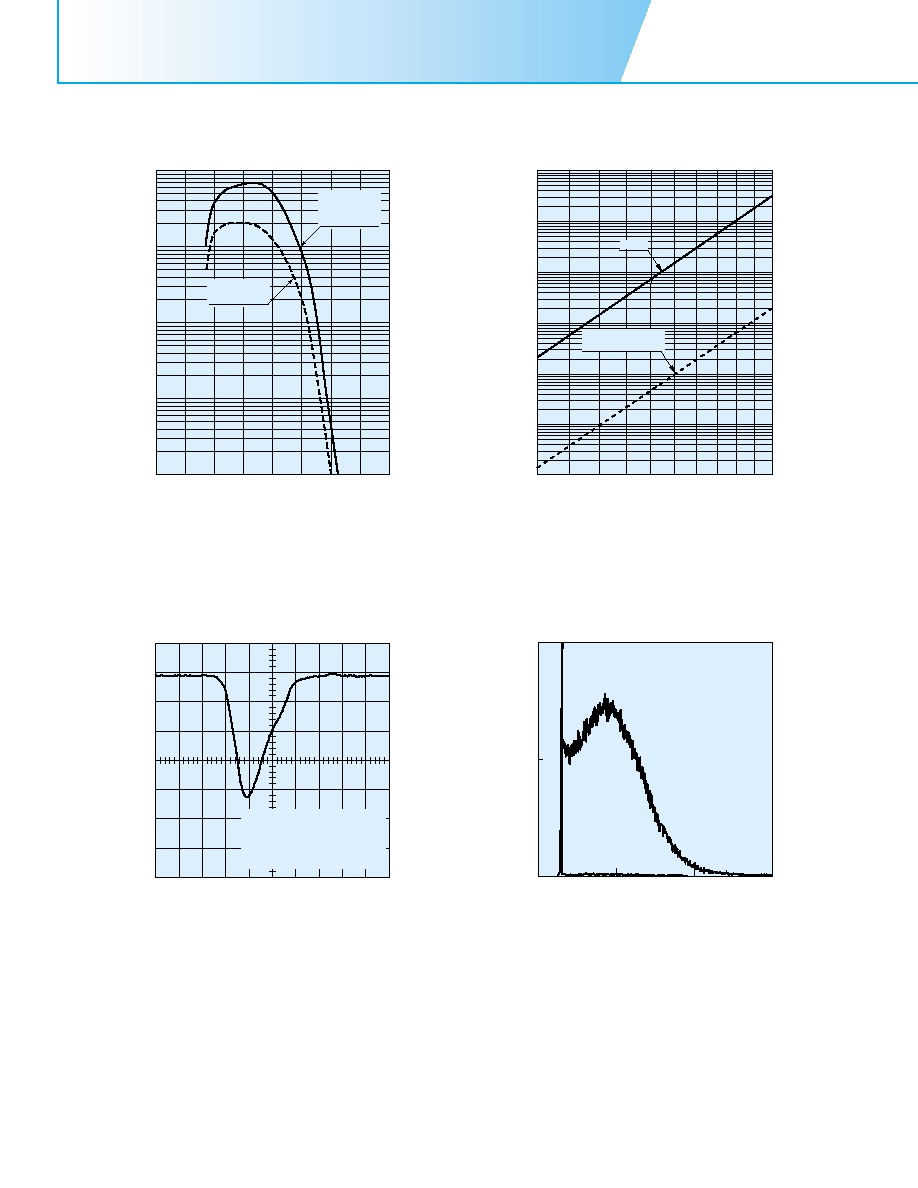
Figure 4: Single Photoelectron PHD per Channel (Example)
TPMHB0437EB
Figure 1: Typical Spectral Response
TPMHB0266EA
Figure 2: Typical Gain and Dark Current
TPMHB0439EA
500
700
SUPPLY VOLTAGE (V)
DARK CURRENT (A)
800
900
1000
600
GAIN
10
1
10
2
10
3
10
4
10
5
10
6
10
7
10
-12
10
-11
10
-10
10
-9
10
-8
10
-7
10
-6
GAIN
DARK CURRENT
per CHANNEL
WAVELENGTH (nm)
100
200
300
400
500
600
700
800
900
0.01
0.1
1
10
100
CATHODE RADIANT SENSITIVITY (mA/W)
QUANTUM EFFICIENCY (%)
QUANTUM
EFFICIENCY
CATHODE
RADIANT
SENSITIVITY
2 (ns/div.)
2 (mV/div.)
SUPPLY VOLTAGE = -800 V
RISE TIME = 1480 ps
FALL TIME = 3265 ps
WIDTH = 3120 ps
* 4 ANODES at CENTER
0
0
500
1000
0.3m
PULSE HEIGHT (ch)
DARK= =39 s
-1
COUNTS / CHANNEL
m
2m
3m
3m
0.3m
3m
0.3m
PHOTON+DARK= =5602 s
-1
m=220 [ch]
SUPPLY VOLTAGE = -900 V
WAVELENGTH = 400 nm
TEMPERATURE = 25
∞C
PHOTON COUNT = 5563 s
-1
DARK COUNT = 39 s
-1

Figure 5: Typical Anode Uniformity
TPMHB0472EB
TPMHB0587EA
Figure 6: Anode Uniformity of One Pixel
Figure 7: Anode Matrix and Guide Mark
TPMHA0404ED
Relative Anode Output
100
90
80
70
60
50
40
30
20
10
04
3.5
3
2.5
2
1.5
1
0.5
0
4
3.5
3
2.5
2
1.5
1
0.5
0
GUIDEMARK
The guide marks are holes of 0.3 mm in diameter on the electrode plate.
They can be seen from top of the H7546B through its photocathode.
They can be used for positioning when scintillating or optical fibers are
coupled to the H7546B.
Each pole corresponds to each pixel of 64 anodes.
APPLIED VOLTAGE = -800 V
LIGHT SOURCE = W LAMP (DC LIGHT)
(Full Illumination on Photocathode)
3
1
5
7
0
10
20
30
40
50
60
70
80
90
100
16
32
48
64
Number of pixel
Number of pixel
Relative Anode Output
10.21
10.46
Anode Pattern
0.3
21.4
2
0.3
1
2
3
4
5
6
7
8
57 58 59 60 61 62 63 64
4- 0.3
GUIDE MARK

TPMH1240E07
JUL. 2003 IP
HAMAMATSU PHOTONICS K.K., Electron Tube Center
314-5, Shimokanzo, Toyooka-village, Iwata-gun, Shizuoka-ken, 438-0193, Japan, Telephone: (81)539/62-5248, Fax: (81)539/62-2205
U.S.A.: Hamamatsu Corporation: 360 Foothill Road, P. O. Box 6910, Bridgewater. N.J. 08807-0910, U.S.A., Telephone: (1)908-231-0960, Fax: (1)908-231-1218 E-mail: usa@hamamatsu.com
Germany: Hamamatsu Photonics Deutschland GmbH: Arzbergerstr. 10, D-82211 Herrsching am Ammersee, Germany, Telephone: (49)8152-375-0, Fax: (49)8152-2658 E-mail: info@hamamatsu.de
France: Hamamatsu Photonics France S.A.R.L.: 8, Rue du Saule Trapu, Parc du Moulin de Massy, 91882 Massy Cedex, France, Telephone: (33)1 69 53 71 00, Fax: (33)1 69 53 71 10 E-mail: infos@hamamatsu.fr
United Kingdom: Hamamatsu Photonics UK Limited: 2 Howard Court, 10 Tewin Road Welwyn Garden City Hertfordshire AL7 1BW, United Kingdom, Telephone: 44-(0)1707-294888, Fax: 44(0)1707-325777 E-mail: info@hamamatsu.co.uk
North Europe: Hamamatsu Photonics Norden AB: Smidesv‰gen 12, SE-171-41 SOLNA, Sweden, Telephone: (46)8-509-031-00, Fax: (46)8-509-031-01 E-mail: info@hamamatsu.se
Italy: Hamamatsu Photonics Italia: S.R.L.: Strada della Moia, 1/E, 20020 Arese, (Milano), Italy, Telephone: (39)02-935 81 733, Fax: (39)02-935 81 741 E-mail: info@hamamatsu.it
WEB SITE http://www.hamamatsu.com
Figure 8: Dimensional Outline and Circuit Diagram (Unit: mm)
TPMHA0445EC
TACCA0182EA
TPMHC0179EC
NOTE: Suitable sockets for anode output pins are attached.
SOCKET for ANODE OUTPUT TERMINAL PIN
: SD-108-T-22 (Mfg. SAMTEC U.S.A.)
20.32
5.08
2.54
2.54 TYP
◊ 4pcs
0.51
1.32
2.54
0.76
3.18
7.62
1.83
PATENT US: 5410211 and other (6). GB: 551767 and other (4). DE: 69209809 and other (4). FR: 551767 and other (4).
F
K
R21
R1
R2
R3
Dy1
Dy2
Dy3
Dy4
Dy5
Dy6
Dy7
Dy8
Dy9
Dy10
Dy11
Dy12
R4
R5
R6
R7
R8
R9
R10
R11
R12
R13
R14
C1
C2
C3
C4
R15
R17
R18
R19
R20
R16
-HV INPUT
TERMINAL PIN
( 0.64)
P1
P2
P63
P64
ANODE1 OUTPUT
ANODE2 OUTPUT
ANODE63 OUTPUT
ANODE64 OUTPUT
Dy12 OUTPUT
( 0.64)
GND TERMINAL PIN
( 0.64)
.
.
.
.
.
.
R1, R5≠R14: 100 k
R2≠R4, R15: 200 k
R16: 300 k
R17≠R19: 51
R20: 10 k
R21: 1 M
C1≠C2: 0.022
µF/200 V
C3: 0.022
µF/500 V
C4: 0.01
µF/500 V
DIVIDER CURRENT: 455
µA
at 1 kV (Max. INPUT VOLTAGE)
MULTIANODE PHOTOMULTIPLIER TUBE ASSEMBLY H7546B
P1
P8
P9
P16
P17
P24
P25
(PINS CONNECTION: BOTTOM VIEW)
*A: THROUGH HOLE (NO CONNECTION)
P32
P33
P40
P41
P48
P49
P56
P57
GND
-HV
*A
GND
DY12
OUT
P64
30
±
0.5
POM CASE
DIVIDER
ASSEMBLY
SOFT TAPE
4-SCREWS (M2)
45
± 0.8
0.8 Max.
5.2
4.2
2.54
◊
7=17.78
2.54
2.54
◊9=22.86
2.54
12
3
4
5
6
7
8
57
58
59
60
61
62
63
64
25.7
0.3
2
FILLED WITH INSULATOR
TOP VIEW
SIDE VIEW
PMT:
R5900-00-M64 or
R7600-00-M64
P64
P57
P8
P1
BOTTOM VIEW
DY12 OUTPUT TERMINAL PIN ( 0.64)
; TS-101-T-A-1, SAMTEC
GND TERMINAL PIN ( 0.64)
; TS-101-T-A-1, SAMTEC
ANODE OUTPUT TERMINAL PINS
( 0.64, 2.54 PITCH, 8
◊ 8)
; TD-108-T-22, SAMTEC
◊ 4 PCS
-HV TERMINAL PINS ( 0.64)
; ASP-23882-A-1, SAMTEC