 | –≠–ª–µ–∫—Ç—Ä–æ–Ω–Ω—ã–π –∫–æ–º–ø–æ–Ω–µ–Ω—Ç: H8500 | –°–∫–∞—á–∞—Ç—å:  PDF PDF  ZIP ZIP |
52 mm Square, Bialkali Photocathode, 12-stage,
8
◊ 8 Multianode, Small Dead Space, Fast Time Response
GRing Image Cherenkov Counter
GCompact Gamma Camera
GScinti-mammography
G2D Radiation Monitor
Information furnished by HAMAMATSU is believed to be reliable. However, no responsibility is assumed for possible inaccuracies or omissions. Specifications are
subject to change without notice. No patent rights are granted to any of the circuits described herein. ©2003 Hamamatsu Photonics K.K.
Subject to local technical requirements and regulations, availability of products included in this promotional material may vary. Please consult with our sales office.
APPLICATIONS
SPECIFICATIONS
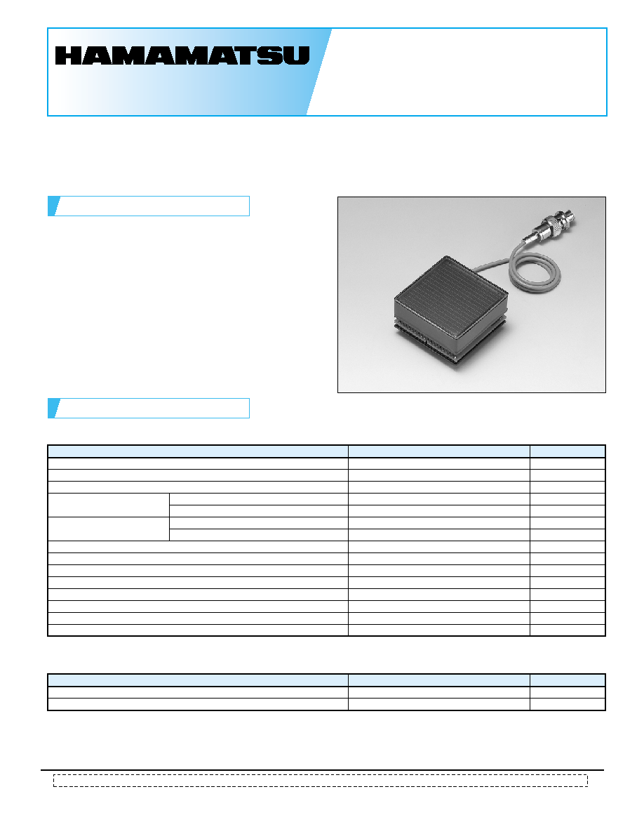
FLAT PANEL TYPE
MULTIANODE PHOTOMULTIPLIER
TUBE ASSEMBLY
H8500
TECHNICAL INFORMATION Ver. 3
J
JUN. 2003
GENERAL
Parameter
Description
Unit
Spectral Response
Peak Wavelength
Photocathode Material
Window
Dynode
Number of Anode Pixels
Pixel Size / Pitch at Center
Effective Area
Dimensional Outline (W
◊ H ◊ D)
Packing Density (Effective Area / External Size)
Weight
Operating Ambient Temperature
Storage Temperature
nm
nm
--
--
mm
--
--
--
mm
mm
mm
%
g
∞C
∞C
300 to 650
420
Bialkali
Borosilicate glass
2.0
Metal channel dynode
12
64 (8
◊ 8 matrix)
5.8
◊ 5.8 / 6.08
49
◊ 49
52
◊ 52 ◊ 28
89
145
0 to +50
-15 to +50
Material
Thickness
Structure
Number of Stage
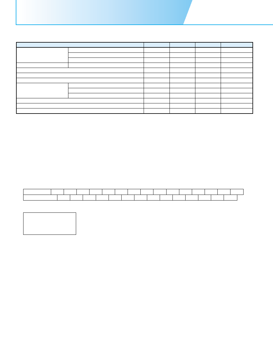
MAXIMUM RATINGS (Absolute Maximum Values)
Parameter
Value
Unit
Supply Voltage (Between Anode to Cathode)
Average Anode Output Current in Total
-1100
100
V
µA
FLAT PANEL TYPE
MULTIANODE PHOTOMULTIPLIER TUBE ASSEMBLY H8500
NOTES
A:
B:
C:
D:
E:
F:
G:
H:
The light source is a tungsten filament lamp operated at a distribution temperature of 2856 K. Supply voltage is 150 volts between the cathode and
all other electrodes connected together as anode.
The value is cathode output current when a blue filter(corning CS 5-58 polished to 1/2 stock thickness) is interposed between the light source and
the tube under the same condition as Note A.
Measured with the same light source as Note A and with the anode-to-cathode supply voltage and voltage distribution ratio shown in Table 1 below.
Measured with the same supply voltage and voltage distribution ratio as Note C after 30 minute storage in darkness.
Those are test date when a signal from a central channel of 64 anodes is used, while all photocathode are illuminated by pulsed light source.
The rise time is the time for the output pulse to rise from 10 % to 90 % of the peak amplitude when the whole photocathode is illuminated by a delta
function light pulse.
The electron transit time is the interval between the arrival of delta function light pulse at the entrance window of the tube and the time when the
anode output reaches the peak amplitude. In measurement, the whole photocathode is illuminated.
Also called transit time jitter. This is the fluctuation in electron transit time between individual pulses in the single photoelectron event, and defined
as the FWHM of the frequency distribution of electron transit time.
J:
REVISED POINTS
<From Ver.1 to Ver.2>
1) The length of assembly was changed from 31.7 mm
± 1.0 mm to 33.0 mm ± 1.0 mm.
2) The terminal connectors were changed from 32-pin type to 36-pin type.
3) The coaxial dynode output connector was removed.
4) Numbering of anode was changes from 1-1...8-8 to P1...P64.
5) The position of HV cable was moved to other side.
<From Ver.2 to Ver.3>
1) PMT length was changed from 14.7 mm
± 0.5 mm to 14.9 mm ± 0.5 mm.
2) The length of assembly was changed from 33.0 mm
± 1.0 mm to 33.2 mm ± 1.0 mm.
3) Other dimensional outline of assembly was changed accordingly.
4) The thickness of metal package was changed from 0.25 mmt to 0.5 mmt, then "
µ-METAL SHIELD" was removed.
<History of revisions>
Ver.1 issued on June 2002
Ver.2 issued on Oct. 2002
Ver.3 issued on May 2003
Please see REVISED POINTS
Table 1: Voltage Distribution Ratio and Supply Voltage
CHARACTERISTICS (at 25
∞C)
Parameter
Min.
Unit
Cathode Sensitivity
Anode Sensitivity
Gain
C
Anode Dark Current per Channel
D
Anode Dark Current in Total
D
Time Response
E
Pulse Linearity per Channel (
±2 % deviation)
Uniformity (Condition Figure 3)
Cross-talk
Luminous
A
Blue Sensitivity Index (CS 5-58)
B
Quantum Efficiency at 420 nm
Luminous
C
Rise Time
F
Transit Time
G
Transit Time Spread (FWHM)
H
40
5.5
--
--
1
◊ 10
5
--
--
--
--
--
--
--
--
55
7.5
19
55
1
◊ 10
6
0.5
32
0.8
6
0.4
1
1: 3
3
µA/lm
--
%
A/lm
--
nA
nA
ns
ns
ns
mA
--
%
--
--
--
--
--
--
100
--
--
--
--
1: 6
--
Typ.
Max.
Supply Voltage: -1000 V, K: Cathode, Dy: Dynode, GR: Guard Ring P: Anode
Electrodes
Distribution Ratio
K
Dy1
1
Dy2
1
Dy3
1
Dy4
1
Dy5
1
Dy6
1
Dy7
1
1
Dy8
Dy9
Dy10 Dy11 Dy12
GR
P
1
1
1
1
0.9
0.1
Figure 1: Typical Spectral Response
Figure 2: Typical Gain Characteristics
Figure 3: Anode Uniformity (Example)
Figure 4: Anode Matrix and Separation Mark
PHOTOCATHODE
RADIANT
SENSITIVITY
QUANTUM
EFFICIENCY
100
10
1
0.1
0.01
0.001
200
300
400
500
WAVELENGTH (nm)
PHOTOCATHODE RADIANT SENSITIVITY (mA/W)
QUANTUM EFFICIENCY (%)
600
700
800
TPMHB0695EA
TPMHB0696EB
TPMHB0697EB
TPMHB0708EA
10
7
10
6
10
5
10
4
10
3
700
800
900
1000
SUPPLY VOLTAGE (V)
GAIN
1100
P8
P1
P64
P8
56
79
83
77
65
61
66
50
58
85
83
76
60
53
59
44
58
77
79
74
59
53
47
36
54
72
73
65
43
47
50
38
53
71
72
73
59
59
62
47
50
70
83
91
86
81
72
53
53
75
91
100
95
92
83
65
44
68
78
85
84
82
78
61
SUPPLY VOLTAGE: -1000 V
LIGHT SOURCE: W-LAMP (UNIFORM DC LIGHT)
SPOT ILLUMINATION (APERTURE SIZE): 6 mm square on each channel
TOP VIEW
The start mark and the separation marks are
put on an electrode plate inside.
P1
P9
P17
P25
P33
P44
P49
P57
P2
P10
P18
P26
P34
P42
P50
P58
P3
P11
P19
P27
P35
P43
P51
P59
P4
P12
P20
P28
P36
P44
P52
P60
P5
P13
P21
P29
P37
P45
P53
P61
P6
P14
P22
P30
P38
P46
P54
P62
P7
P15
P23
P31
P39
P47
P55
P63
P8
P16
P24
P32
P40
P48
P59
P64
TOP VIEW
START MARK
SEPARATION MARK
52.0
± 0.3
PHOTOCATHODE 49.0
6.08 6.08 6.08 6.08 6.26
6.08
6.08
6.26
6.08
6.08
6.08
6.08
6.26
6.08
6.08
6.26
46.24
23.12
23.12
TPMH1282E04
JUN. 2003 IP
Printed in Japan (500)
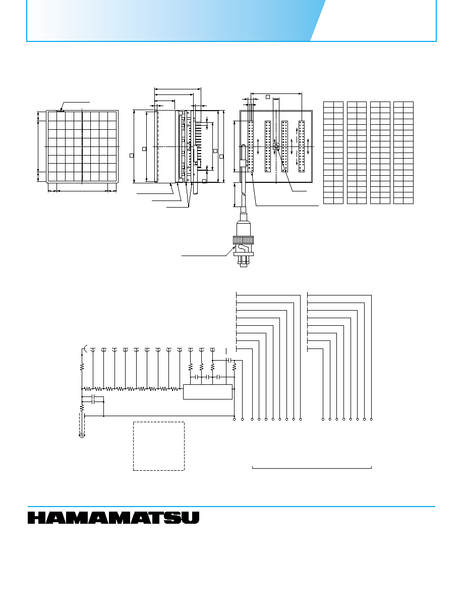
Figure 5: Dimensional Outline (Unit: mm)
HAMAMATSU PHOTONICS K.K., Electron Tube Center
314-5, Shimokanzo, Toyooka-village, Iwata-gun, Shizuoka-ken, 438-0193, Japan, Telephone: (81)539/62-5248, Fax: (81)539/62-2205
U.S.A.: Hamamatsu Corporation: 360 Foothill Road, P. O. Box 6910, Bridgewater. N.J. 08807-0910, U.S.A., Telephone: (1)908-231-0960, Fax: (1)908-231-1218 E-mail: usa@hamamatsu.com
Germany: Hamamatsu Photonics Deutschland GmbH: Arzbergerstr. 10, D-82211 Herrsching am Ammersee, Germany, Telephone: (49)8152-375-0, Fax: (49)8152-2658 E-mail: info@hamamatsu.de
France: Hamamatsu Photonics France S.A.R.L.: 8, Rue du Saule Trapu, Parc du Moulin de Massy, 91882 Massy Cedex, France, Telephone: (33)1 69 53 71 00, Fax: (33)1 69 53 71 10 E-mail: infos@hamamatsu.fr
United Kingdom: Hamamatsu Photonics UK Limited: 2 Howard Court, 10 Tewin Road Welwyn Garden City Hertfordshire AL7 1BW, United Kingdom, Telephone: 44-(0)1707-294888, Fax: 44(0)1707-325777 E-mail: info@hamamatsu.co.uk
North Europe: Hamamatsu Photonics Norden AB: Smidesv‰gen 12, SE-171-41 SOLNA, Sweden, Telephone: (46)8-509-031-00, Fax: (46)8-509-031-01 E-mail: info@hamamatsu.se
Italy: Hamamatsu Photonics Italia: S.R.L.: Strada della Moia, 1/E, 20020 Arese, (Milano), Italy, Telephone: (39)02-935 81 733, Fax: (39)02-935 81 741 E-mail: info@hamamatsu.it
WEB SITE http://www.hamamatsu.com
FLAT PANEL TYPE
MULTIANODE PHOTOMULTIPLIER TUBE ASSEMBLY H8500
TPMHA0498EC
R1 to R9
R16 to R18
R19
R20
R21
C1
C2
C3
C7
C8, C9
: 470 k
: 51
: 10 k
: 10 k
: 1 M
: 0.01
µF
: 0.022
µF
: 0.033
µF
: 0.0047
µF
: 0.015
µF
-HV
SHV-P
(COAXIAL CABLE, RED)
DY1
K
DY2
R1
R2
DY3
R3
DY4
R4
DY5
R5
DY6
R6
DY7
R7
DY8
R8
DY9
R9
R16
C1
TRANSISTOR CIRCUIT
DY12 OUTPUT
SIGNAL GND
DY10
R17
DY11
R18
DY12
GR
P1
R21
R20
C2
R19
C3
C7
C8
C9
ANODE OUTPUT (P1)
P2
ANODE OUTPUT (P2)
P3
ANODE OUTPUT (P3)
P4
ANODE OUTPUT (P4)
P5
ANODE OUTPUT (P5)
P6
ANODE OUTPUT (P6)
P7
ANODE OUTPUT (P7)
P8
ANODE OUTPUT (P8)
(P9 to P16)
(P49 to P56)
P57
ANODE OUTPUT (P57)
P58
ANODE OUTPUT (P58)
P59
ANODE OUTPUT (P59)
P60
ANODE OUTPUT (P60)
P61
ANODE OUTPUT (P61)
P62
ANODE OUTPUT (P62)
P63
ANODE OUTPUT (P63)
P64
ANODE OUTPUT (P64)
......
....
4-(DOUBLE-ROW 2 mm Pitch) CONNECTOR
GND
GND
GND
GND
GND
GND
GND
GND
GND
GND
GND
GND
GND
GND
GND
GND
GND
*
A
P7
P8
P15
P16
P23
P24
P31
P32
P39
P40
P47
P48
P55
P56
P63
P64
DY12
GND
SIG4
GND
GND
GND
GND
GND
GND
GND
GND
GND
GND
GND
GND
GND
GND
GND
GND
GND
GND
P5
P6
P13
P14
P21
P22
P29
P30
P37
P38
P45
P46
P53
P54
P61
P62
GND
*
A
SIG3
GND
GND
GND
GND
GND
GND
GND
GND
GND
GND
GND
GND
GND
GND
GND
GND
*
A
GND
P3
P4
P11
P12
P19
P20
P27
P28
P35
P36
P43
P44
P51
P52
P59
P60
GND
GND
SIG2
CONNECTION FOR SIGNAL CONNECTORS
(BOTTOM VIEW)
GND
GND
GND
GND
GND
GND
GND
GND
GND
GND
GND
GND
GND
GND
GND
GND
GND
GND
P1
P2
P9
P10
P17
P18
P25
P26
P33
P34
P41
P42
P49
P50
P57
P58
*
A
GND
SIG1
4.5
± 0.3
4
2
12
◊ 3=36
51.3
51.7
±
0.5
36
-HV
H8500
DY,
64, 63
8, 7
62
5
16, 15,
56, 55
60, 59
3
12, 11, 4,
52, 51
GND
58,
1
10, 9, 2,
57, 50, 49
14, 13, 6,
61, 54, 53
SIG4
SIG3
SIG2
SIG1
INSULATING TAPE
PLASTIC BASE
PC BOARD
4-SIGNAL OUTPUT CONNECTOR *
B
TMM-118-03-G-D, mfg. SAMTEC
NOTE *A: Polarized position of omitted pin
*B: Suitable sockets for the signal connectors will be attached.
The equivalent socket is SQT-118-01-L-D (SAMTEC).
As it doesn't have a polarized position marker,
it can be used at any positions.
-HV: SHV-P
(COAXIAL CABLE, RED)
450
±
20
PHOTOCATHODE (EFFECTIVE AREA)
49
2
2
◊
17=34
52.0
±
0.3
14.9
± 0.5
2
4
27.9
± 0.9
33.2
± 1.0
6.08
◊
6=36.48
6.26
6.26
6.08
◊ 6=36.48
6.26
6.26
P1
P9
P17
P25
P33
P41
P49
P57
P2
P10
P18
P26
P34
P42
P50
P58
P3
P11
P19
P27
P35
P43
P51
P59
P4
P12
P20
P28
P36
P44
P52
P60
P5
P13
P21
P29
P37
P45
P53
P61
P6
P14
P22
P30
P38
P46
P54
P62
P7
P15
P23
P31
P39
P47
P55
P63
P8
P16
P24
P32
P40
P48
P56
P64
TOP VIEW
SIDE VIEW
BOTTOM VIEW
0.5
M3 D: 5
START MARK